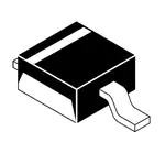
1PMT5920B Series
3.2 Watt Plastic
Surface Mount
POWERMITE® Package
This complete new line of 3.2 Watt Zener Diodes are offered in
highly efficient micro miniature, space saving surface mount with its
unique heat sink design. The POWERMITE package has the same
thermal performance as the SMA while being 50% smaller in
footprint area and delivering one of the lowest height profiles
(1.1 mm) in the industry. Because of its small size, it is ideal for use
in cellular phones, portable devices, business machines and many
other industrial/consumer applications.
Features
•
•
•
•
•
•
•
•
•
•
•
•
•
Zener Breakdown Voltage: 6.2 − 47 V
DC Power Dissipation: 3.2 W with Tab 1 (Cathode) @ 75°C
Low Leakage < 5 mA
ESD Rating of Class 3 (> 16 kV) per Human Body Model
Low Profile − Maximum Height of 1.1 mm
Integral Heat Sink/Locking Tabs
Full Metallic Bottom Eliminates Flux Entrapment
Small Footprint − Footprint Area of 8.45 mm2
Supplied in 12 mm Tape and Reel
Lead Orientation in Tape: Cathode (Short) Lead to Sprocket Holes
POWERMITE is JEDEC Registered as DO−216AA
Cathode Indicated by Polarity Band
These Devices are Pb−Free and are RoHS Compliant
Mechanical Characteristics
CASE: Void-free, transfer-molded, thermosetting plastic
FINISH: All external surfaces are corrosion resistant and leads are
readily solderable
MOUNTING POSITION: Any
MAXIMUM CASE TEMPERATURE FOR SOLDERING PURPOSES:
www.onsemi.com
PLASTIC SURFACE MOUNT
3.2 WATT ZENER DIODES
6.2 − 47 VOLTS
1
2
1: CATHODE
2: ANODE
1
2
POWERMITE
CASE 457
MARKING DIAGRAM
1
CATHODE
M
xxB
G
M
xxB G
2
ANODE
= Date Code
= Specific Device Code
(See Table on Page 2)
= Pb−Free Package
260°C for 10 Seconds
ORDERING INFORMATION
Device
Package
1PMT59xxBT1G POWERMITE
(Pb−Free)
Shipping†
3000 / Tape &
Reel
†For information on tape and reel specifications,
including part orientation and tape sizes, please
refer to our Tape and Reel Packaging Specifications
Brochure, BRD8011/D.
© Semiconductor Components Industries, LLC, 2007
December, 2018 − Rev. 5
1
Publication Order Number:
1PMT5920B/D
�1PMT5920B Series
MAXIMUM RATINGS
Rating
Symbol
Value
Unit
°PD°
RqJA
500
4.0
248
°mW
mW/°C
°C/W
RqJanode
35
°C/W
°PD°
RqJcathode
3.2
23
W
°C/W
TJ, Tstg
−55 to +150
°C
DC Power Dissipation @ TA = 25°C (Note 1)
Derate above 25°C
Thermal Resistance, Junction−to−Ambient
Thermal Resistance, Junction−to−Lead (Anode)
Maximum DC Power Dissipation (Note 2)
Thermal Resistance from Junction−to−Tab (Cathode)
Operating and Storage Temperature Range
Stresses exceeding those listed in the Maximum Ratings table may damage the device. If any of these limits are exceeded, device functionality
should not be assumed, damage may occur and reliability may be affected.
1. Mounted with recommended minimum pad size, PC board FR−4.
2. At Tab (Cathode) temperature, Ttab = 75°C
ELECTRICAL CHARACTERISTICS (TL = 25°C unless
otherwise noted, VF = 1.5 V Max. @ IF = 200 mAdc for all types)
Symbol
I
IF
Parameter
VZ
Reverse Zener Voltage @ IZT
IZT
Reverse Current
ZZT
Maximum Zener Impedance @ IZT
IZK
Reverse Current
ZZK
Maximum Zener Impedance @ IZK
IR
Reverse Leakage Current @ VR
VR
Reverse Voltage
IF
Forward Current
VF
Forward Voltage @ IF
VZ VR
V
IR VF
IZT
Zener Voltage Regulator
ELECTRICAL CHARACTERISTICS (TL = 30°C unless otherwise noted, VF = 1.25 Volts @ 200 mA)
Zener Voltage (Note 3)
VR
ZZT @ IZT
(Note 4)
ZZK @ IZK
(Note 4)
IZK
(mA)
(V)
5.0
4.0
(W)
(W)
(mA)
2.0
200
1.0
55.1
5.0
5.2
2.5
200
1.0
9.56
41.2
5.0
7.0
4.0
500
0.5
12
12.6
31.2
15
15.75
25
1.0
9.1
6.5
550
0.25
1.0
11.4
9.0
600
0.25
20.9
22
23.1
17
1.0
16.7
17.5
650
0.25
34B
22.8
24
35B
25.65
27
25.2
15.6
1.0
18.2
19
700
0.25
28.35
13.9
1.0
20.6
23
700
0.25
41B
44.65
47
49.35
8.0
1.0
35.8
67
1000
0.25
VZ @ IZT (Volts)
IZT
IR @ VR
Max
(mA)
6.51
60.5
6.8
7.14
8.64
9.1
27B
11.4
29B
14.25
1PMT5933BT1G
33B
1PMT5934BT1G
1PMT5935BT1G
1PMT5941BT1G
Device*
Device
Marking
Min
Nom
1PMT5920BT1G
20B
5.89
6.2
1PMT5921BT1G
21B
6.46
1PMT5924BT1G
24B
1PMT5927BT1G
1PMT5929BT1G
Product parametric performance is indicated in the Electrical Characteristics for the listed test conditions, unless otherwise noted. Product
performance may not be indicated by the Electrical Characteristics if operated under different conditions.
3. Zener voltage is measured with the device junction in thermal equilibrium with an ambient temperature of 25°C.
4. Zener Impedance Derivation ZZT and ZZK are measured by dividing the AC voltage drop across the device by the AC current applied. The
specified limits are for IZ(ac) = 0.1 IZ(dc) with the ac frequency = 60 Hz.
www.onsemi.com
2
�1PMT5920B Series
TYPICAL CHARACTERISTICS
100
3
IZ, ZENER CURRENT (mA)
P D , MAXIMUM POWER DISSIPATION (W)
3.5
2.5
2
TL
1.5
1
10
1
0.5
0
25
50
75
100
125
150
0.1
175
5
7
8
9
10
VZ, ZENER VOLTAGE (VOLTS)
6
T, TEMPERATURE (°C)
Figure 2. VZ to 10 Volts
10
IZ , ZENER CURRENT (mA)
100
50
30
20
10
5
3
2
1
0.5
0.3
0.2
0.1
qVZ, TEMPERATURE COEFFICIENT (mV/°C)
Figure 1. Steady State Power Derating
8
VZ @ IZT
6
4
2
0
−2
0
10
20
30
40
50
60
70
80
VZ, ZENER VOLTAGE (VOLTS)
90
100
−4
2
4
ZZ , DYNAMIC IMPEDANCE (OHMS)
qVZ, TEMPERATURE COEFFICIENT (mV/°C)
200
VZ @ IZT
100
70
50
30
20
10
6
8
10
VZ, ZENER VOLTAGE (VOLTS)
12
Figure 4. Zener Voltage − To 12 Volts
Figure 3. VZ = 12 thru 47 Volts
10
11
20
30
50
70
100
VZ, ZENER VOLTAGE (VOLTS)
200
200
IZ(dc) = 1mA
100
70
50
30
20
10
7
5
3
2
10 mA
20 mA
5
Figure 5. Zener Voltage − 14 To 47 Volts
7
iZ(rms) = 0.1 IZ(dc)
10
20
30
50
VZ, ZENER VOLTAGE (VOLTS)
Figure 6. Effect of Zener Voltage
www.onsemi.com
3
70
100
�1PMT5920B Series
Z Z , DYNAMIC IMPEDANCE (OHMS)
TYPICAL CHARACTERISTICS
1k
TJ = 25°C
iZ(rms) = 0.1 IZ(dc)
500
200
100
50
20
10
5
22 V
2
1
12 V
0.5 1
6.8 V
2
5
10
20
50 100 200
500
IZ, ZENER TEST CURRENT (mA)
Figure 7. Effect of Zener Current
C, CAPACITANCE (pF)
10,000
1000
MEASURED @ 0 V BIAS
MEASURED @ 50% VR
100
10
1
10
VZ, REVERSE ZENER VOLTAGE (VOLTS)
Figure 8. Capacitance versus Reverse
Zener Voltage
POWERMITE is a registered trademark of and used under a license from Microsemi Corporation.
www.onsemi.com
4
100
�MECHANICAL CASE OUTLINE
PACKAGE DIMENSIONS
POWERMITE
CASE 457
ISSUE G
DATE 12 JAN 2022
SCALE 4:1
GENERIC
MARKING DIAGRAMS*
1
M
XXXG
2
1
STYLE 1
1
M
XXXG
2
STYLE 2
M
XXXG
2
XXX = Specific Device Code
M = Date Code
G
= Pb−Free Package
STYLE 3
DOCUMENT NUMBER:
DESCRIPTION:
STYLE 1:
PIN 1. CATHODE
2. ANODE
98ASB14853C
POWERMITE
STYLE 2:
PIN 1. ANODE OR CATHODE
2. CATHODE OR ANODE
(BI−DIRECTIONAL)
STYLE 3:
PIN 1. ANODE
2. CATHODE
*This information is generic. Please refer to
device data sheet for actual part marking.
Pb−Free indicator, “G” or microdot “G”, may
or may not be present. Some products may
not follow the Generic Marking.
Electronic versions are uncontrolled except when accessed directly from the Document Repository.
Printed versions are uncontrolled except when stamped “CONTROLLED COPY” in red.
PAGE 1 OF 1
onsemi and
are trademarks of Semiconductor Components Industries, LLC dba onsemi or its subsidiaries in the United States and/or other countries. onsemi reserves
the right to make changes without further notice to any products herein. onsemi makes no warranty, representation or guarantee regarding the suitability of its products for any particular
purpose, nor does onsemi assume any liability arising out of the application or use of any product or circuit, and specifically disclaims any and all liability, including without limitation
special, consequential or incidental damages. onsemi does not convey any license under its patent rights nor the rights of others.
© Semiconductor Components Industries, LLC, 2019
www.onsemi.com
�onsemi,
, and other names, marks, and brands are registered and/or common law trademarks of Semiconductor Components Industries, LLC dba “onsemi” or its affiliates
and/or subsidiaries in the United States and/or other countries. onsemi owns the rights to a number of patents, trademarks, copyrights, trade secrets, and other intellectual property.
A listing of onsemi’s product/patent coverage may be accessed at www.onsemi.com/site/pdf/Patent−Marking.pdf. onsemi reserves the right to make changes at any time to any
products or information herein, without notice. The information herein is provided “as−is” and onsemi makes no warranty, representation or guarantee regarding the accuracy of the
information, product features, availability, functionality, or suitability of its products for any particular purpose, nor does onsemi assume any liability arising out of the application or use
of any product or circuit, and specifically disclaims any and all liability, including without limitation special, consequential or incidental damages. Buyer is responsible for its products
and applications using onsemi products, including compliance with all laws, regulations and safety requirements or standards, regardless of any support or applications information
provided by onsemi. “Typical” parameters which may be provided in onsemi data sheets and/or specifications can and do vary in different applications and actual performance may
vary over time. All operating parameters, including “Typicals” must be validated for each customer application by customer’s technical experts. onsemi does not convey any license
under any of its intellectual property rights nor the rights of others. onsemi products are not designed, intended, or authorized for use as a critical component in life support systems
or any FDA Class 3 medical devices or medical devices with a same or similar classification in a foreign jurisdiction or any devices intended for implantation in the human body. Should
Buyer purchase or use onsemi products for any such unintended or unauthorized application, Buyer shall indemnify and hold onsemi and its officers, employees, subsidiaries, affiliates,
and distributors harmless against all claims, costs, damages, and expenses, and reasonable attorney fees arising out of, directly or indirectly, any claim of personal injury or death
associated with such unintended or unauthorized use, even if such claim alleges that onsemi was negligent regarding the design or manufacture of the part. onsemi is an Equal
Opportunity/Affirmative Action Employer. This literature is subject to all applicable copyright laws and is not for resale in any manner.
PUBLICATION ORDERING INFORMATION
LITERATURE FULFILLMENT:
Email Requests to: orderlit@onsemi.com
onsemi Website: www.onsemi.com
◊
TECHNICAL SUPPORT
North American Technical Support:
Voice Mail: 1 800−282−9855 Toll Free USA/Canada
Phone: 011 421 33 790 2910
Europe, Middle East and Africa Technical Support:
Phone: 00421 33 790 2910
For additional information, please contact your local Sales Representative
�


 工商网监
湘ICP备2023018690号
工商网监
湘ICP备2023018690号
