DATA SHEET
www.onsemi.com
1.5 Watt Plastic
Surface Mount
Zener Voltage Regulators
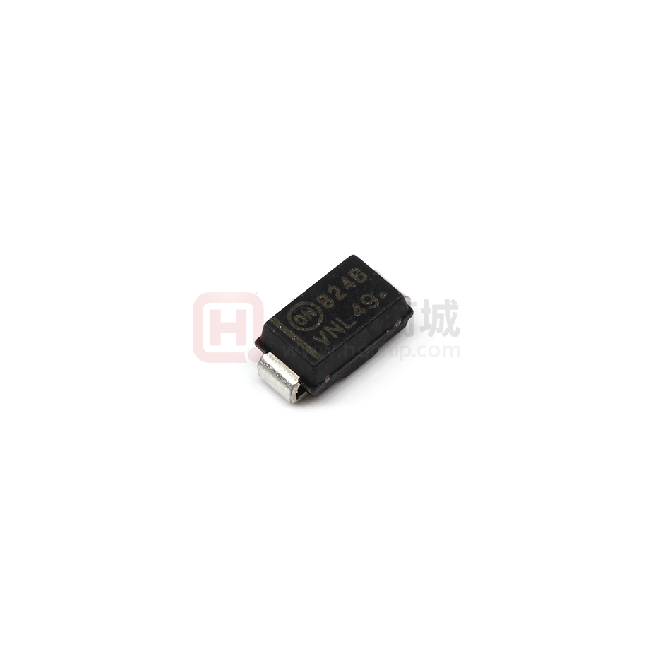
SMA
CASE 403D
STYLE 1
1SMA59xxBT3G Series,
SZ1SMA59xxBT3G Series
This complete new line of 1.5 Watt Zener Diodes offers the
following advantages.
CATHODE
Features
•
•
•
•
•
•
•
•
•
Standard Zener Breakdown Voltage Range − 3.3 V to 68 V
ESD Rating of Class 3 (> 16 kV) per Human Body Model
Flat Handling Surface for Accurate Placement
Package Design for Top Slide or Bottom Circuit Board Mounting
Low Profile Package
Ideal Replacement for MELF Packages
AEC−Q101 Qualified and PPAP Capable − SZ1SMA59xxBT3G
SZ Prefix for Automotive and Other Applications Requiring Unique
Site and Control Change Requirements
These are Pb−Free Devices*
Mechanical Characteristics:
CASE: Void-free, transfer-molded plastic
FINISH: All external surfaces are corrosion resistant with readily
solderable leads
MAXIMUM CASE TEMPERATURE FOR SOLDERING PURPOSES:
260°C for 10 seconds
POLARITY: Cathode indicated by molded polarity notch or cathode
band
FLAMMABILITY RATING: UL 94 V−0 @ 0.125 in
MAXIMUM RATINGS
Rating
DC Power Dissipation @ TL = 75°C,
Measured Zero Lead Length (Note 1)
Derate above 75°C
Thermal Resistance, Junction−to−Lead
Symbol
PD
RqJL
DC Power Dissipation @ TA = 25°C (Note 2)
Derate above 25°C
Thermal Resistance, Junction−to−Ambient
PD
RqJA
Operating and Storage Temperature Range
TJ, Tstg
Value
Unit
1.5
20
50
W
mW/°C
°C/W
0.5
4.0
250
W
mW/°C
°C/W
−65 to
+150
°C
ANODE
MARKING DIAGRAM
8xxB
AYWWG
8xxB
A
Y
WW
G
= Device Code (Refer to page 2)
= Assembly Location
= Year
= Work Week
= Pb−Free Package
ORDERING INFORMATION
Package
Shipping†
1SMA59xxBT3G
SMA
(Pb−Free)
5,000 /
Tape & Reel
SZ1SMA59xxBT3G
SMA
(Pb−Free)
5,000 /
Tape & Reel
Device
†For information on tape and reel specifications,
including part orientation and tape sizes, please
refer to our Tape and Reel Packaging Specifications
Brochure, BRD8011/D.
DEVICE MARKING INFORMATION
See specific marking information in the device marking
column of the Electrical Characteristics table on page 2 of
this data sheet.
Stresses exceeding those listed in the Maximum Ratings table may damage the
device. If any of these limits are exceeded, device functionality should not be
assumed, damage may occur and reliability may be affected.
1. 1 in square copper pad, FR−4 board.
2. FR−4 Board, using onsemi minimum recommended footprint.
*For additional information on our Pb−Free strategy and soldering details, please
download the onsemi Soldering and Mounting Techniques Reference Manual,
SOLDERRM/D.
© Semiconductor Components Industries, LLC, 2016
August, 2021 − Rev. 11
1
Publication Order Number:
1SMA5913BT3/D
�1SMA59xxBT3G Series, SZ1SMA59xxBT3G Series
ELECTRICAL CHARACTERISTICS (TA = 25°C unless
otherwise noted, VF = 1.2 V Max. @ IF = 200 mA for all types)
Symbol
I
Parameter
IF
VZ
Reverse Zener Voltage @ IZT
IZT
Reverse Current
ZZT
Maximum Zener Impedance @ IZT
IZK
Reverse Current
ZZK
Maximum Zener Impedance @ IZK
VZ VR
IR
Reverse Leakage Current @ VR
VR
Reverse Voltage
IF
Forward Current
VF
Forward Voltage @ IF
IZM
Maximum DC Zener Current
V
IR VF
IZT
Zener Voltage Regulator
ELECTRICAL CHARACTERISTICS (TA = 25°C unless otherwise noted, VF = 1.2 V Max. @ IF = 200 mA for all types)
Zener Voltage (Note 4)
Leakage Current
Device
Marking
@ IZT
ZZT @ IZT
Min
Nom
Max
mA
W
W
mA
mA
Volts
mA(dc)
1SMA5913BT3G
1SMA5914BT3G
1SMA5915BT3G
1SMA5916BT3G
813B
814B
815B
816B
3.13
3.42
3.70
4.08
3.3
3.6
3.9
4.3
3.47
3.78
4.10
4.52
113.6
104.2
96.1
87.2
10
9.0
7.5
6.0
500
500
500
500
1.0
1.0
1.0
1.0
50
35.5
12.5
2.5
1.0
1.0
1.0
1.0
455
417
385
349
1SMA5917BT3G
1SMA5918BT3G
1SMA5919BT3G
1SMA5920BT3G
817B
818B
819B
820B
4.46
4.84
5.32
5.89
4.7
5.1
5.6
6.2
4.94
5.36
5.88
6.51
79.8
73.5
66.9
60.5
5.0
4.0
2.0
2.0
500
350
250
200
1.0
1.0
1.0
1.0
2.5
2.5
2.5
2.5
1.5
2.0
3.0
4.0
319
294
268
242
1SMA5921BT3G
1SMA5922BT3G
1SMA5923BT3G
1SMA5924BT3G
821B
822B
823B
824B
6.46
7.12
7.79
8.64
6.8
7.5
8.2
9.1
7.14
7.88
8.61
9.56
55.1
50
45.7
41.2
2.5
3.0
3.5
4.0
200
400
400
500
1.0
0.5
0.5
0.5
2.5
2.5
2.5
2.5
5.2
6.0
6.5
7.0
221
200
183
165
1SMA5925BT3G
1SMA5926BT3G
1SMA5927BT3G
1SMA5928BT3G
825B
826B
827B
828B
9.5
10.45
11.4
12.35
10
11
12
13
10.5
11.55
12.6
13.65
37.5
34.1
31.2
28.8
4.5
5.5
6.5
7.0
500
550
550
550
0.25
0.25
0.25
0.25
2.5
0.5
0.5
0.5
8.0
8.4
9.1
9.9
150
136
125
115
1SMA5929BT3G
1SMA5930BT3G
1SMA5931BT3G
1SMA5932BT3G
829B
830B
831B
832B
14.25
15.2
17.1
19
15
16
18
20
15.75
16.8
18.9
21
25
23.4
20.8
18.7
9.0
10
12
14
600
600
650
650
0.25
0.25
0.25
0.25
0.5
0.5
0.5
0.5
11.4
12.2
13.7
15.2
100
94
83
75
1SMA5933BT3G
1SMA5934BT3G
1SMA5935BT3G
1SMA5936BT3G
833B
834B
835B
836B
20.9
22.8
25.65
28.5
22
24
27
30
23.1
25.2
28.35
31.5
17
15.6
13.9
12.5
17.5
19
23
26
650
700
700
750
0.25
0.25
0.25
0.25
0.5
0.5
0.5
0.5
16.7
18.2
20.6
22.8
68
63
56
50
1SMA5937BT3G
1SMA5938BT3G
1SMA5939BT3G
1SMA5940BT3G
837B
838B
839B
840B
31.35
34.2
37.05
40.85
33
36
39
43
34.65
37.8
40.95
45.15
11.4
10.4
9.6
8.7
33
38
45
53
800
850
900
950
0.25
0.25
0.25
0.25
0.5
0.5
0.5
0.5
25.1
27.4
29.7
32.7
45
42
38
35
1SMA5941BT3G
841B
44.65
47
49.35
8.0
67
1000
0.25
1SMA5942BT3G
842B
48.45
51
53.55
7.3
70
1100
0.25
1SMA5943BT3G
843B
53.2
56
58.8
6.7
86
1300
0.25
1SMA5945BT3G
845B
64.6
68
71.4
5.5
120
1700
0.25
3. Tolerance and Voltage Regulation Designation − The type number listed indicates a tolerance of ±5%.
4. VZ limits are to be guaranteed at thermal equilibrium.
* Include SZ-prefix devices where applicable.
0.5
0.5
0.5
0.5
35.8
38.8
42.6
51.7
32
29
27
22
Device* (Note 3)
VZ (Volts)
Zener Impedance
www.onsemi.com
2
ZZK @ IZK
IR @ VR
IZM
�1SMA59xxBT3G Series, SZ1SMA59xxBT3G Series
4
100
3.2
IZ, ZENER CURRENT (mA)
PD , MAXIMUM POWER DISSIPATION (WATTS)
RATING AND TYPICAL CHARACTERISTIC CURVES (TA = 25°C)
2.4
TL
1.6
10
1
0.8
TA
0
0.1
0
25
50
75
100
T, TEMPERATURE (°C)
125
150
0
2
Figure 1. Steady State Power Derating
θVZ , TEMPERATURE COEFFICIENT (mV/ °C)
IZ, ZENER CURRENT (mA)
10
1
0.1
10
20
50
60
30
40
VZ, ZENER VOLTAGE (VOLTS)
70
10
10
8
6
4
2
0
-2
-4
80
VZ @ IZT
2
4
Figure 3. VZ = 12 thru 68 Volts
6
8
VZ, ZENER VOLTAGE (VOLTS)
10
12
Figure 4. Zener Voltage − 3.3 to 12 Volts
100
70
ZZ, DYNAMIC IMPEDANCE (OHMS)
θVZ , TEMPERATURE COEFFICIENT (mV/ °C)
8
Figure 2. VZ − 3.3 thru 10 Volts
100
0
4
6
VZ, ZENER VOLTAGE (VOLTS)
VZ @ IZT
50
30
20
100
IZ(dc) = 1 mA
10
10 mA
20 mA
10
10
20
30
50
VZ, ZENER VOLTAGE (VOLTS)
70
100
IZ(rms) = 0.1 IZ(dc)
10
100
VZ, ZENER VOLTAGE (VOLTS)
Figure 6. Effect of Zener Voltage
Figure 5. Zener Voltage − 12 to 68 Volts
www.onsemi.com
3
�1SMA59xxBT3G Series, SZ1SMA59xxBT3G Series
RATING AND TYPICAL CHARACTERISTIC CURVES (TA = 25°C)
1000
10
MEASURED @
VZ/2
100
NONREPETITIVE, EXPONENTIAL
PULSE WAVEFORM, TJ = 25°C
Ppk , PEAK POWER (kW)
C, CAPACITANCE (pF)
MEASURED @
ZERO BIAS
1
0.1
TJ = 25°C
10
0.01
10
BREAKDOWN VOLTAGE (VOLTS)
100
0.01
Figure 7. Capacitance Curve
10
Figure 8. Typical Pulse Rating Curve
120
120
TA = 25°C
PW (ID) IS DEFINED AS THE
POINT WHERE THE PEAK CURRENT
DECAYS TO 50% OF Ipp.
100
PEAK VALUE
Ippm
80
60
0.9 IPEAK
HALF VALUE - Ipp/2
40
10/1000 ms WAVEFORM
AS DEFINED BY R.E.A.
20
8/20 ms WAVEFORM
AS DEFINED BY ANSI C62.1
AND IEC 801-5.
100
CURRENT (%)
≤ 10 ms
Ippm, PEAK PULSE
Ippm, PEAK PULSE CURRENT (%)
0.1
1
TP, PULSE WIDTH (ms)
80
60
0.5 IPEAK
40
20
td
T = 8 ms
0.1 IPEAK
0
0
1
2
3
t, TIME (ms)
4
0
5
0
0.02
T
20 ms
Figure 9. Pulse Waveform
www.onsemi.com
4
0.04
0.06
t, TIME (ms)
0.08
Figure 10. Pulse Waveform
0.1
�MECHANICAL CASE OUTLINE
PACKAGE DIMENSIONS
STYLE 1
SMA
CASE 403D
ISSUE J
STYLE 2
SCALE 1:1
STYLE 1:
PIN 1. CATHODE (POLARITY BAND)
2. ANODE
DATE 22 OCT 2021
STYLE 2:
NO POLARITY
GENERIC
MARKING DIAGRAM*
xxxx
AYWWG
STYLE 1
xxxx
A
Y
WW
G
xxxx
AYWWG
STYLE 2
= Specific Device Code
= Assembly Location
= Year
= Work Week
= Pb−Free Package
*This information is generic. Please refer to
device data sheet for actual part marking.
Pb−Free indicator, “G” or microdot “G”, may
or may not be present. Some products may
not follow the Generic Marking.
DOCUMENT NUMBER:
DESCRIPTION:
98AON04079D
SMA
Electronic versions are uncontrolled except when accessed directly from the Document Repository.
Printed versions are uncontrolled except when stamped “CONTROLLED COPY” in red.
PAGE 1 OF 1
onsemi and
are trademarks of Semiconductor Components Industries, LLC dba onsemi or its subsidiaries in the United States and/or other countries. onsemi reserves
the right to make changes without further notice to any products herein. onsemi makes no warranty, representation or guarantee regarding the suitability of its products for any particular
purpose, nor does onsemi assume any liability arising out of the application or use of any product or circuit, and specifically disclaims any and all liability, including without limitation
special, consequential or incidental damages. onsemi does not convey any license under its patent rights nor the rights of others.
© Semiconductor Components Industries, LLC, 2019
www.onsemi.com
�onsemi,
, and other names, marks, and brands are registered and/or common law trademarks of Semiconductor Components Industries, LLC dba “onsemi” or its affiliates
and/or subsidiaries in the United States and/or other countries. onsemi owns the rights to a number of patents, trademarks, copyrights, trade secrets, and other intellectual property.
A listing of onsemi’s product/patent coverage may be accessed at www.onsemi.com/site/pdf/Patent−Marking.pdf. onsemi reserves the right to make changes at any time to any
products or information herein, without notice. The information herein is provided “as−is” and onsemi makes no warranty, representation or guarantee regarding the accuracy of the
information, product features, availability, functionality, or suitability of its products for any particular purpose, nor does onsemi assume any liability arising out of the application or use
of any product or circuit, and specifically disclaims any and all liability, including without limitation special, consequential or incidental damages. Buyer is responsible for its products
and applications using onsemi products, including compliance with all laws, regulations and safety requirements or standards, regardless of any support or applications information
provided by onsemi. “Typical” parameters which may be provided in onsemi data sheets and/or specifications can and do vary in different applications and actual performance may
vary over time. All operating parameters, including “Typicals” must be validated for each customer application by customer’s technical experts. onsemi does not convey any license
under any of its intellectual property rights nor the rights of others. onsemi products are not designed, intended, or authorized for use as a critical component in life support systems
or any FDA Class 3 medical devices or medical devices with a same or similar classification in a foreign jurisdiction or any devices intended for implantation in the human body. Should
Buyer purchase or use onsemi products for any such unintended or unauthorized application, Buyer shall indemnify and hold onsemi and its officers, employees, subsidiaries, affiliates,
and distributors harmless against all claims, costs, damages, and expenses, and reasonable attorney fees arising out of, directly or indirectly, any claim of personal injury or death
associated with such unintended or unauthorized use, even if such claim alleges that onsemi was negligent regarding the design or manufacture of the part. onsemi is an Equal
Opportunity/Affirmative Action Employer. This literature is subject to all applicable copyright laws and is not for resale in any manner.
PUBLICATION ORDERING INFORMATION
LITERATURE FULFILLMENT:
Email Requests to: orderlit@onsemi.com
onsemi Website: www.onsemi.com
◊
TECHNICAL SUPPORT
North American Technical Support:
Voice Mail: 1 800−282−9855 Toll Free USA/Canada
Phone: 011 421 33 790 2910
Europe, Middle East and Africa Technical Support:
Phone: 00421 33 790 2910
For additional information, please contact your local Sales Representative
�


 工商网监
湘ICP备2023018690号
工商网监
湘ICP备2023018690号
