1SMB5913BT3 Series
Preferred Device
3 Watt Plastic Surface Mount Zener Voltage Regulators
This complete new line of 3 Watt Zener diodes offers the following advantages.
Features http://onsemi.com
• • • • •
Zener Voltage Range − 3.3 V to 200 V ESD Rating of Class 3 (>16 kV) per Human Body Model Flat Handling Surface for Accurate Placement Package Design for Top Side or Bottom Circuit Board Mounting Pb−Free Packages are Available
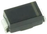
PLASTIC SURFACE MOUNT ZENER VOLTAGE REGULATOR DIODES 3.3−200 V, 3 W DC POWER
Mechanical Characteristics: CASE: Void-free, transfer-molded plastic FINISH: All external surfaces are corrosion resistant and leads are
Cathode
Anode
readily solderable
MAXIMUM LEAD TEMPERATURE FOR SOLDERING PURPOSES:
260°C for 10 Seconds
LEADS: Modified L−Bend providing more contact area to bond pads POLARITY: Cathode indicated by polarity band FLAMMABILITY RATING: UL 94 V−0 MAXIMUM RATINGS
Rating Maximum Steady State Power Dissipation @ TL = 75°C Measured at Zero Lead Length Derate Above 75°C Thermal Resistance from Junction−to−Lead Maximum Steady State Power Dissipation @ TA = 25°C (Note ) Derate Above 25°C Thermal Resistance from Junction−to−Ambient Operating and Storage Temperature Range Symbol PD Value 3.0 40 25 550 4.4 226 −65 to +150 Unit W mW/°C °C/W mW mW/°C °C/W °C
SMB CASE 403A PLASTIC
MARKING DIAGRAM
AYWW 9xxB G G A = Assembly Location Y = Year WW = Work Week 9xxB = Device Code (Refer to page 3) G = Pb−Free Package (Note: Microdot may be in either location)
RqJL PD
RqJA TJ, Tstg
ORDERING INFORMATION
Device 1SMB59xxBT3 1SMB59xxBT3G Package SMB SMB (Pb−Free) Shipping † 2500/Tape & Reel 2500/Tape & Reel
Stresses exceeding Maximum Ratings may damage the device. Maximum Ratings are stress ratings only. Functional operation above the Recommended Operating Conditions is not implied. Extended exposure to stresses above the Recommended Operating Conditions may affect device reliability. 1. FR−4 board, using recommended footprint.
†For information on tape and reel specifications, including part orientation and tape sizes, please refer to our Tape and Reel Packaging Specifications Brochure, BRD8011/D.
DEVICE MARKING INFORMATION
See specific marking information in the device marking column of the Electrical Characteristics table on page 3 of this data sheet. Preferred devices are recommended choices for future use and best overall value.
© Semiconductor Components Industries, LLC, 2006
1
July, 2006 − Rev. 6
Publication Order Number: 1SMB5913BT3/D
�1SMB5913BT3 Series
ELECTRICAL CHARACTERISTICS
(TL = 30°C unless otherwise noted, VF = 1.5 V Max. @ IF = 200 mA(dc) for all types) Symbol VZ IZT ZZT IZK ZZK IR VR IF VF IZM Parameter Reverse Zener Voltage @ IZT Reverse Current Maximum Zener Impedance @ IZT Reverse Current Maximum Zener Impedance @ IZK Reverse Leakage Current @ VR Reverse Voltage Forward Current Forward Voltage @ IF Maximum DC Zener Current VZ VR IR VF IZT V IF I
Zener Voltage Regulator
http://onsemi.com
2
�1SMB5913BT3 Series
ELECTRICAL CHARACTERISTICS (Devices listed in bold, italic are ON Semiconductor Preferred devices.)
(TL = 30°C unless otherwise noted, VF = 1.5 V Max. @ IF = 200 mA(dc) for all types) Zener Voltage (Note 3) Device* (Note 2) 1SMB5913BT3, G 1SMB5914BT3, G 1SMB5915BT3, G 1SMB5916BT3, G 1SMB5917BT3, 1SMB5918BT3, 1SMB5919BT3, 1SMB5920BT3, G G G G Device Marking 913B 914B 915B 916B 917B 918B 919B 920B 921B 922B 923B 924B 925B 926B 927B 928B 929B 930B 931B 932B 933B 934B 935B 936B 937B 938B 939B 940B 941B 942B 943B 944B 945B 946B 947B 948B 949B 950B 951B 952B 953B 954B 955B 956B VZ (Volts) Min 3.13 3.42 3.70 4.08 4.46 4.84 5.32 5.89 6.46 7.12 7.79 8.64 9.5 10.45 11.4 12.35 14.25 15.2 17.1 19 20.9 22.8 25.65 28.5 31.35 34.2 37.05 40.85 44.65 48.45 53.2 58.9 64.6 71.25 77.9 86.45 95 104.5 114 123.5 142.5 152 171 190 Nom 3.3 3.6 3.9 4.3 4.7 5.1 5.6 6.2 6.8 7.5 8.2 9.1 10 11 12 13 15 16 18 20 22 24 27 30 33 36 39 43 47 51 56 62 68 75 82 91 100 110 120 130 150 160 180 200 Max 3.47 3.78 4.10 4.52 4.94 5.36 5.88 6.51 7.14 7.88 8.61 9.56 10.5 11.55 12.6 13.65 15.75 16.8 18.9 21 23.1 25.2 28.35 31.5 34.65 37.8 40.95 45.15 49.35 53.55 58.8 65.1 71.4 78.75 86.1 95.55 105 115.5 126 136.5 157.5 168 189 210 @ IZT mA 113.6 104.2 96.1 87.2 79.8 73.5 66.9 60.5 55.1 50 45.7 41.2 37.5 34.1 31.2 28.8 25 23.4 20.8 18.7 17 15.6 13.9 12.5 11.4 10.4 9.6 8.7 8 7.3 6.7 6 5.5 5 4.6 4.1 3.7 3.4 3.1 2.9 2.5 2.3 2.1 1.9 Zener Impedance (Note 4) ZZT @ IZT W 10 9 7.5 6 5 4 2 2 2.5 3 3.5 4 4.5 5.5 6.5 7 9 10 12 14 17.5 19 23 28 33 38 45 53 67 70 86 100 120 140 160 200 250 300 380 450 600 700 900 1200 ZZK @ IZK W 500 500 500 500 500 350 250 200 200 400 400 500 500 550 550 550 600 600 650 650 650 700 700 750 800 850 900 950 1000 1100 1300 1500 1700 2000 2500 3000 3100 4000 4500 5000 6000 6500 7000 8000 mA 1 1 1 1 1 1 1 1 1 0.5 0.5 0.5 0.25 0.25 0.25 0.25 0.25 0.25 0.25 0.25 0.25 0.25 0.25 0.25 0.25 0.25 0.25 0.25 0.25 0.25 0.25 0.25 0.25 0.25 0.25 0.25 0.25 0.25 0.25 0.25 0.25 0.25 0.25 0.25 mA 100 75 25 5 5 5 5 5 5 5 5 5 5 1 1 1 1 1 1 1 1 1 1 1 1 1 1 1 1 1 1 1 1 1 1 1 1 1 1 1 1 1 1 1 Leakage Current IR @ VR Volts 1 1 1 1 1.5 2 3 4 5.2 6 6.5 7 8 8.4 9.1 9.9 11.4 12.2 13.7 15.2 16.7 18.2 20.6 22.8 25.1 27.4 29.7 32.7 35.8 38.8 42.6 47.1 51.7 56 62.2 69.2 76 83.6 91.2 98.8 114 121.6 136.8 152 IZM mA(dc) 454 416 384 348 319 294 267 241 220 200 182 164 150 136 125 115 100 93 83 75 68 62 55 50 45 41 38 34 31 29 26 24 22 20 18 16 15 13 12 11 10 9 8 7
1SMB5921BT3, G 1SMB5922BT3, G 1SMB5923BT3, G 1SMB5924BT3, G 1SMB5925BT3, G 1SMB5926BT3, G 1SMB5927BT3, G 1SMB5928BT3, G 1SMB5929BT3, G 1SMB5930BT3, G 1SMB5931BT3, G 1SMB5932BT3, G 1SMB5933BT3, G 1SMB5934BT3, G 1SMB5935BT3, G 1SMB5936BT3, G 1SMB5937BT3, G 1SMB5938BT3, G 1SMB5939BT3, G 1SMB5940BT3, G 1SMB5941BT3, 1SMB5942BT3, 1SMB5943BT3, 1SMB5944BT3, 1SMB5945BT3, 1SMB5946BT3, 1SMB5947BT3, 1SMB5948BT3, G G G G G G G G
1SMB5949BT3, G 1SMB5950BT3, G 1SMB5951BT3, G 1SMB5952BT3, G 1SMB5953BT3, 1SMB5954BT3, 1SMB5955BT3, 1SMB5956BT3, G G G G
2. TOLERANCE AND TYPE NUMBER DESIGNATION The type numbers listed indicate a tolerance of ±5%. 3. ZENER VOLTAGE (VZ) MEASUREMENT Nominal Zener voltage is measured with the device junction in thermal equilibrium with ambient temperature at 25°C. 4. ZENER IMPEDANCE (ZZ) DERIVATION ZZT and ZZK are measured by dividing the ac voltage drop across the device by the ac current applied. The specified limits are for IZ(ac) = 0.1 IZ(dc) with the ac frequency = 60 Hz. * The “G” suffix indicates Pb−Free package available.
http://onsemi.com
3
�1SMB5913BT3 Series
P D , MAXIMUM POWER DISSIPATION (WATTS) 6 PPK , PEAK SURGE POWER (WATTS) 5 4 3 2 1 TA 0 0 25 50 75 100 T, TEMPERATURE (°C) 125 150 TL 1K 500 300 200 100 50 30 20 10 0.1 0.2 0.3 0.5 1 23 5 10 20 30 50 PW, PULSE WIDTH (ms) 100 RECTANGULAR NONREPETITIVE WAVEFORM TJ = 25°C PRIOR TO INITIAL PULSE
Figure 1. Steady State Power Derating
Figure 2. Maximum Surge Power
θVZ , TEMPERATURE COEFFICIENT (mV/° C)
8 6 4 2 0 −2 −4 2
VZ @ IZT
θVZ , TEMPERATURE COEFFICIENT (mV/° C)
10
200 VZ @ IZT
100 70 50 30 20
4
6 8 VZ, ZENER VOLTAGE (VOLTS)
10
12
10 10
20
30 50 70 100 VZ, ZENER VOLTAGE (VOLTS)
200
Figure 3. Zener Voltage − To 12 Volts
Figure 4. Zener Voltage − 14 To 200 Volts
100 IZT, REVERSE CURRENT (mA) IZT, REVERSE CURRENT (mA) 50 30 20 10 5 3 2 1 0.5 0.3 0.2 0.1 0 1 2 3 4 5 6 7 VZ, ZENER VOLTAGE (VOLTS) 8 9 10
100 50 30 20 10 5 3 2 1 0.5 0.3 0.2 0.1 0 10 20 30 40 50 60 70 80 VZ, ZENER VOLTAGE (VOLTS) 90 100
Figure 5. VZ = 3.3 thru 10 Volts
Figure 6. VZ = 12 thru 82 Volts
http://onsemi.com
4
�1SMB5913BT3 Series
200 IZ(dc) = 1mA Z Z , DYNAMIC IMPEDANCE (OHMS) Z Z , DYNAMIC IMPEDANCE (OHMS) 100 70 50 30 20 10 7 5 3 2 10mA 1k 500 200 100 50 20 10 5 2 1 0.5 1 2 5 10 20 50 100 IZ, ZENER TEST CURRENT (mA) 22V 12V 200 6.8V 500 VZ =150V 91V 62V TJ = 25°C iZ(rms) = 0.1 IZ(dc)
20mA 5 7 10
iZ(rms) = 0.1 IZ(dc) 20 30 50 VZ, ZENER VOLTAGE (VOLTS) 70 100
Figure 7. Effect of Zener Voltage
Figure 8. Effect of Zener Current
Rating and Typical Characteristic Curves (TA = 25°C)
1000 MEASURED @ ZERO BIAS MEASURED @ VZ/2 10 NONREPETITIVE, EXPONENTIAL PULSE WAVEFORM, TJ = 25°C 1
100
Ppk , PEAK POWER (kW) 100
C, CAPACITANCE (pF)
0.1
TJ = 25°C 10 10 BREAKDOWN VOLTAGE (VOLTS) 0.01 0.01 0.1 1 TP, PULSE WIDTH (ms) 10
Figure 9. Capacitance Curve
Figure 10. Typical Pulse Rating Curve
120 Ippm, PEAK PULSE CURRENT (%) ≤ 10 ms PEAK VALUE Ippm 100 80 60 40 20 0
Ippm, PEAK PULSE
TA = 25°C PW (ID) IS DEFINED AS THE POINT WHERE THE PEAK CURRENT DECAYS TO 50% OF Ipp.
120 100 0.9 IPEAK CURRENT (%) 80 60 40 20 0.1 IPEAK T = 8 ms 0 0 T 20 ms 0.02 0.04 0.06 t, TIME (ms) 0.08 0.1 8/20 ms WAVEFORM AS DEFINED BY ANSI C62.1 AND IEC 801−5.
HALF VALUE − Ipp/2 10/1000 ms WAVEFORM AS DEFINED BY R.E.A. td 0 1 2 3 t, TIME (ms) 4 5
0.5 IPEAK
Figure 11. Pulse Waveform
Figure 12. Pulse Waveform
http://onsemi.com
5
�1SMB5913BT3 Series
PACKAGE DIMENSIONS
SMB CASE 403A−03 ISSUE E
HE E
NOTES: 1. DIMENSIONING AND TOLERANCING PER ANSI Y14.5M, 1982. 2. CONTROLLING DIMENSION: INCH. 3. D DIMENSION SHALL BE MEASURED WITHIN DIMENSION P. DIM A A1 b c D E HE L L1 MIN 1.90 0.05 1.96 0.15 3.30 4.06 5.21 0.76 MILLIMETERS NOM MAX 2.13 2.41 0.10 0.15 2.03 2.11 0.23 0.30 3.56 3.81 4.32 4.57 5.44 5.59 1.02 1.27 0.51 REF MIN 0.075 0.002 0.077 0.006 0.130 0.160 0.205 0.030 INCHES NOM 0.084 0.004 0.080 0.009 0.140 0.170 0.214 0.040 0.020 REF MAX 0.095 0.006 0.083 0.012 0.150 0.180 0.220 0.050
b
D
A
L
L1
c
A1
SOLDERING FOOTPRINT*
2.261 0.089
2.743 0.108
2.159 0.085
SCALE 8:1 mm inches
*For additional information on our Pb−Free strategy and soldering details, please download the ON Semiconductor Soldering and Mounting Techniques Reference Manual, SOLDERRM/D.
ON Semiconductor and are registered trademarks of Semiconductor Components Industries, LLC (SCILLC). SCILLC reserves the right to make changes without further notice to any products herein. SCILLC makes no warranty, representation or guarantee regarding the suitability of its products for any particular purpose, nor does SCILLC assume any liability arising out of the application or use of any product or circuit, and specifically disclaims any and all liability, including without limitation special, consequential or incidental damages. “Typical” parameters which may be provided in SCILLC data sheets and/or specifications can and do vary in different applications and actual performance may vary over time. All operating parameters, including “Typicals” must be validated for each customer application by customer’s technical experts. SCILLC does not convey any license under its patent rights nor the rights of others. SCILLC products are not designed, intended, or authorized for use as components in systems intended for surgical implant into the body, or other applications intended to support or sustain life, or for any other application in which the failure of the SCILLC product could create a situation where personal injury or death may occur. Should Buyer purchase or use SCILLC products for any such unintended or unauthorized application, Buyer shall indemnify and hold SCILLC and its officers, employees, subsidiaries, affiliates, and distributors harmless against all claims, costs, damages, and expenses, and reasonable attorney fees arising out of, directly or indirectly, any claim of personal injury or death associated with such unintended or unauthorized use, even if such claim alleges that SCILLC was negligent regarding the design or manufacture of the part. SCILLC is an Equal Opportunity/Affirmative Action Employer. This literature is subject to all applicable copyright laws and is not for resale in any manner.
PUBLICATION ORDERING INFORMATION
LITERATURE FULFILLMENT: Literature Distribution Center for ON Semiconductor P.O. Box 5163, Denver, Colorado 80217 USA Phone: 303−675−2175 or 800−344−3860 Toll Free USA/Canada Fax: 303−675−2176 or 800−344−3867 Toll Free USA/Canada Email: orderlit@onsemi.com N. American Technical Support: 800−282−9855 Toll Free USA/Canada Europe, Middle East and Africa Technical Support: Phone: 421 33 790 2910 Japan Customer Focus Center Phone: 81−3−5773−3850 ON Semiconductor Website: www.onsemi.com Order Literature: http://www.onsemi.com/orderlit For additional information, please contact your local Sales Representative
http://onsemi.com
6
1SMB5913BT3/D
�


 工商网监
湘ICP备2023018690号
工商网监
湘ICP备2023018690号
