2N5302 High−Power NPN Silicon Transistor
High−power NPN silicon transistors are for use in power amplifier and switching circuits applications.
Features http://onsemi.com
• Low Collector−Emitter Saturation Voltage − •
VCE(sat) = 0.75 Vdc (Max) @ IC = 10 Adc Pb−Free Package is Available*
MAXIMUM RATINGS (Note 1) (TJ = 25°C unless otherwise noted)
Rating Symbol VCEO VCB IC IB Value 60 60 30 Collector−Emitter Voltage Collector−Base Voltage
Unit Vdc Vdc Adc Adc
30 AMPERES POWER TRANSISTOR NPN SILICON 60 VOLTS, 200 WATTS
PD, POWER DISSIPATION (WATTS)
ÎÎ Î Î Î ÎÎÎÎÎÎÎÎÎÎÎÎÎÎÎÎÎÎÎ ÎÎÎÎÎÎÎÎÎÎÎÎÎÎÎÎÎÎÎ ÎÎÎ ÎÎÎ ÎÎÎ ÎÎÎÎÎÎÎÎÎÎÎÎÎÎÎÎÎÎÎ ÎÎÎÎÎÎÎÎÎÎÎÎÎÎÎÎÎÎÎ ÎÎÎÎÎÎÎÎÎÎÎÎÎÎÎÎÎÎÎ ÎÎÎÎÎÎÎÎÎÎÎÎÎÎÎÎÎÎÎ ÎÎÎ Î Î Î ÎÎÎ ÎÎÎÎÎÎÎÎÎÎÎÎÎÎÎÎÎÎÎ ÎÎÎÎÎÎÎÎÎÎÎÎÎÎÎÎÎ ÎÎÎÎÎÎÎÎÎÎÎÎÎÎÎÎÎÎÎ ÎÎÎ ÎÎÎÎÎÎÎÎÎÎÎÎÎÎÎÎÎÎÎ ÎÎÎ ÎÎÎÎÎÎÎÎÎÎÎÎÎÎÎÎÎÎÎ ÎÎ Î Î ÎÎÎ Î Î ÎÎÎÎÎÎÎÎÎÎÎÎÎÎÎÎÎÎÎ ÎÎ ÎÎÎ ÎÎÎÎÎÎÎÎÎÎÎÎÎÎÎÎÎÎÎ ÎÎÎÎÎÎÎÎÎÎÎÎÎÎÎÎÎÎÎ ÎÎÎÎÎÎÎÎÎÎÎÎÎÎÎÎÎÎÎ ÎÎÎ ÎÎÎ ÎÎÎ ÎÎÎÎÎÎÎÎÎÎÎÎÎÎÎÎÎÎÎ ÎÎÎ ÎÎÎÎ Î ÎÎÎÎÎÎÎÎÎÎÎÎÎÎÎÎÎÎÎ ÎÎÎ ÎÎÎ ÎÎ ÎÎÎÎÎÎÎÎÎÎÎÎÎÎÎÎÎÎÎ ÎÎÎÎÎÎÎÎÎÎÎÎÎÎÎÎÎÎÎ ÎÎÎÎÎÎÎÎÎÎÎÎÎÎÎÎÎÎÎ ÎÎÎÎÎÎÎÎÎÎÎÎÎÎÎÎÎ ÎÎÎÎÎÎÎÎÎÎÎÎÎÎ Î ÎÎÎÎÎÎÎÎÎÎÎÎÎÎÎÎÎÎÎ ÎÎÎÎÎÎÎÎÎÎÎÎÎÎÎÎÎÎÎ
Collector Current − Continuous (Note 2) Base Current Total Device Dissipation @ TC = 25_C Derate above 25_C Operating and Storage Junction Temperature Range 7.5 PD 200 1.14 W W/_C _C TJ, Tstg – 65 to + 200
THERMAL CHARACTERISTICS
Characteristic
Symbol qJC qCA
Max
Unit
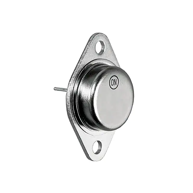
TO−204AA (TO−3) CASE 1−07 STYLE 1
Thermal Resistance, Junction−to−Case Thermal Resistance, Case−to−Ambient
0.875 34
_C/W _C/W
Stresses exceeding Maximum Ratings may damage the device. Maximum Ratings are stress ratings only. Functional operation above the Recommended Operating Conditions is not implied. Extended exposure to stresses above the Recommended Operating Conditions may affect device reliability. 1. Indicates JEDEC Registered Data. 2. Pulse Test: Pulse Width = 5 ms, Duty Cycle ≤ 10%. TA TC 8.0 200 6.0 150
MARKING DIAGRAM
2N5302G AYYWW MEX TC
4.0 100
TA
2.0
50
2N5302 G A YY WW MEX 160 180 200
= Device Code = Pb−Free Package = Location Code = Year = Work Week = Country of Origin
0
0
0
20
40
60
80 100 120 140 TEMPERATURE (°C)
ORDERING INFORMATION
Device 2N5302 Package TO−204 TO−204 (Pb−Free) Shipping 100 Units/Tray 100 Units/Tray
Figure 1. Power Temperature Derating Curve
*For additional information on our Pb−Free strategy and soldering details, please download the ON Semiconductor Soldering and Mounting Techniques Reference Manual, SOLDERRM/D.
© Semiconductor Components Industries, LLC, 2006
2N5302G
1
March, 2006− Rev. 2
Publication Order Number: 2N5302/D
�ÎÎÎ Î Î Î Î Î Î ÎÎÎÎÎÎÎÎÎÎÎÎÎÎÎÎÎÎÎÎÎÎÎÎÎÎÎÎÎÎÎÎÎ Î ÎÎ Î Î Î ÎÎÎÎÎÎÎÎÎÎÎ ÎÎ Î Î ÎÎÎÎÎÎÎ ÎÎÎÎÎÎÎÎÎÎÎÎÎÎÎÎÎÎÎÎÎÎÎÎÎÎÎÎÎÎÎÎÎ ÎÎÎ Î Î ÎÎ Î Î ÎÎÎÎÎÎÎÎÎÎÎÎÎÎÎÎÎÎÎÎÎÎÎÎÎÎÎÎÎÎÎÎÎ ÎÎÎÎÎÎÎÎÎ Î ÎÎÎÎÎÎÎ ÎÎÎÎÎÎÎÎÎÎÎÎÎÎÎÎÎÎÎÎÎÎÎÎÎÎÎÎÎÎÎÎÎ ÎÎÎÎÎÎÎÎÎÎÎÎÎÎÎÎÎÎÎÎÎÎÎÎÎÎÎÎÎÎÎÎÎ ÎÎ ÎÎ ÎÎÎÎÎÎÎÎÎÎÎÎÎÎÎÎÎÎÎÎÎÎÎÎÎÎÎÎÎÎÎÎÎ ÎÎÎÎÎÎÎÎÎÎÎÎÎÎÎÎÎÎÎÎÎÎÎÎÎÎÎÎÎÎÎÎÎ ÎÎ Î Î ÎÎÎÎ Î Î Î Î ÎÎÎÎÎÎÎÎÎÎÎÎÎÎÎÎÎÎÎÎÎÎÎÎÎÎÎÎÎÎÎÎÎ ÎÎÎÎÎÎÎÎÎÎÎÎÎÎÎÎÎÎÎÎÎÎÎÎÎÎÎÎÎÎÎÎÎ ÎÎ Î Î ÎÎÎÎÎÎÎÎÎÎÎÎÎÎÎÎÎÎÎÎÎÎÎÎÎÎÎÎÎÎÎÎÎ ÎÎÎÎÎÎÎÎÎÎÎÎÎÎÎÎÎÎÎÎÎÎÎÎÎÎÎÎÎÎÎÎÎ ÎÎ ÎÎÎÎÎÎÎÎÎÎÎÎÎÎÎÎÎÎÎÎÎÎÎÎÎÎÎÎÎÎÎÎÎ ÎÎÎÎÎÎÎÎÎÎÎÎÎÎÎÎÎÎÎÎÎÎÎÎÎÎÎÎÎÎÎÎ Î ÎÎ Î Î ÎÎ ÎÎÎÎÎÎÎÎÎÎÎÎÎÎÎÎÎÎÎÎÎÎÎÎÎÎÎÎÎÎÎÎÎ Î ÎÎÎ ÎÎÎÎÎÎÎÎÎÎÎÎÎÎÎÎÎÎÎÎÎÎÎÎÎÎ ÎÎ Î Î ÎÎ Î Î ÎÎÎÎÎÎÎÎÎÎÎÎÎÎÎÎÎÎÎÎÎÎÎÎÎÎÎÎÎÎÎÎÎ ÎÎ ÎÎÎÎÎÎÎÎÎÎÎÎÎÎÎÎÎÎÎÎÎÎÎÎÎÎÎÎÎÎÎÎÎ ÎÎ Î Î ÎÎÎÎÎÎÎÎÎÎÎÎÎÎÎÎÎÎÎÎÎÎÎÎÎÎÎÎÎÎÎÎÎ ÎÎ ÎÎÎÎÎÎÎÎÎÎÎÎÎÎÎÎÎÎÎÎÎÎÎÎÎÎÎÎÎÎÎÎÎ ÎÎ Î Î ÎÎ Î Î ÎÎÎÎÎÎÎÎÎÎÎÎÎÎÎÎÎÎÎÎÎÎÎÎÎÎÎÎÎÎÎÎÎ ÎÎÎÎÎÎÎÎÎÎÎÎÎÎÎÎÎÎÎÎÎÎÎÎÎÎÎÎÎÎÎÎÎ ÎÎ ÎÎ Î Î ÎÎÎÎÎÎÎÎÎÎÎÎÎÎÎÎÎÎÎÎÎÎÎÎÎÎÎÎÎÎÎÎÎ ÎÎÎÎÎÎÎÎÎÎÎÎÎÎÎÎÎÎÎÎÎÎÎÎÎÎÎÎÎÎÎÎÎ ÎÎ Î Î ÎÎ Î Î ÎÎ ÎÎÎÎÎÎÎÎÎÎÎÎÎÎÎÎÎÎÎÎÎÎÎÎÎÎÎÎÎÎÎÎÎ ÎÎ Î Î ÎÎÎÎÎÎÎÎÎÎÎÎÎÎÎÎÎÎÎÎÎÎÎÎÎÎÎÎÎÎÎÎÎ ÎÎÎÎÎÎÎÎÎÎÎÎÎÎÎÎÎÎÎÎÎÎÎÎÎÎÎÎÎÎÎÎÎ ÎÎ Î Î ÎÎÎÎ ÎÎÎÎÎÎÎÎÎÎÎÎÎÎÎÎÎÎÎÎÎÎÎÎÎÎÎÎÎÎÎÎÎ ÎÎÎÎÎÎÎÎÎÎÎÎÎÎÎÎÎÎÎÎÎÎÎÎÎÎÎÎÎÎÎÎÎ ÎÎ Î Î ÎÎÎÎÎÎÎÎÎÎÎÎÎÎÎÎÎÎÎÎÎÎÎÎÎÎÎÎÎÎÎÎÎ ÎÎ Î Î ÎÎÎÎÎÎÎÎÎÎÎÎÎÎÎÎÎÎÎÎÎÎÎÎÎÎÎÎÎÎÎÎÎ ÎÎÎ Î Î Î ÎÎ ÎÎÎÎÎÎÎÎÎÎÎÎÎÎÎÎÎÎÎÎÎÎÎÎÎÎÎÎÎÎÎÎÎ ÎÎ ÎÎÎÎÎÎÎÎÎÎÎÎÎÎÎÎÎÎÎÎÎÎÎÎÎÎÎÎÎÎÎÎÎ ÎÎÎÎÎÎÎÎÎÎÎÎÎÎÎÎÎÎÎÎÎÎÎÎÎÎÎÎÎÎ ÎÎ Î Î ÎÎ Î ÎÎÎÎÎÎÎÎÎÎÎÎÎÎÎÎÎÎÎÎÎÎÎÎÎÎÎÎÎÎÎÎÎ ÎÎ Î Î ÎÎÎÎÎÎÎÎÎÎÎÎÎÎÎÎÎÎÎÎÎÎÎÎÎÎÎÎÎÎÎÎÎ Î ÎÎÎÎ Î Î Î Î ÎÎ Î Î ÎÎ Î ÎÎÎÎÎÎÎÎÎÎÎÎÎÎÎÎÎÎÎÎÎÎÎÎÎÎÎÎÎÎÎÎÎ ÎÎÎÎÎÎÎÎÎÎÎÎÎÎÎÎÎÎÎÎÎÎÎÎÎÎÎÎÎÎ ÎÎÎÎ Î Î Î ÎÎÎÎÎÎÎÎÎÎÎÎÎÎÎÎÎÎÎÎÎÎÎÎÎÎÎÎÎÎÎÎ Î ÎÎ Î Î ÎÎÎÎÎÎÎÎÎÎÎÎÎÎÎÎÎÎÎÎÎÎÎÎÎÎÎÎÎÎÎÎÎ ÎÎÎÎÎÎÎÎÎÎÎÎÎÎÎÎÎÎÎÎÎÎÎÎÎÎÎÎÎÎ ÎÎÎÎ Î Î Î ÎÎÎÎÎÎÎÎÎÎÎÎÎÎÎÎÎÎÎÎÎÎÎÎÎÎÎÎÎÎÎÎÎ ÎÎÎÎÎÎÎÎÎÎÎÎÎÎÎÎÎÎÎÎÎÎÎÎÎÎÎÎÎÎ ÎÎÎÎÎÎÎÎÎÎÎÎÎÎÎÎÎÎÎÎÎÎÎÎÎÎÎÎÎÎ ÎÎ Î ÎÎ Î ÎÎÎÎÎÎÎÎÎÎÎÎÎÎÎÎÎÎÎÎÎÎÎÎÎÎÎÎÎÎÎÎÎ ÎÎÎÎÎÎ ÎÎÎÎÎÎÎÎÎÎÎÎÎÎÎÎÎÎÎÎÎÎÎÎÎ Î ÎÎ ÎÎÎÎÎÎÎÎÎÎÎÎÎÎÎÎÎÎÎÎÎÎÎÎÎÎÎÎÎÎÎÎÎ ÎÎÎÎÎÎÎÎÎÎÎÎÎÎÎÎÎÎÎÎÎÎÎÎÎÎÎÎÎÎÎÎÎ ÎÎ Î Î ÎÎÎÎÎÎÎÎÎÎÎÎÎÎÎÎÎÎÎÎÎÎÎÎÎÎÎÎÎÎÎÎÎ ÎÎÎÎÎÎÎÎÎ Î ÎÎ ÎÎÎÎÎÎÎÎÎÎÎÎÎÎÎÎÎÎÎÎÎÎÎÎÎÎÎÎÎÎÎÎÎ ÎÎÎÎÎÎÎÎÎÎÎÎÎÎÎÎÎÎÎÎÎÎÎÎÎÎÎÎ
3. Indicates JEDEC Registered Data. 4. Pulse Width v 300 ms, Duty Cycle v 2.0%. SWITCHING CHARACTERISTICS (Note 3) DYNAMIC CHARACTERISTICS (Note 3) ON CHARACTERISTICS OFF CHARACTERISTICS (Note 3)
ELECTRICAL CHARACTERISTICS (TC = 25_C unless otherwise noted)
Fall Time
Storage Time
Rise Time
Small−Signal Current Gain (IC = 1.0 Adc, VCE = 10 Vdc, f = 1.0 kHz)
Current−Gain − Bandwidth Product (IC = 1.0 Adc, VCE = 10 Vdc, f = 1.0 MHz)
*Base−Emitter On Voltage (Note 4) (IC = 15 Adc, VCE = 2.0 Vdc) (IC = 30 Adc, VCE = 4.0 Vdc)
*Base Emitter Saturation Voltage (Note 4) (IC = 10 Adc, IB = 1.0 Adc) (IC = 15 Adc, IB = 1.5 Adc) (IC = 20 Adc, IB = 2.0 Adc)
*Collector−Emitter Saturation Voltage (Note 4) (IC = 10 Adc, IB = 1.0 Adc) (IC = 20 Adc, IB = 2.0 Adc)2 (IC = 30 Adc, IB = 6.0 Adc)
DC Current Gain (Note 4) *(IC = 1.0 Adc, VCE = 2.0 Vdc) *(IC = 15 Adc, VCE = 2.0 Vdc) *(IC = 30 Adc, VCE = 4.0 Vdc)
Emitter Cutoff Current (VBE = 5.0 Vdc, IC = 0)
Collector Cutoff Current (VCB = 80 Vdc, IE = 0)
Collector Cutoff Current (VCE = 60 Vdc, VEB(off) = 1.5 Vdc, TC = 150_C)
Collector Cutoff Current (VCE = 60 Vdc, VEB(off) = 1.5 Vdc)
Collector Cutoff Current (VCE = 60 Vdc, IB = 0)
Collector−Emitter Sustaining Voltage (Note 4) (IC = 200 mAdc, IB = 0)
+11 V
−2.0 V
INPUT PULSE tr ≤ 20 ns PW = 10 to 100 ms DUTY CYCLE = 2.0%
Figure 2. Turn−On time
10
(VCC = 30 Vdc, IC = 10 Adc, IB1 = IB2 = 1.0 Adc)
Characteristic
SWITCHING TIME EQUIVALENT TEST CIRCUITS
VCC
3.0
+30 V
TO SCOPE tr ≤ 20 ns
http://onsemi.com
2N5302
2 +11 V −9.0 V 0 INPUT PULSE tr ≤ 20 ns PW = 10 to 100 ms DUTY CYCLE = 2.0% VCEO(sus) Symbol VCE(sat) VBE(sat) VBE(on) ICBO ICEO IEBO ICEX ICEX hFE hfe fT
Figure 3. Turn−Off time
ts tr tf Min 2.0 40 15 5.0 40 60 − − − − − − − − − − − − − 10 VBB = 7.0 V − − − D 0.75 2.0 3.0 Max 1.7 3.0 1.7 1.8 2.5 5.0 1.0 1.0 5.0 − 60 − 10 − − − 1.0 2.0 1.0 VCC 3.0 +30 V TO SCOPE tr ≤ 20 ns mAdc mAdc mAdc mAdc mAdc MHz Unit Vdc Vdc Vdc Vdc − − ms ms ms
�2N5302
r(t), NORMALIZED EFFECTIVE TRANSIENT THERMAL RESISTANCE 1.0 0.7 0.5 0.3 0.2 0.1 0.07 0.05 0.03 0.02 0.01 0.02 SINGLE PULSE
D = 0.5 0.2 0.1 0.05 0.01 0.02 P(pk) qJC(t) = r(t) qJC qJC = 0.875°C/W MAX D CURVES APPLY FOR POWER PULSE TRAIN SHOWN t1 READ TIME AT t1 t2 TJ(pk) − TC = P(pk) qJC(t) DUTY CYCLE, D = t1/t2 0.5 1.0 2.0 3.0 5.0 10 t, TIME (ms) 20 30 50 100 200 300 500 1000 2000
0.03 0.05 0.1
0.2 0.3
Figure 4. Thermal Response
100 IC, COLLECTOR CURRENT (AMP) 50 20 10 5.0 2.0 1.0 0.5 0.2 0.1 1.0 5302 5.0 ms 1.0 ms TJ = 200°C Secondary Breakdown Limited Bonding Wire Limited TC = 25°C Thermal Limitations Pulse Duty Cycle ≤ 10% 2N5302 2.0 3.0 5.0 10 20 30 50 VCE, COLLECTOR−EMITTER VOLTAGE (VOLTS) 100 dc 100 ms C, CAPACITANCE (pF)
3000 2000 TJ = 25°C 1000 Cib 500 Cob 300 200
100 0.5
1.0
2.0 3.0 5.0 7.0 10 20 VR, REVERSE VOLTAGE (VOLTS)
30
50
Figure 5. Active−Region Safe Operating Area
Figure 6. Capacitance versus Voltage
5.0 3.0 2.0 1.0 0.7 0.5 0.3 0.2 tr @ VCC = 10 V 0.1 0.07 0.05 0.03 0.05 td @ VOB = 2.0 V 0.1 0.2 0.3 0.5 1.0 2.0 3.0 5.0 IC, COLLECTOR CURRENT (AMP) 10 20 30 tr @ VCC = 30 V TJ = 25°C IC/IB = 10
3.0
ts′ 1.0 t, TIME ( μs) 0.7 0.5
TJ = 25°C IB1 = IB2 IC/IB = 10 ts′ ≈ ts − 1/8 tf
t, TIME ( μs)
tf @ VCC = 30 V 0.3 tf @ VCC = 10 V
0.1 0.03 0.05
0.1
0.3 0.5 1.0 3.0 5.0 IC, COLLECTOR CURRENT (AMP)
10
30
Figure 7. Turn−On Time
Figure 8. Turn−Off Time
http://onsemi.com
3
�2N5302
300 200 hFE , DC CURRENT GAIN TJ = 175°C VCE = 10 V VCE = 2.0 V VCE , COLLECTOR−EMITTER VOLTAGE (VOLTS) 2.0 TJ = 25°C 1.6 IC = 2.0 A 1.2 5.0 A 10 A 20 A
100 70 50 30 20 10 0.03 0.05
25°C
−55 °C
0.8
0.4
0.1
0.3 0.5 1.0 3.0 5.0 IC, COLLECTOR CURRENT (AMP)
10
30
0 0.01 0.02
0.05
0.1 0.2 0.5 1.0 IB, BASE CURRENT (AMP)
2.0
5.0
10
Figure 9. DC Current Gain
RBE , EXTERNAL BASE−EMITTER RESISTANCE (OHMS)
Figure 10. Collector Saturation Region
108 VCE = 30 V 107 V, VOLTAGE (VOLTS) IC = 10 x ICES 106 IC = 2 x ICES 105 IC ≈ ICES 104 103 102 TYPICAL ICES VALUES OBTAINED FROM FIGURE 13 0 20 40 60 80 100 120 140 160 180 200
2.0 1.8 1.6 1.4 1.2 1.0 0.8 0.6 0.4 0.2 0 0.03 0.05 0.1 VBE(sat) @ IC/IB = 10 VBE(on) @ VCE = 2.0 V VCE(sat) @ IC/IB = 10 0.3 0.5 1.0 3.0 5.0 10 30 TJ = 25°C
TJ, JUNCTION TEMPERATURE (°C)
IC, COLLECTOR CURRENT (AMP)
Figure 11. Effects of Base−Emitter Resistance
Figure 12. “On” Voltages
θV, TEMPERATURE COEFFICIENTS (mV/°C)
103 VCE = 30 V IC, COLLECTOR CURRENT (μ A) 102 101 25°C 100 IC = ICES 10−1 10− 2 10− 3 −0.4 −0.3 REVERSE FORWARD TJ = 175°C 100°C
+2.5 +2.0 +1.5 +1.0 +0.5 0 −0.5 −1.0 −1.5 −2.0 −2.5 0.03 0.05 0.1 0.3 0.5 1.0 3.0 5.0 10 30 qVB for VBE(sat) *qVC for VCE(sat) TJ = −55°C to +175°C *APPLIES FOR IC/IB < hFE @ VCE + 2.0 V 2
−0.2 −0.1
0
0.1
0.2
0.3
0.4
0.5
0.6
VBE, BASE−EMITTER VOLTAGE (VOLTS)
IC, COLLECTOR CURRENT (AMP)
Figure 13. Collector Cut−Off Region
Figure 14. Temperature Coefficients
http://onsemi.com
4
�2N5302
PACKAGE DIMENSIONS
TO−204 (TO−3) CASE 1−07 ISSUE Z
A N C −T− E D
2 PL SEATING PLANE NOTES: 1. DIMENSIONING AND TOLERANCING PER ANSI Y14.5M, 1982. 2. CONTROLLING DIMENSION: INCH. 3. ALL RULES AND NOTES ASSOCIATED WITH REFERENCED TO−204AA OUTLINE SHALL APPLY. DIM A B C D E G H K L N Q U V INCHES MIN MAX 1.550 REF −−− 1.050 0.250 0.335 0.038 0.043 0.055 0.070 0.430 BSC 0.215 BSC 0.440 0.480 0.665 BSC −−− 0.830 0.151 0.165 1.187 BSC 0.131 0.188 MILLIMETERS MIN MAX 39.37 REF −−− 26.67 6.35 8.51 0.97 1.09 1.40 1.77 10.92 BSC 5.46 BSC 11.18 12.19 16.89 BSC −−− 21.08 3.84 4.19 30.15 BSC 3.33 4.77
K
M
0.13 (0.005) U V
2
TQ
M
Y
M
L G
1
−Y−
H
B
−Q− 0.13 (0.005)
M
TY
M
STYLE 1: PIN 1. BASE 2. EMITTER CASE: COLLECTOR
ON Semiconductor and are registered trademarks of Semiconductor Components Industries, LLC (SCILLC). SCILLC reserves the right to make changes without further notice to any products herein. SCILLC makes no warranty, representation or guarantee regarding the suitability of its products for any particular purpose, nor does SCILLC assume any liability arising out of the application or use of any product or circuit, and specifically disclaims any and all liability, including without limitation special, consequential or incidental damages. “Typical” parameters which may be provided in SCILLC data sheets and/or specifications can and do vary in different applications and actual performance may vary over time. All operating parameters, including “Typicals” must be validated for each customer application by customer’s technical experts. SCILLC does not convey any license under its patent rights nor the rights of others. SCILLC products are not designed, intended, or authorized for use as components in systems intended for surgical implant into the body, or other applications intended to support or sustain life, or for any other application in which the failure of the SCILLC product could create a situation where personal injury or death may occur. Should Buyer purchase or use SCILLC products for any such unintended or unauthorized application, Buyer shall indemnify and hold SCILLC and its officers, employees, subsidiaries, affiliates, and distributors harmless against all claims, costs, damages, and expenses, and reasonable attorney fees arising out of, directly or indirectly, any claim of personal injury or death associated with such unintended or unauthorized use, even if such claim alleges that SCILLC was negligent regarding the design or manufacture of the part. SCILLC is an Equal Opportunity/Affirmative Action Employer. This literature is subject to all applicable copyright laws and is not for resale in any manner.
PUBLICATION ORDERING INFORMATION
LITERATURE FULFILLMENT: N. American Technical Support: 800−282−9855 Toll Free Literature Distribution Center for ON Semiconductor USA/Canada P.O. Box 61312, Phoenix, Arizona 85082−1312 USA Phone: 480−829−7710 or 800−344−3860 Toll Free USA/Canada Japan : ON Semiconductor, Japan Customer Focus Center 2−9−1 Kamimeguro, Meguro−ku, Tokyo, Japan 153−0051 Fax: 480−829−7709 or 800−344−3867 Toll Free USA/Canada Phone: 81−3−5773−3850 Email: orderlit@onsemi.com ON Semiconductor Website: http://onsemi.com Order Literature: http://www.onsemi.com/litorder For additional information, please contact your local Sales Representative.
http://onsemi.com
5
2N5302/D
�


 工商网监
湘ICP备2023018690号
工商网监
湘ICP备2023018690号
