Revised June 2001
74LVQ74
Low Voltage Dual D-Type
Positive Edge-Triggered Flip-Flop
General Description
Features
The LVQ74 is a dual D-type flip-flop with Asynchronous
Clear and Set inputs and complementary (Q, Q) outputs.
Information at the input is transferred to the outputs on the
positive edge of the clock pulse. Clock triggering occurs at
a voltage level of the clock pulse and is not directly related
to the transition time of the positive-going pulse. After the
Clock Pulse input threshold voltage has been passed, the
Data input is locked out and information present will not be
transferred to the outputs until the next rising edge of the
Clock Pulse input.
■ Ideal for low power/low noise 3.3V applications
■ Guaranteed simultaneous switching noise level and
dynamic threshold performance
■ Guaranteed pin-to-pin skew AC performance
■ Guaranteed incident wave switching into 75Ω
Asynchronous Inputs:
LOW input to SD (Set) sets Q to HIGH level
LOW input to CD (Clear) sets Q to LOW level
Clear and Set are independent of clock
Simultaneous LOW on CD and SD makes both
Q and Q HIGH
Ordering Code:
Order Number
Package Number
Package Description
74LVQ74SC
M14A
14-Lead Small Outline Integrated Circuit (SOIC), JEDEC MS-012, 0.150" Narrow
74LVQ74SJ
M14D
14-Lead Small Outline Package (SOP), EIAJ TYPE II, 5.3mm Wide
Devices also available in Tape and Reel. Specify by appending the suffix letter “X” to the ordering code.
Logic Symbols
Connection Diagram
IEEE/IEC
Pin Descriptions
Pin Names
© 2001 Fairchild Semiconductor Corporation
DS011347
Description
D1 , D2
Data Inputs
CP1, CP2
Clock Pulse Inputs
CD1, CD2
Direct Clear Inputs
SD1, SD2
Direct Set Inputs
Q1, Q1, Q2, Q2
Outputs
www.fairchildsemi.com
74LVQ74 Low Voltage Dual D-Type Positive Edge-Triggered Flip-Flop
February 1992
�74LVQ74
Truth Table
Inputs
Outputs
SD
CD
CP
D
Q
L
H
X
X
H
L
H
L
X
X
L
H
�
�
X
H
H
H
H
L
L
L
H
X
Q0
Q0
L
L
H
H
H
H
H
H
X
L
Q
H = HIGH Voltage Level
L = LOW Voltage Level
X = Immaterial
= LOW-to-HIGH Clock Transition
Q0(Q0) = Previous Q(Q) before LOW-to-HIGH Transition of Clock
�
Logic Diagram
Please note that this diagram is provided only for the understanding of logic operations and should not be used to estimate propagation delays.
www.fairchildsemi.com
2
�Recommended Operating
Conditions (Note 2)
−0.5V to +7.0V
Supply Voltage (VCC)
DC Input Diode Current (IIK)
Supply Voltage (VCC)
VI = −0.5V
−20 mA
Input Voltage (VI)
VI = VCC + 0.5V
+20 mA
Output Voltage (VO)
DC Input Voltage (VI)
−0.5V to VCC + 0.5V
0V to VCC
−40°C to +85°C
Minimum Input Edge Rate (∆V/∆t)
VO = −0.5V
−20 mA
VIN from 0.8V to 2.0V
VO = VCC + 0.5V
+20 mA
VCC @ 3.0V
125 mV/ns
−0.5V to VCC + 0.5V
DC Output Source
Note 1: The “Absolute Maximum Ratings” are those values beyond which
the safety of the device cannot be guaranteed. The device should not be
operated at these limits. The parametric values defined in the Electrical
Characteristics tables are not guaranteed at the absolute maximum ratings.
The “Recommended Operating Conditions” table will define the conditions
for actual device operation.
±50 mA
or Sink Current (IO)
DC VCC or Ground Current
±200 mA
(ICC or IGND)
Storage Temperature (TSTG)
0V to VCC
Operating Temperature (TA)
DC Output Diode Current (IOK)
DC Output Voltage (VO)
2.0V to 3.6V
−65°C to +150°C
Note 2: Unused inputs must be held HIGH or LOW. They may not float.
DC Latch-Up Source or
±100 mA
Sink Current
DC Electrical Characteristics
Symbol
Parameter
VIH
Minimum High Level
VIL
Maximum Low Level
VCC
TA = +25°C
(V)
Typ
3.0
1.5
TA = −40°C to +85°C
Units
Conditions
Guaranteed Limits
2.0
2.0
V
VOUT = 0.1V
or VCC − 0.1V
Input Voltage
VOH
Minimum High Level
Output Voltage
VOL
Maximum Low Level
Output Voltage
IIN
Maximum Input
Leakage Current
3.0
1.5
0.8
0.8
V
3.0
2.99
2.9
2.9
V
3.0
3.0
0.002
3.0
2.58
2.48
V
0.1
0.1
V
0.36
0.44
V
±0.1
3.6
±1.0
µA
IOLD
Minimum Dynamic
3.6
36
mA
IOHD
Output Current (Note 4)
3.6
−25
mA
ICC
Maximum Quiescent
Supply Current
3.6
2.0
20.0
µA
VOUT = 0.1V
or VCC − 0.1V
IOUT = −50 µA
VIN = VIL or VIH (Note 3)
IOH = −12 mA
IOUT = 50 µA
VIN = VIL or VIH (Note 3)
IOL = 12 mA
VI = VCC,
GND
VOLD = 0.8V Max (Note 5)
VOHD = 2.0V Min (Note 5)
VIN = VCC
or GND
VOLP
Quiet Output
Maximum Dynamic VOL
3.3
0.2
0.8
V
(Note 6)(Note 7)
VOLV
Quiet Output
Minimum Dynamic VOL
3.3
−0.2
−0.8
V
(Note 6)(Note 7)
VIHD
Maximum High Level
Dynamic Input Voltage
3.3
1.7
2.0
V
(Note 6)(Note 8)
VILD
Maximum Low Level
Dynamic Input Voltage
3.3
1.6
0.8
V
(Note 6)(Note 8)
Note 3: All outputs loaded; thresholds on input associated with output under test.
Note 4: Maximum test duration 2.0 ms, one output loaded at a time.
Note 5: Incident wave switching on transmission lines with impedances as low as 75Ω for commercial temperature range is guaranteed for 74LVQ.
Note 6: Worst case package.
Note 7: Max number of outputs defined as (n). Data inputs are driven 0V to 3.3V; one output at GND.
Note 8: Max number of Data Inputs (n) switching. (n − 1) inputs switching 0V to 3.3V. Input-under-test switching: 3.3V to threshold (VILD), 0V to threshold
(VIHD), f = 1 MHz.
3
www.fairchildsemi.com
74LVQ74
Absolute Maximum Ratings(Note 1)
�74LVQ74
AC Electrical Characteristics
TA = +25°C
Symbol
(V)
fMAX
Maximum Clock
Frequency
tPLH
tPHL
tPLH
tPHL
tOSHL
Output to Output Skew (Note 9)
tOSLH
Data to Output
Min
50
100
40
125
95
Units
Max
MHz
2.7
3.5
9.6
16.9
3.5
19.0
3.3 ± 0.3
3.5
8.0
12.0
2.5
13.0
2.7
4.0
12.6
16.9
3.5
19.0
3.3 ± 0.3
4.0
10.5
12.0
3.5
13.5
2.7
4.5
9.6
19.0
4.0
23.0
3.3 ± 0.3
4.5
8.0
13.5
4.0
16.0
2.7
3.5
9.6
19.7
3.5
21.0
3.3 ± 0.3
3.5
8.0
14.0
3.5
14.5
2.7
1.0
1.5
1.5
3.3 ± 0.3
1.0
1.5
1.5
Propagation Delay
CPn to Qn or Qn
CL = 50 pF
Max
100
Propagation Delay
CPn to Qn or Qn
Typ
2.7
Propagation Delay
CDn or SDn to Qn
Min
3.3 ± 0.3
Propagation Delay
CDn or SDn to Qn
TA = −40°C to +85°C
CL = 50 pF
VCC
Parameter
ns
ns
ns
ns
ns
Note 9: Skew is defined as the absolute value of the difference between the actual propagation delay for any two separate outputs of the same device. The
specification applies to any outputs switching in the same direction, either HIGH-to-LOW (tOSHL) or LOW-to-HIGH (tOSLH). Parameter guaranteed by design.
AC Operating Requirements
TA = +25°C
Symbol
tS
Parameter
Set-up Time, HIGH or LOW
Hold Time, HIGH or LOW
tH
Dn to CPn
tW
Pulse Width
tREC
Recovery Time
TA = −40°C to +85°C
CL = 50 pF
VCC
(V)
Typ
CL = 50 pF
2.7
1.8
5.0
6.5
3.3 ± 0.3
1.5
4.0
4.5
2.7
−2.4
0.5
0.5
3.3 ± 0.3
−2.0
0.5
0.5
2.7
3.6
7.0
10.0
3.3 ± 0.3
3.0
5.5
7.0
2.7
−3.0
0
0
3.3 ± 0.3
−2.5
0
0
Capacitance
Symbol
Parameter
Typ
Units
CIN
Input Capacitance
4.5
pF
VCC = Open
CPD (Note 10)
Power Dissipation Capacitance
25
pF
VCC = 3.3V
Note 10: CPD is measured at 10 MHz.
www.fairchildsemi.com
4
Units
Guaranteed Minimum
Conditions
ns
ns
ns
ns
�74LVQ74
Physical Dimensions inches (millimeters) unless otherwise noted
14-Lead Small Outline Integrated Circuit (SOIC), JEDEC MS-012, 0.150" Narrow
Package Number M14A
5
www.fairchildsemi.com
�74LVQ74 Low Voltage Dual D-Type Positive Edge-Triggered Flip-Flop
Physical Dimensions inches (millimeters) unless otherwise noted (Continued)
14-Lead Small Outline Package (SOP), EIAJ TYPE II, 5.3mm Wide
Package Number M14D
Fairchild does not assume any responsibility for use of any circuitry described, no circuit patent licenses are implied and
Fairchild reserves the right at any time without notice to change said circuitry and specifications.
LIFE SUPPORT POLICY
FAIRCHILD’S PRODUCTS ARE NOT AUTHORIZED FOR USE AS CRITICAL COMPONENTS IN LIFE SUPPORT
DEVICES OR SYSTEMS WITHOUT THE EXPRESS WRITTEN APPROVAL OF THE PRESIDENT OF FAIRCHILD
SEMICONDUCTOR CORPORATION. As used herein:
2. A critical component in any component of a life support
device or system whose failure to perform can be reasonably expected to cause the failure of the life support
device or system, or to affect its safety or effectiveness.
1. Life support devices or systems are devices or systems
which, (a) are intended for surgical implant into the
body, or (b) support or sustain life, and (c) whose failure
to perform when properly used in accordance with
instructions for use provided in the labeling, can be reasonably expected to result in a significant injury to the
user.
www.fairchildsemi.com
www.fairchildsemi.com
6
�
很抱歉,暂时无法提供与“74LVQ74SCX”相匹配的价格&库存,您可以联系我们找货
免费人工找货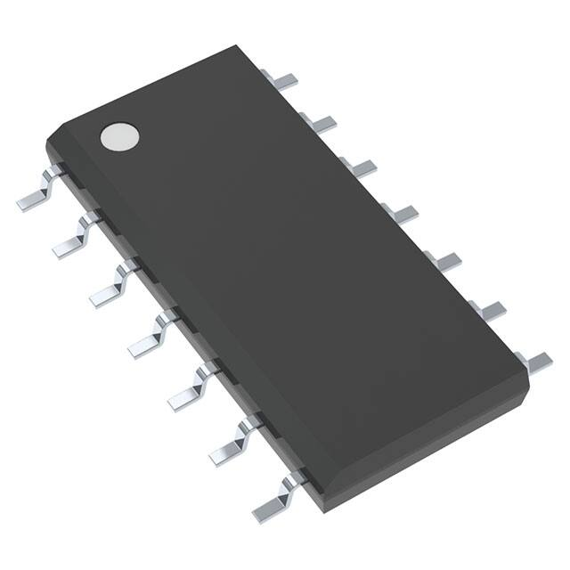


 工商网监
湘ICP备2023018690号
工商网监
湘ICP备2023018690号
