Is Now Part of
To learn more about ON Semiconductor, please visit our website at
www.onsemi.com
ON Semiconductor and the ON Semiconductor logo are trademarks of Semiconductor Components Industries, LLC dba ON Semiconductor or its subsidiaries in the United States and/or other countries. ON Semiconductor owns the rights to a number
of patents, trademarks, copyrights, trade secrets, and other intellectual property. A listing of ON Semiconductor’s product/patent coverage may be accessed at www.onsemi.com/site/pdf/Patent-Marking.pdf. ON Semiconductor reserves the right
to make changes without further notice to any products herein. ON Semiconductor makes no warranty, representation or guarantee regarding the suitability of its products for any particular purpose, nor does ON Semiconductor assume any liability
arising out of the application or use of any product or circuit, and specifically disclaims any and all liability, including without limitation special, consequential or incidental damages. Buyer is responsible for its products and applications using ON
Semiconductor products, including compliance with all laws, regulations and safety requirements or standards, regardless of any support or applications information provided by ON Semiconductor. “Typical” parameters which may be provided in ON
Semiconductor data sheets and/or specifications can and do vary in different applications and actual performance may vary over time. All operating parameters, including “Typicals” must be validated for each customer application by customer’s
technical experts. ON Semiconductor does not convey any license under its patent rights nor the rights of others. ON Semiconductor products are not designed, intended, or authorized for use as a critical component in life support systems or any FDA
Class 3 medical devices or medical devices with a same or similar classification in a foreign jurisdiction or any devices intended for implantation in the human body. Should Buyer purchase or use ON Semiconductor products for any such unintended
or unauthorized application, Buyer shall indemnify and hold ON Semiconductor and its officers, employees, subsidiaries, affiliates, and distributors harmless against all claims, costs, damages, and expenses, and reasonable attorney fees arising out
of, directly or indirectly, any claim of personal injury or death associated with such unintended or unauthorized use, even if such claim alleges that ON Semiconductor was negligent regarding the design or manufacture of the part. ON Semiconductor
is an Equal Opportunity/Affirmative Action Employer. This literature is subject to all applicable copyright laws and is not for resale in any manner.
�74VHC02
Quad 2-Input NOR Gate
Features
General Description
■ High Speed: tPD = 3.6ns (Typ.) at VCC = 5V
■ Low power dissipation: ICC = 2µA (Max.) at TA = 25°C
The VHC02 is an advanced high-speed CMOS 2-Input
NOR Gate fabricated with silicon gate CMOS technology. It achieves the high-speed operation similar to
equivalent Bipolar Schottky TTL while maintaining the
CMOS low power dissipation. The internal circuit is
composed of 3 stages, including buffer output, which
provide high noise immunity and stable output. An input
protection circuit insures that 0V to 7V can be applied to
the input pins without regard to the supply voltage. This
device can be used to interface 5V to 3V systems and
two supply systems such as battery backup. This circuit
prevents device destruction due to mismatched supply
and input voltages.
■ High noise immunity: VNIH = VNIL = 28% VCC (Min.)
■ Power down protection is provided on all inputs
■ Low noise: VOLP = 0.8V (Max.)
■ Pin and function compatible with 74HC02
Ordering Information
Order Number
Package
Number
Package Description
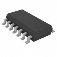
74VHC02M
M14A
14-Lead Small Outline Integrated Circuit (SOIC), JEDEC MS-012, 0.150"
Narrow
74VHC02SJ
M14D
14-Lead Small Outline Package (SOP), EIAJ TYPE II, 5.3mm Wide
74VHC02MTC
MTC14
14-Lead Thin Shrink Small Outline Package (TSSOP), JEDEC MO-153,
4.4mm Wide
Device also available in Tape and Reel. Specify by appending suffix letter “X” to the ordering number.
All packages are lead free per JEDEC: J-STD-020B standard.
©1992 Fairchild Semiconductor Corporation
74VHC02 Rev. 1.4.0
www.fairchildsemi.com
74VHC02 — Quad 2-Input NOR Gate
December 2007
�74VHC02 — Quad 2-Input NOR Gate
Connection Diagram
Logic Symbol
IEEE/IEC
Pin Description
Pin Names
Truth Table
Description
An, Bn
Inputs
A
On
Outputs
©1992 Fairchild Semiconductor Corporation
74VHC02 Rev. 1.4.0
B
O
L
L
H
L
H
L
H
L
L
H
H
L
www.fairchildsemi.com
2
�Symbol
Parameter
Rating
VCC
Supply Voltage
–0.5V to +7.0V
VIN
DC Input Voltage
–0.5V to +7.0V
VOUT
DC Output Voltage
–0.5V to VCC + 0.5V
IIK
Input Diode Current
–20mA
IOK
Output Diode Current
±20mA
IOUT
DC Output Current
±25mA
ICC
DC VCC / GND Current
TSTG
TL
±50mA
Storage Temperature
–65°C to +150°C
Lead Temperature (Soldering, 10 seconds)
260°C
Recommended Operating Conditions(1)
The Recommended Operating Conditions table defines the conditions for actual device operation. Recommended
operating conditions are specified to ensure optimal performance to the datasheet specifications. Fairchild does not
recommend exceeding them or designing to absolute maximum ratings.
Symbol
Parameter
VCC
Supply Voltage
VIN
Input Voltage
VOUT
Output Voltage
TOPR
Operating Temperature
tr , tf
Rating
2.0V to +5.5V
0V to +5.5V
0V to VCC
–40°C to +85°C
Input Rise and Fall Time,
VCC = 3.3V ± 0.3V
0ns/V ∼ 100ns/V
VCC = 5.0V ± 0.5V
0ns/V ∼ 20ns/V
Note:
1. Unused inputs must be held HIGH or LOW. They may not float.
©1992 Fairchild Semiconductor Corporation
74VHC02 Rev. 1.4.0
www.fairchildsemi.com
3
74VHC02 — Quad 2-Input NOR Gate
Absolute Maximum Ratings
Stresses exceeding the absolute maximum ratings may damage the device. The device may not function or be
operable above the recommended operating conditions and stressing the parts to these levels is not recommended.
In addition, extended exposure to stresses above the recommended operating conditions may affect device reliability.
The absolute maximum ratings are stress ratings only.
�TA = –40°C to
+85°C
TA = 25°C
Symbol
Parameter
VCC (V)
VIH
HIGH Level Input
Voltage
2.0
Conditions
Min.
1.50
3.0–5.5
0.7 x VCC
VIL
LOW Level Input
Voltage
VOH
HIGH Level
Output Voltage
3.0
LOW Level
Output Voltage
Min.
IOH = –50µA
2.0
1.9
2.9
3.0
2.9
4.4
4.5
4.4
IOH = –4mA
2.58
2.48
IOH = –8mA
3.94
3.80
VIN = VIH
or VIL
IOL = 50µA
4.5
3.0
4.5
IOL = 8mA
V
0.0
0.1
0.1
0.0
0.1
0.1
0.0
IOL = 4mA
V
0.3 x VCC
1.9
4.5
3.0
V
0.50
0.3 x VCC
VIN = VIH
or VIL
Units
0.7 x VCC
3.0
2.0
Max.
0.50
3.0–5.5
2.0
Max.
1.50
2.0
4.5
VOL
Typ.
0.1
0.1
0.36
0.44
V
0.36
0.44
IIN
Input Leakage
Current
0–5.5
VIN = 5.5V or GND
±0.1
±1.0
µA
ICC
Quiescent
Supply Current
5.5
VIN = VCC or GND
2.0
20.0
µA
Noise Characteristics
TA = 25°C
Symbol
Parameter
VCC (V)
Conditions
Typ.
Limits
Units
Quiet Output Maximum
Dynamic VOL
5.0
CL = 50pF
0.3
0.8
V
VOLV(2)
Quiet Output Minimum
Dynamic VOL
5.0
CL = 50pF
–0.3
–0.8
V
VIHD(2)
Minimum HIGH Level
Dynamic Input Voltage
5.0
CL = 50pF
3.5
V
VILD(2)
Maximum LOW Level
Dynamic Input Voltage
5.0
CL = 50pF
1.5
V
VOLP
(2)
Note:
2. Parameter guaranteed by design.
©1992 Fairchild Semiconductor Corporation
74VHC02 Rev. 1.4.0
www.fairchildsemi.com
4
74VHC02 — Quad 2-Input NOR Gate
DC Electrical Characteristics
�TA = –40°C
to +85°C
TA = 25°C
Symbol
tPHL, tPLH
Parameter
Propagation Delay
VCC (V)
Conditions
3.3 ± 0.3
5.0 ± 0.5
CIN
Input Capacitance
CPD
Power Dissipation
Capacitance
Typ.
Max.
Min.
Max.
Units
CL = 15pF
5.6
7.9
1.0
9.5
ns
CL = 50pF
8.1
11.4
1.0
13.0
CL = 15pF
3.6
5.5
1.0
6.5
CL = 50pF
5.1
7.5
1.0
8.5
4
10
VCC
(3)
= Open
Min.
10
15
ns
pF
pF
Note:
3. CPD is defined as the value of the internal equivalent capacitance which is calculated from the operating
current consumption without load. Average operating current can be obtained by the equation:
ICC (opr.) = CPD • VCC • fIN + ICC / 4 (per gate).
©1992 Fairchild Semiconductor Corporation
74VHC02 Rev. 1.4.0
www.fairchildsemi.com
5
74VHC02 — Quad 2-Input NOR Gate
AC Electrical Characteristics
�0.65
A
0.43TYP
14
8
B
6.4
6.10
3.2
1
PIN#1 IDENT
0.2 C B A
7
TOP VIEW
1.65
ALL LEAD TIPS
0.45
RECOMMENDED LAND PATTERN
1.2 MAX
0.30
0.19
ALL LEAD TIPS
0.1 C
0.65
SEE DETAIL A
0.90+0.15
-0.10
0.13
A B
0.20
0.09
C
C
FRONT VIEW
0.09 MIN
NOTES:
A. CONFORMS TO JEDEC REGISTRATION MO-153,
VARIATION AB, REF NOTE 6
B. DIMENSIONS ARE IN MILLIMETERS.
C. DIMENSIONS ARE EXCLUSIVE OF BURRS,
MOLD FLASH, AND TIE BAR EXTRUSIONS
D. DIMENSIONING AND TOLERANCES PER ANSI
Y14.5M, 2009.
E. LANDPATTERN STANDARD: SOP65P640X110-14M.
F. DRAWING FILE NAME: MKT-MTC14rev7.
GAGE PLANE
0.09 MIN
1.00
0.25
SEATING PLANE
DETAIL A
��8.75
8.50
A
7.62
14
8
14
B
0.65
8
4.00
3.80
6.00
1
PIN #1
IDENT.
1.27
(0.33)
TOP VIEW
5.60
7
0.51
0.35
0.25 M C B A
1.75 MAX
1.70
1
1.27
LAND PATTERN RECOMMENDATION
A
C
1.50
1.25
FRONT VIEW
0.25
0.10
0.50
0.25 x 45
R0.10
GAGE
PLANE
R0.10
0.36
8°
0°
0.90
0.50
(1.04)
0.10 C
0.25
0.19
SIDE VIEW
NOTES:
A. CONFORMS TO JEDEC MS-012,
VARIATION AB, ISSUE C
B. ALL DIMENSIONS ARE IN MILLIMETERS
C. DIMENSIONS DO NOT INCLUDE MOLD
FLASH OR BURRS
D. LAND PATTERN STANDARD:
SOIC127P600X145-14M
E. CONFORMS TO ASME Y14.5M, 2009
D. DRAWING FILENAME: MKT-M14Arev14
SEATING PLANE
DETAIL A
SCALE 16 : 1
7
�ON Semiconductor and
are trademarks of Semiconductor Components Industries, LLC dba ON Semiconductor or its subsidiaries in the United States and/or other countries.
ON Semiconductor owns the rights to a number of patents, trademarks, copyrights, trade secrets, and other intellectual property. A listing of ON Semiconductor’s product/patent
coverage may be accessed at www.onsemi.com/site/pdf/Patent−Marking.pdf. ON Semiconductor reserves the right to make changes without further notice to any products herein.
ON Semiconductor makes no warranty, representation or guarantee regarding the suitability of its products for any particular purpose, nor does ON Semiconductor assume any liability
arising out of the application or use of any product or circuit, and specifically disclaims any and all liability, including without limitation special, consequential or incidental damages.
Buyer is responsible for its products and applications using ON Semiconductor products, including compliance with all laws, regulations and safety requirements or standards,
regardless of any support or applications information provided by ON Semiconductor. “Typical” parameters which may be provided in ON Semiconductor data sheets and/or
specifications can and do vary in different applications and actual performance may vary over time. All operating parameters, including “Typicals” must be validated for each customer
application by customer’s technical experts. ON Semiconductor does not convey any license under its patent rights nor the rights of others. ON Semiconductor products are not
designed, intended, or authorized for use as a critical component in life support systems or any FDA Class 3 medical devices or medical devices with a same or similar classification
in a foreign jurisdiction or any devices intended for implantation in the human body. Should Buyer purchase or use ON Semiconductor products for any such unintended or unauthorized
application, Buyer shall indemnify and hold ON Semiconductor and its officers, employees, subsidiaries, affiliates, and distributors harmless against all claims, costs, damages, and
expenses, and reasonable attorney fees arising out of, directly or indirectly, any claim of personal injury or death associated with such unintended or unauthorized use, even if such
claim alleges that ON Semiconductor was negligent regarding the design or manufacture of the part. ON Semiconductor is an Equal Opportunity/Affirmative Action Employer. This
literature is subject to all applicable copyright laws and is not for resale in any manner.
PUBLICATION ORDERING INFORMATION
LITERATURE FULFILLMENT:
Literature Distribution Center for ON Semiconductor
19521 E. 32nd Pkwy, Aurora, Colorado 80011 USA
Phone: 303−675−2175 or 800−344−3860 Toll Free USA/Canada
Fax: 303−675−2176 or 800−344−3867 Toll Free USA/Canada
Email: orderlit@onsemi.com
© Semiconductor Components Industries, LLC
N. American Technical Support: 800−282−9855 Toll Free
USA/Canada
Europe, Middle East and Africa Technical Support:
Phone: 421 33 790 2910
Japan Customer Focus Center
Phone: 81−3−5817−1050
www.onsemi.com
1
ON Semiconductor Website: www.onsemi.com
Order Literature: http://www.onsemi.com/orderlit
For additional information, please contact your local
Sales Representative
www.onsemi.com
�


 工商网监
湘ICP备2023018690号
工商网监
湘ICP备2023018690号
