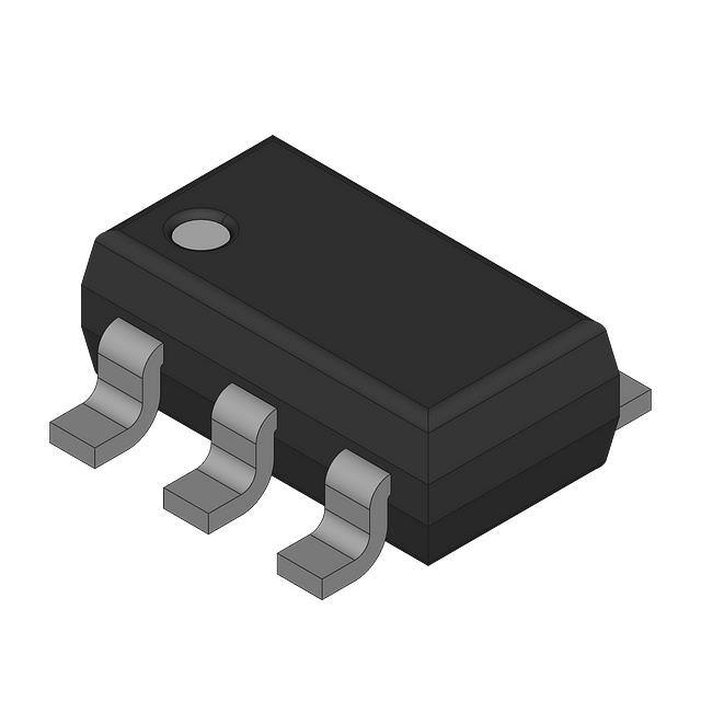
7WB3305
2-Bit Bus Switch
The 7WB3305 is an advanced high−speed low−power 2−bit bus
switch in ultra−small footprints.
Features
•
•
•
•
•
•
•
High Speed: tPD = 0.25 ns (Max) @ VCC = 4.5 V
3 W Switch Connection Between 2 Ports
Power Down Protection Provided on Inputs
Zero Bounce
TTL−Compatible Control Inputs
Ultra−Small Pb−Free Packages
These are Pb−Free Devices
http://onsemi.com
MARKING
DIAGRAMS
8
1
UDFN8
MU SUFFIX
CASE 517AJ
AMM
G
8
Micro8]
DM SUFFIX
CASE 846A
3305
AYWG
G
1
UDFN8
1.95 x 1.0
CASE 517CA
A
Y
W
M
G
XM
1
= Assembly Location
= Year
= Work Week
= Date Code
= Pb−Free Package
(Note: Microdot may be in either location)
ORDERING INFORMATION
See detailed ordering and shipping information in the package
dimensions section on page 7 of this data sheet.
© Semiconductor Components Industries, LLC, 2014
October, 2014 − Rev. 1
1
Publication Order Number:
7WB3305/D
�7WB3305
OE1
1
8
VCC
A1
2
7
OE2
B1
3
6
OE1
1
8
VCC
A1
2
7
OE2
B1
3
6
B2
GND
4
5
A2
B2
Figure 2. Micro8
(Top View)
GND
4
5
A2
Figure 1. UDFN8
(Top Thru−View)
A1
B1
FUNCTION TABLE
OE1
A2
B2
OE2
Figure 3. Logic Diagram
http://onsemi.com
2
Input OEn
Function
L
Disconnect
H
Bn = An
�7WB3305
MAXIMUM RATINGS
Symbol
Value
Unit
VCC
DC Supply Voltage
Parameter
−0.5 to +7.0
V
VIN
Control Pin Input Voltage
−0.5 to +7.0
V
VI/O
Switch Input / Output Voltage
−0.5 to +7.0
V
IIK
Control Pin DC Input Diode Current
VIN < GND
−50
mA
IOK
Switch I/O Port DC Diode Current
VI/O < GND
−50
mA
IO
ON−State Switch Current
$128
mA
Continuous Current Through VCC or GND
$150
mA
ICC
DC Supply Current Per Supply Pin
$150
mA
IGND
DC Ground Current per Ground Pin
$150
mA
TSTG
Storage Temperature Range
−65 to +150
°C
260
°C
TL
Lead Temperature, 1 mm from Case for 10 Seconds
TJ
Junction Temperature Under Bias
qJA
Thermal Resistance
PD
Power Dissipation in Still Air at 85°C
MSL
FR
VESD
ILATCHUP
150
°C
UDFN8 (Note 1)
Micro8
111
392
°C/W
UDFN8
Micro8
1127
319
mW
Moisture Sensitivity
Level 1
Flammability Rating Oxygen Index: 28 to 34
ESD Withstand Voltage
UL 94 V−0 @ 0.125 in
Human Body Mode (Note 2)
Machine Model (Note 3)
Charged Device Model (Note 4)
> 2000
> 200
N/A
V
$200
mA
Latchup Performance Above VCC and Below GND at 125°C (Note 5)
Stresses exceeding those listed in the Maximum Ratings table may damage the device. If any of these limits are exceeded, device functionality
should not be assumed, damage may occur and reliability may be affected.
1. Measured with minimum pad spacing on an FR4 board, using 10 mm−by−1 inch, 2 ounce copper trace no air flow.
2. Tested to EIA / JESD22−A114−A.
3. Tested to EIA / JESD22−A115−A.
4. Tested to JESD22−C101−A.
5. Tested to EIA / JESD78.
RECOMMENDED OPERATING CONDITIONS
Symbol
Parameter
Min
Max
Unit
4.0
5.5
V
VCC
Positive DC Supply Voltage
VIN
Control Pin Input Voltage
0
5.5
V
VI/O
Switch Input / Output Voltage
0
5.5
V
−55
+125
°C
0
0
5
DC
nS/V
TA
Operating Free−Air Temperature
Dt/DV
Input Transition Rise or Fall Rate
Control Input
Switch I/O
Functional operation above the stresses listed in the Recommended Operating Ranges is not implied. Extended exposure to stresses beyond
the Recommended Operating Ranges limits may affect device reliability.
http://onsemi.com
3
�7WB3305
DC ELECTRICAL CHARACTERISTICS
Symbol
Parameter
VCC
(V)
Conditions
Min
Typ
4.5
Max
Min
−1.2
Max
Unit
−1.2
V
VIK
Clamp Diode Voltage
VIH
High−Level Input Voltage
(Control)
4.0 to
5.5
VIL
Low−Level Input Voltage
(Control)
4.0 to
5.5
0.8
0.8
V
VOH
Output Voltage High
See Figure 4
Input Leakage Current
0 v VIN v 5.5 V
5.5
$0.1
$1.0
mA
IOFF
Power Off Leakage Current
VI/O = 0 to 5.5 V
0
$0.1
$1.0
mA
ICC
Quiescent Supply Current
IO = 0,
VIN = VCC or 0 V
5.5
$0.1
$1.0
mA
DICC
Increase in Supply Current
(Control Pin)
One input at 3.4 V;
Other inputs at
VCC or GND
5.5
2.5
mA
RON
Switch ON Resistance
VI/O = 0,
II/O = 64 mA
II/O = 30 mA
4.5
IIN
II/O = −18 mA
TA =
−555C to +1255C
TA = 255C
2.0
V
W
VI/O = 2.4,
II/O = 15 mA
VI/O = 2.4,
II/O = 15 mA
2.0
3
3
7
7
7
7
6
15
15
10
20
20
4.0
Product parametric performance is indicated in the Electrical Characteristics for the listed test conditions, unless otherwise noted. Product
performance may not be indicated by the Electrical Characteristics if operated under different conditions.
AC ELECTRICAL CHARACTERISTICS
Symbol
Parameter
VCC
(V)
Test Condition
TA =
−555C to +1255C
TA = 25 5C
Min
Typ
Max
Min
Unit
0.25
ns
ns
tPD
Propagation Delay,
Bus to Bus
See Figure 5
4.0 to
5.5
tEN
Output Enable Time
See Figure 5
4.5 to
5.5
0.8
2.5
4.2
0.8
4.2
4.0
0.8
3.0
4.6
0.8
4.6
4.5 to
5.5
0.8
3.0
4.8
0.8
4.8
4.0
0.8
2.9
4.4
0.8
4.4
tDIS
CIN
Output Disable Time
0.25
Max
ns
Control Input Capacitance
VIN = 5 or 0 V
5.0
2.5
pF
CIO(ON)
Switch On Capacitance
Switch ON
5.0
10
pF
CIO(OFF)
Switch Off Capacitance
Switch OFF
5.0
5
pF
http://onsemi.com
4
�7WB3305
TYPICAL DC CHARACTERISTICS
VOH, HIGH LEVEL OUTPUT VOLTAGE (V)
4.50
4.25
−6 mA
4.00
−12 mA
3.75
IOH =
−0.1 mA
3.50
3.25
−24 mA
3.00
2.75
TA = +85°C
VIN = VCC
2.50
2.25
4.00
4.25
4.75
5.25
5.00
5.50
5.75
5.60
VCC, SUPPLY VOLTAGE (V)
VOH, HIGH LEVEL OUTPUT VOLTAGE (V)
4.50
4.25
−6 mA
−12 mA
4.00
3.75
IOH =
−0.1 mA
3.50
3.25
−24 mA
3.00
2.75
TA = +25°C
VIN = VCC
2.50
2.25
4.00
4.25
4.75
5.25
5.00
5.50
5.75
5.60
VCC, SUPPLY VOLTAGE (V)
VOH, HIGH LEVEL OUTPUT VOLTAGE (V)
4.50
4.25
−6 mA
4.00
−12 mA
3.75
IOH =
−0.1 mA
3.50
3.25
−24 mA
3.00
2.75
TA = −40°C
VIN = VCC
2.50
2.25
4.00
4.25
4.75
5.25
5.00
5.50
5.75
5.60
VCC, SUPPLY VOLTAGE (V)
Figure 4. Output Voltage High vs Supply Voltage
http://onsemi.com
5
�7WB3305
AC LOADING AND WAVEFORMS
Parameter Measurement Information
From Output
Under Test
500 W
S1
7V
Test
S1
tPD
Open
tPLZ/tPZL
7V
tPHZ/tPZH
Open
Open
GND
CL = 50 pF*
500 W
*CL includes probes and jig capacitance.
1.5 V
1.5 V
Output
Control
3V
Input
tPHL
VOH
1.5 V
1.5 V
Output
1.5 V
Output
Waveform 2
S1 at Open
(Note 6)
VOL
Voltage Waveforms
Propagation Delay Times
1.5 V
3V
0V
tPLZ
tPZL
Output
Waveform 1
S1 at 7 V
(Note 6)
tPZH
0V
tPLH
1.5 V
1.5 V
3.5 V
VOL + 0.3 V
VOL
tPHZ
VOH
VOH − 0.3 V
0V
Voltage Waveforms
Enable and Disable Times
6. Waveform 1 is for an output with internal conditions such that the output is low, except when disabled by the output control.
Waveform 2 is for an output with internal conditions such that the output is high, except when disabled by the output control
7. All input pulses are supplied by generators having the following characteristics: PRR v 10 MHz, ZO = 50 W, tr v 2.5 ns, tf v 2.5 ns.
8. The outputs are measured one at a time, with one transition per measurement.
9. tPLZ and tPHZ are the same as tDIS.
10. tPZL and tPZH are the same as tEN.
11. tPHL and tPLH are the same as tPD.
Figure 5. tPD, tEN, tDIS Loading and Waveforms
http://onsemi.com
6
�7WB3305
ORDERING INFORMATION
Package
Shipping†
7WB3305MUTAG
UDFN8
(Pb−Free)
3000 / Tape & Reel
7WB3305DMR2G
Micro8
(Pb−Free)
4000 / Tape & Reel
UDFN8, 1.95 x 1.0, 0.5 mm Pitch
(Pb−Free)
3000 / Tape & Reel
Device
7WB3305DMUTCG
†For information on tape and reel specifications, including part orientation and tape sizes, please refer to our Tape and Reel Packaging
Specifications Brochure, BRD8011/D.
http://onsemi.com
7
�MECHANICAL CASE OUTLINE
PACKAGE DIMENSIONS
UDFN8 1.8x1.2, 0.4P
CASE 517AJ−01
ISSUE O
8
1
DATE 08 NOV 2006
SCALE 4:1
A B
D
ÉÉ
ÉÉ
0.10 C
PIN ONE
REFERENCE
0.10 C
L1
E
DETAIL A
NOTE 5
TOP VIEW
(A3)
0.05 C
DIM
A
A1
A3
b
b2
D
E
e
L
L1
L2
A
0.05 C
SIDE VIEW
e/2
(b2)
A1
e
1
4
8
5
C
SEATING
PLANE
DETAIL A
8X
L
8X b
0.10
M
C A B
0.05
M
C
NOTE 3
MOUNTING FOOTPRINT
SOLDERMASK DEFINED
8X
0.66
7X
0.22
MILLIMETERS
MIN
MAX
0.45
0.55
0.00
0.05
0.127 REF
0.15
0.25
0.30 REF
1.80 BSC
1.20 BSC
0.40 BSC
0.45
0.55
0.00
0.03
0.40 REF
GENERIC
MARKING DIAGRAM*
(L2)
BOTTOM VIEW
NOTES:
1. DIMENSIONING AND TOLERANCING PER
ASME Y14.5M, 1994.
2. CONTROLLING DIMENSION: MILLIMETERS.
3. DIMENSION b APPLIES TO PLATED
TERMINAL AND IS MEASURED BETWEEN
0.15 AND 0.30 mm FROM TERMINAL TIP.
4. MOLD FLASH ALLOWED ON TERMINALS
ALONG EDGE OF PACKAGE. FLASH MAY
NOT EXCEED 0.03 ONTO BOTTOM
SURFACE OF TERMINALS.
5. DETAIL A SHOWS OPTIONAL
CONSTRUCTION FOR TERMINALS.
XXM
G
XX = Specific Device Code
M = Date Code
G
= Pb−Free Package
*This information is generic. Please refer to
device data sheet for actual part marking.
Pb−Free indicator, “G” or microdot “ G”,
may or may not be present.
1.50
1
0.32
0.40 PITCH
DIMENSIONS: MILLIMETERS
DOCUMENT NUMBER:
DESCRIPTION:
98AON23417D
UDFN8 1.8X1.2, 0.4P
Electronic versions are uncontrolled except when accessed directly from the Document Repository.
Printed versions are uncontrolled except when stamped “CONTROLLED COPY” in red.
PAGE 1 OF 1
ON Semiconductor and
are trademarks of Semiconductor Components Industries, LLC dba ON Semiconductor or its subsidiaries in the United States and/or other countries.
ON Semiconductor reserves the right to make changes without further notice to any products herein. ON Semiconductor makes no warranty, representation or guarantee regarding
the suitability of its products for any particular purpose, nor does ON Semiconductor assume any liability arising out of the application or use of any product or circuit, and specifically
disclaims any and all liability, including without limitation special, consequential or incidental damages. ON Semiconductor does not convey any license under its patent rights nor the
rights of others.
© Semiconductor Components Industries, LLC, 2019
www.onsemi.com
�onsemi,
, and other names, marks, and brands are registered and/or common law trademarks of Semiconductor Components Industries, LLC dba “onsemi” or its affiliates
and/or subsidiaries in the United States and/or other countries. onsemi owns the rights to a number of patents, trademarks, copyrights, trade secrets, and other intellectual property.
A listing of onsemi’s product/patent coverage may be accessed at www.onsemi.com/site/pdf/Patent−Marking.pdf. onsemi reserves the right to make changes at any time to any
products or information herein, without notice. The information herein is provided “as−is” and onsemi makes no warranty, representation or guarantee regarding the accuracy of the
information, product features, availability, functionality, or suitability of its products for any particular purpose, nor does onsemi assume any liability arising out of the application or use
of any product or circuit, and specifically disclaims any and all liability, including without limitation special, consequential or incidental damages. Buyer is responsible for its products
and applications using onsemi products, including compliance with all laws, regulations and safety requirements or standards, regardless of any support or applications information
provided by onsemi. “Typical” parameters which may be provided in onsemi data sheets and/or specifications can and do vary in different applications and actual performance may
vary over time. All operating parameters, including “Typicals” must be validated for each customer application by customer’s technical experts. onsemi does not convey any license
under any of its intellectual property rights nor the rights of others. onsemi products are not designed, intended, or authorized for use as a critical component in life support systems
or any FDA Class 3 medical devices or medical devices with a same or similar classification in a foreign jurisdiction or any devices intended for implantation in the human body. Should
Buyer purchase or use onsemi products for any such unintended or unauthorized application, Buyer shall indemnify and hold onsemi and its officers, employees, subsidiaries, affiliates,
and distributors harmless against all claims, costs, damages, and expenses, and reasonable attorney fees arising out of, directly or indirectly, any claim of personal injury or death
associated with such unintended or unauthorized use, even if such claim alleges that onsemi was negligent regarding the design or manufacture of the part. onsemi is an Equal
Opportunity/Affirmative Action Employer. This literature is subject to all applicable copyright laws and is not for resale in any manner.
PUBLICATION ORDERING INFORMATION
LITERATURE FULFILLMENT:
Email Requests to: orderlit@onsemi.com
onsemi Website: www.onsemi.com
◊
TECHNICAL SUPPORT
North American Technical Support:
Voice Mail: 1 800−282−9855 Toll Free USA/Canada
Phone: 011 421 33 790 2910
Europe, Middle East and Africa Technical Support:
Phone: 00421 33 790 2910
For additional information, please contact your local Sales Representative
�


 工商网监
湘ICP备2023018690号
工商网监
湘ICP备2023018690号
