ON Semiconductor
Is Now
To learn more about onsemi™, please visit our website at
www.onsemi.com
onsemi and and other names, marks, and brands are registered and/or common law trademarks of Semiconductor Components Industries, LLC dba “onsemi” or its affiliates and/or
subsidiaries in the United States and/or other countries. onsemi owns the rights to a number of patents, trademarks, copyrights, trade secrets, and other intellectual property. A listing of onsemi
product/patent coverage may be accessed at www.onsemi.com/site/pdf/Patent-Marking.pdf. onsemi reserves the right to make changes at any time to any products or information herein, without
notice. The information herein is provided “as-is” and onsemi makes no warranty, representation or guarantee regarding the accuracy of the information, product features, availability, functionality,
or suitability of its products for any particular purpose, nor does onsemi assume any liability arising out of the application or use of any product or circuit, and specifically disclaims any and all
liability, including without limitation special, consequential or incidental damages. Buyer is responsible for its products and applications using onsemi products, including compliance with all laws,
regulations and safety requirements or standards, regardless of any support or applications information provided by onsemi. “Typical” parameters which may be provided in onsemi data sheets and/
or specifications can and do vary in different applications and actual performance may vary over time. All operating parameters, including “Typicals” must be validated for each customer application
by customer’s technical experts. onsemi does not convey any license under any of its intellectual property rights nor the rights of others. onsemi products are not designed, intended, or authorized
for use as a critical component in life support systems or any FDA Class 3 medical devices or medical devices with a same or similar classification in a foreign jurisdiction or any devices intended for
implantation in the human body. Should Buyer purchase or use onsemi products for any such unintended or unauthorized application, Buyer shall indemnify and hold onsemi and its officers, employees,
subsidiaries, affiliates, and distributors harmless against all claims, costs, damages, and expenses, and reasonable attorney fees arising out of, directly or indirectly, any claim of personal injury or death
associated with such unintended or unauthorized use, even if such claim alleges that onsemi was negligent regarding the design or manufacture of the part. onsemi is an Equal Opportunity/Affirmative
Action Employer. This literature is subject to all applicable copyright laws and is not for resale in any manner. Other names and brands may be claimed as the property of others.
�AMIS-492x0
AMIS-492x0 Fieldbus MAU
Overview
AMIS−492x0 Fieldbus MAU (Media Access Unit) is a transceiver
chip for low speed FOUNDATION® Fieldbus and Profibus PA
devices. The AMIS−49200 was originally designed to be a near
pin-for-pin replacement of the Yokogawa mSAA22Q MAU. “Near
pin-for-pin” means that associated component values may change, but
no board changes are required. A micro-leadframe package option
(NQFP) is also available, the AMIS−49250.
www.onsemi.com
Features
AMIS−492x0 Fieldbus MAU is a transceiver IC for low speed
FOUNDATION Fieldbus and Profibus PA devices. It incorporates the
following features:
• All Node Power can be Supplied by the Bus, via the AMIS-492x0
• Current Consumption 500 mA (Typ)
• VCC Voltage: 6.2 V to 4.75 V
• VDD Voltage: 5.5 V to 2.7 V
• Compatible to IEC 1158−2 and ISA 50.02
• Shunt Regulator
• Voltage Reference (Internal Only)
• Series Regulator
• Band-pass Filter
• Slew Rate Control
• Segment Current Control
• Low Voltage Detection
• Carrier Detect
• Data Rate: 31.25 kbps Voltage Mode
• Dual Voltage Supply 3−6.2 V
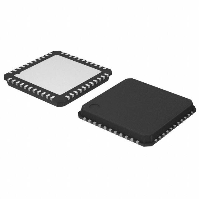
• 44-pin LQFP/NQFP Package
• These Devices are Pb−Free and are RoHS Compliant
LQFP−44, 10x10
CASE 561AA
NQFP 44, 7x7
CASE 560BD
ORDERING INFORMATION
See detailed ordering and shipping information in the package
dimensions section on page 15 of this data sheet.
Applications
• Process Automation
• Pressure and Temperature Monitoring
Definitions, Acronyms and Abbreviations
IC
ESD
FF
LQFP
Manchester
MAU
MDS
NQFP
mSAA22Q
− Integrated Circuit
− Electrostatic Discharge
− FOUNDATION Fieldbus
− Low Profile Quad Flat Pack
− Communications Encoding Scheme Implemented in
FOUNDATION Fieldbus
− Medium Attachment Unit
− Medium Dependent Sub-layer
− “Near Chip-scale” Quad Flat Pack
− Name of Yokogawa’s MAU IC
© Semiconductor Components Industries, LLC, 2016
August, 2016 − Rev. 8
1
Publication Order Number:
AMIS−492x0/D
�AMIS−492x0
Block Diagram
33
VSS
Receive Block
35
RXS
31
30
FLTOUT
FLT
HPF
Zero-cross
Detector
SIGIN
Bandpass Filter
34
32
RXA
LPF
Carrier
Detector
28
27
29
CCD
Transmit Block
36
37
1
41
42
43
39
40
POL
MDS
Interface
TXE
VSS
VSS
VSS
CCINP
VSS
Current
Driver
VSS
VSS
Power Supply Block
VSS
VCC
Basic
Circuitry
18
CCOUT
Vmid
Reference
VCC
VCC
CCINM
VCC
VSS
VCC
11
15
14
5
SHSETIN
SRSETIN
12
N_PFail1
SRTR
SRAO
VSS
N_PFail2
SRSET
Shunt
Regulator
Low Voltage
Detectors
Series
Regulator
20
22
23
24
25
3
2
Vref
4
SHSET
VO
19
Vmid
Vref
Bandgap
VCC
17
21
Vmid
VDD
13
CRT
TXS
44
16
VDRV
Tri-level Modulator
&
Slew Control
SHUNT
38
6
7
8
SGND
26
MDS_CTRL
9
VSS
10
Figure 1. AMIS−492x0 Fieldbus MAU Block Diagram
Table 1. PIN NUMBERS AND SIGNAL DESCRIPTION
Signal
Name
Pin
No.
I/O
(Note 1)
Description
VSS
1
Ground
VREF
2
AO
Connect to Ground.
Internal bandgap voltage (1.18 V).
VMID
3
AO
2 V bias voltage for AC signals.
N_PFAIL1
4
AI/O
Power fail alarm at VCC input. This pin is an open-drain output of negative logic.
N_PFAIL2
5
AI/O
Power fail alarm at VDD input. This pin is an open-drain output of negative logic.
SHSETIN
6
AI
Feedback (non-inverting) input for the shunt regulator.
SHSET
7
AO
Divided voltage of VCC input. Feeding this voltage to SHSETIN pin results in 5 V voltage at VCC.
1. AI = Analog Input, AO = Analog Output, AI/O = Analog Input/Output, DIS = CMOS Digital Input (Schmitt Trigger), DO = CMOS Digital
Output.
www.onsemi.com
2
�AMIS−492x0
Table 1. PIN NUMBERS AND SIGNAL DESCRIPTION (continued)
Signal
Name
Pin
No.
I/O
(Note 1)
SHUNT
8
AI
Control pin of the shunt regulator. Its sink current (25 mA max) is controlled so that the voltage at
SHSETIN is equal to VREF (1.18 V).
VSS/SGND
9
Ground
The Current absorbed by SHUNT pin (25 mA max) is fed to this pin, which must be connected to
the ground level.
VSS
10
Ground
Ground
VSS
11
Ground
Ground
SRSETIN
12
AI
Feedback (inverting) input for the series regulator. The series regulator controls its output (SRAO)
to make this input voltage is equal to VREF (1.18 V).
SRSET
13
AO
Divided voltage of VO output. Feeding this voltage into SRSETIN pin results in 3 V at VO pin.
SRAO
14
AO
Output pin of an operational amplifier for the series regulator.
SRTR
15
AI
Gate of a PMOS transistor for the series regulator.
VO
16
AO
Output pin of the series regulator (20 mA max).
VDD
17
Digital Supply
Supply voltage input for digital block.
VCC
18
Analog Supply
Analog supply voltage.
CRT
19
AI/O
VSS
20
Ground
VDRV
21
AO
VSS
22
Ground
CCINP
23
AI
Non-inverting input of an operational amplifier for transmission current driver.
Description
Current integration to limit output slew rate.
Ground
Output of an operational amplifier for slew rate control. This signal can be fed to current driver.
Ground
CCINM
24
AI
Inverting input of an operational amplifier for transmission current driver.
CCOUT
25
AO
Output of an operational amplifier for transmission current driver.
MDS_CTRL
26
AI
For POL = VDD MDS_CTRL should = VSS
For POL = VSS MDS_CTRL can be tied to VDD or used as a not reset to control when transmit
communications will be enabled.
SIGIN
27
AI
Input pin of the band-pass filter. This pin si connected to VMID bias level with 270 kW resistor.
HPF
28
AI
Feedback signal of high-pass filter. This pin si connected to the output of an op-amp for high pass
filter with 75 kW resistor.
LPF
29
AI
Non-inverting input of an operational amplifier for the low-pass filter.
FLT
30
AI
Input pin of low-pass filter for feedback. This pin is connected to the output of the high-pass filter
through 20 kW and the non-inverting input of the low-pass filter through 54 kW resisters.
FLTOUT
31
AO
Output of the operational amplifier for the low-pass filter. This signal is internally connected to
non-inverting input to form a voltage-follower.
CCD
32
AO
Current integration (for carrier detect circuit).
VSS
33
Ground
RXA
34
DO
MDS−MAU interface signal for received signal activity. This pin is a push-pull output.
RXS
35
DO
MDS−MAU interface signal for received signal. This pin is a push-pull output.
TXE
36
DIS
MDS−MAU interface signal for enable signal transmission (Schmitt Trigger input).
TXS
37
DIS
MDS−MAU interface signal for signal to be transmitted (Schmitt Trigger input).
POL
38
DIS
Selects polarity of TxE input. When this pin is connected to GND, TxE is active high. When this pin
is connected to VDD, TxE is active low.
VSS
39
Ground
Ground
VSS
40
Ground
Ground
VSS
41
Ground
Connect to ground.
VSS
42
Ground
Connect to ground.
VSS
43
Ground
Connect to ground.
VCC
44
Analog Supply
Ground
Analog supply voltage.
1. AI = Analog Input, AO = Analog Output, AI/O = Analog Input/Output, DIS = CMOS Digital Input (Schmitt Trigger), DO = CMOS Digital
Output.
www.onsemi.com
3
�AMIS−492x0
ELECTRICAL CHARACTERISTICS
Operating Conditions
Unless otherwise noted, all block and sub-block specifications apply over the operating temperature (−40 to +85°C).
Table 2. ABSOLUTE MAXIMUM RATINGS
Parameter
Symbol
Conditions
Min
Max
Unit
Analog Block Supply Voltage
VCC
−0.3
6.5
V
Digital Block Supply Voltage
VDD
−0.3
6.0
V
(TxS, TxE and POL Pins)
−0.3
VDD + 0.3
V
(RxS and RxA Pins)
−0.3
VDD + 0.3
V
Digital Input Pin Voltage
VIN
Digital Output Pin Voltage
VOUT
Not for Shunt Pin
−
±5
mA
For Shunt, SGND and VO
−
30
mA
ESD, Human Body Model
−
2,250
V
ESD, Machine Model
−
250
V
−
1,000
V
−55
125
°C
Input Pin Current
IIN
Output Pin Current
IOUT
ESD, Charged Device Model
Storage Temperature
TStorage
Stresses exceeding those listed in the Maximum Ratings table may damage the device. If any of these limits are exceeded, device functionality
should not be assumed, damage may occur and reliability may be affected.
Table 3. NORMAL OPERATING CONDITIONS
Parameter
Analog Supply Voltage
Symbol
VCC
Digital Supply Voltage
VDD
Storage Temperature
TOperating
Current Consumption
ICC
Conditions
Supply voltages are configurable,
or can be supplied from off-chip.
Min
Typ
Max
Unit
4.75
5
6.2
V
2.7
3
VCC − 1.1
V
−40
−
85
°C
−
500
800
mA
Symbol
Min
Max
Unit
Input High Voltage
VIH
0.7 × VDD
VDD
V
Input Low Voltage
VIL
0
0.3 × VDD
V
Input High Current
IIH
−
1
mA
Input Low Current
IIL
−
−1
mA
Schmitt Negative Threshold
Vt−
0.2 × VDD
−
V
Schmitt Positive Threshold
Vt+
−
0.8 × VDD
V
Schmitt Hysteresis
Vh
1
−
V
25°C, SHUNT current = 1 mA,
no current from series regulator.
Table 4. CMOS INPUT SPECIFICATIONS
Parameter
www.onsemi.com
4
�AMIS−492x0
Power Supply Blocks
Table 5. REGULATOR SPECIFICATIONS
Parameter
Symbol
Conditions
Min
Typ
Max
Unit
Preset, ISH = 1 to 5 mA
4.85
5.0
5.15
V
External Setting
4.75
−
6.2
V
Internal Pass Transistor N-ch and Pad
0.001
−
25
mA
5
−
−
mF
ISH = 1 to 25 mA
0
1.6
4
%
No Load Capacitance
−
−
±200
ppm/°C
Shunt Regulator
Output Voltage
VCC
Sink Current
ISH
Load Capacitance
CSH
Load Regulation
Temperature Coefficient
TCVcc
Series Regulator
Input Voltage
VCC
Internally Tied to VCC Pin
4.75
−
6.2
V
Output Voltage
VO
Preset, ISR = 0
2.91
3.0
3.09
V
External Setting and N-JFET
2.85
−
3.5
V
Output Current
ISR
Internal Pass Transistor P-ch and Pad
−
−
20
mA
Load Capacitance
CSR
For Stability use CAP w/ESR
5
−
−
mF
ISR = 0 to 20 mA
0
2
4
%
−
±200
−
ppm/°C
85
90
95
% Vref
0.012
0.025
0.038
V
VOL = 0.4 V (Open Drain)
30
−
135
mA
VOH = 5 V
−
−
1
mA
Min
Typ
Max
Unit
1.157
1.185
1.205
V
−
50
−
ppm/°C
−
100
−
mV
4.75
5
6.2
V
−
−
0
mA
Load Regulation
Temperature Coefficient
TCVo
Low Voltage Detectors (Applies to N_PFail1 and PFail2)
Threshold
VTH9
SxSETIN > VTH9 (Output: L → H)
Hysteresis
VHYS5
SxSETIN < (VTH9 − VHYS5)
(Output: H → L)
Output Sink Current
Output Leakage Current
IOL
IL
Table 6. VOLTAGE REFERENCE SPECIFICATIONS
Parameter
Symbol
Conditions
Bandgap Voltage Reference
Output Voltage Tolerance
VREF
Equates to: ±2%
Temperature Drift
Hysteresis
VREFHYS
Supply Voltage
VCCREF
Load Current
IREFOUT
(Note 2)
No Load During Operation
VMID Voltage Reference
Output Voltage
VMID
1.95
2.0
2.05
V
Output Current
IMID
−30
−
100
mA
Load Capacitance
CMID
0.01
0.1
1
mF
−
−
±200
ppm/°C
Temperature Coefficient
DVC6000F Uses 1 mF
TCMID
2. Hysteresis is defined as the change in the 25°C reading after 85°C to 25°C cycle and –40°C to 25°C cycle.
www.onsemi.com
5
�AMIS−492x0
Transmitter Blocks
Table 7. MDS−MAU INTERFACE
Parameter
Symbol
Min
Typ
Max
Unit
POL Input Pin
POL
See Schmitt Trigger Input Specs
V
TxE Input Pin
TxE
See Schmitt Trigger Input Specs
V
TxS input Pin
TxS
See Schmitt Trigger Input Specs
V
NOTE: The associated MDS chip must handle the jabber detect function.
Table 8. TRI-LEVEL MODULATOR
Parameter
Symbol
Conditions
Min
Typ
Max
Unit
VMID
−
3.02
V
−35
−
+120
mA
VMID + 0.485
VMID + 0.500
VMID + 0.515
V
Tri-level Modulator and Slew Control (Output is at VDRV)
Output Voltage
VO
Load Current
IO
⎪DV⎪ 10 mV
Output for Silence (Note 3)
VS
TXE Disabled
Output for High Level (Note 3)
VH
TXE Active
VS + 0.380
VS + 0.400
VS + 0.420
V
VL
TXE Active
VS − 0.420
VS − 0.400
VS − 0.380
V
−0.02
−
0.02
V
−
4.7
−
msec
Output for Low Level (Note 3)
Asymmetry of VH and VL
Rise and Fall Times (Note 4)
DVHL
tf, tr
CRT = 22 pF (Note 4)
3. Nominal values are: VS = 2.5 V, VH = 2.9 V and VL = 2.1 V.
4. By adding an external capacitor between the CRT pin and ground, slew rate at VDRV output can be controlled. The controlling equation is
tf or tr = 2 ms + (0.123 ms/pF * CRT). CRT is nominally 22 pF, yielding tf = tr = 4.7 ms. The constant comes from an internal capacitor. The hot
side of the capacitor and the CRT pin should have a guard pattern around them to avoid unnecessary interference.
Table 9. CURRENT CONTROL AMPLIFIER
Parameter
Min
Typ
Max
Unit
VCM
0
−
VCC − 1
V
Output Voltage Swing
VO
1
−
VCC − 0.5
V
Load Current
IO
−2,300
−
100
mA
VOS
−3
−
+3
mV
−
0.54
−
V/ms
−
1.15
−
MHz
−
66
−
Deg
Input Common Mode Voltage Range
Input Offset Voltage
Slew Rate
Gain Bandwidth Product
Phase Margin
Symbol
SR
GBW
Conditions
CL = 10 pF
RL = 200 kW
PM
www.onsemi.com
6
�AMIS−492x0
Receiver Block
Table 10. RECEIVER SUB-BLOCKS
Parameter
Symbol
Conditions
Min
Typ
Max
Unit
1
−
4
V
FLTOUT
1
−
4
V
Output Slew Rate
SR
−
0.6
−
V/ms
Input Offset Voltage
VOS
−
−
±5
mV
Filter Resistors (Note 5)
RF1
60
75
90
kW
RF2
216
270
324
kW
RF3
16
20
24
kW
RF4
43
54
65
kW
40
50
60
mV
−60
−50
−40
mV
Band Pass Filter
Input Voltage
Output Voltage Swing
VBP
SIGIN Pint to GND
Carrier Detector
Threshold Voltage
VTH+
Relative to VMID
VTH−
Output High Voltage
VOH
IOH = 0 mA
VDD − 0.6
−
−
V
Output Low Voltage
VOL
IOL = 0 mA
−
−
0.3
V
Output High Current
IOH
VDD − VO ≤ 0.6 V
50
−
−
mA
Output Low Current
IOL
VO ≤ 0.6 V
50
−
−
mA
Output Rising Time
tR
CL = 10 pF
−
0.3
−
ms
Output Leak Current
tF
CL = 10 pF
−
0.3
−
ms
VTH+
No Carrier
VMID + 0.025
VMID + 0.040
VMID + 0.058
V
VTH−
Carrier Active
VMID
VMID
VMID
V
Output High Voltage
VOH
IOH = 0 mA
VDD − 0.6
−
−
V
Output Low Voltage
VOL
IOL = 0 mA
−
−
0.3
V
Output High Current
IOH
VDD − VO ≤ 0.6 V
50
−
−
mA
Output Low Current
IOL
VO ≤ 0.6 V
50
−
−
mA
Output Rising Time
tR
CL = 10 pF
−
0.3
−
ms
Output Leak Current
tF
CL = 10 pF
−
0.3
−
ms
Zero-cross Detector
Threshold Voltage
5. The band pass filter is made up of a two pole high pass filter in series with a two pole low pass filter. The filter consists of four resistors internal
to AMIS−492x0, and four external capacitors. The active part of each filter is an amplifier connected in a follower configuration.
www.onsemi.com
7
�AMIS−492x0
THEORY OF OPERATION
Overview
It is possible to increase the VCC voltage up to 6.2 V by
dividing VCC with an external network to supply the
appropriate voltage to SHSETIN pin. In this case, SHSET
pin must be kept open. The output voltage is determined by
the following equation:
The AMIS−492x0 incorporates two different power
supply circuits. Both derive their power from the bus. Using
the internal configuration, the shunt regulator is set for 5 V
and the series regulator is set for 3 V. Users can modify either
power supply by adding external components. The
AMIS−492x0 Fieldbus can also monitor these power supply
voltages and generate power-fail signals if they fall below a
specified value. Please refer to the AMIS−492x0 Fieldbus
MAU Reference Design Application Note for ways to adjust
the shunt and series voltage regulators.
The AMIS−492x0 Fieldbus MAU transmits a
Manchester-encoded signal provided from a standard
MDS−MAU interface. The output driver makes it possible
to design various signal circuits, which depend on the power
requirements of your device. The slew rate of the signal can
be controlled to minimize unnecessary radiation as specified
in IEC/ISA standards.
The AMIS−492x0 Fieldbus MAU has a built-in band pass
filter which makes it easy to design your own receiver. The
receive block operates on a Manchester-encoded signal. It
decodes the signal and verifies proper amplitude with a
zero-cross and carrier detect circuit, respectively. Detected
signals are then passed on to a controller with the standard
MDS−MAU interface.
V CC + V REF
ǒ
1)
R1
R2
Ǔ
(eq. 1)
Shunt Regulator
(Internal Configuration)
System
VCC
VCC
18
Cfb
3.25 Rsh
SHUNT
16 Meg 50 pF
8
−
VREF
25 mA
(Max)
A6
Rsh
+
7
SHSET
6
SHSETIN
9
SGND
Shunt Regulator
(External Configuration)
Power Supply Block
System
VCC
VCC
The power supply block contains four sub-blocks:
1. A Shunt Regulator − for establishing a supply
voltage of VCC (typ. = 5 V) used by the analog
circuitry.
2. A Series Regulator − for establishing a supply
voltage of VDD (typ. = 3 V) used for digital
circuitry.
3. Two Low Voltage Detectors − for monitoring the
two supply voltages.
4. A Bandgap Voltage Reference − which is used
internally for generating a bias level for AC
signals.
18
Cfb
3.25 Rsh
R1
SHUNT
16 Meg 50 pF
8
−
VREF
25 mA
(Max)
A6
Rsh
+
7
SHSET
6
SHSETIN
9
R2
SGND
N/C
Figure 2. Shunt Regulator
Shunt Regulator
The shunt regulator controls its sink current to the
SHUNT pin so that the voltage applied to the SHSETIN pin
is equal to VREF. The VCC input is divided by an internal
network to provide a voltage equal to Vref at the SHSET pin.
If SHSET and SHSETIN pins are tied together, and VCC and
SHUNT pins are connected to a power source of high
impedance (e.g., current mirror circuit of signal driver), the
shunt regulator provides 5 V power to itself and external
circuits. A capacitor of 5 mF or larger capacity is necessary
to stabilize this regulator. Figure 11 shows C10 (22 mF)
connected to Pin 8 to accomplish stabilization.
The SHUNT pin is normally connected to VCC. It is
possible to insert a resister between VCC and SHUNT to
measure the shunt current. Its value should be small enough
to keep VDS (voltage between SHUNT pin and SGND pin)
larger than 2.5 V (i.e., resistor must be less than 100 W).
Since the internal transistor can sink as much as 25 mA,
no additional circuit is necessary in most cases. Note that the
drain current must not exceed 25 mA because no protection
is implemented for the internal transistor. If you do not need
the shunt regulator, you should connect SHUNT and
SHSETIN pins to GND and open SHSET pin. Then VCC
must be supplied from another source.
www.onsemi.com
8
�AMIS−492x0
Series Regulator
The series regulator produces a regulated voltage at the
VO pin from VCC. If you connect SRAO and SRTR pins
together, the internal amplifier will regulate the input
voltage at SRSETIN pin to equal VREF. An internal feedback
signal is generated to produce a voltage equal to VREF at pin
SRSET. If you connect SRSET and SRSETIN pins, the
series regulator supplies 3 V at pin VO. A capacitor (CD in
Figure 3) of 5 mF or larger capacity is necessary to stabilize
this regulator. The capacitor is expected to have an ESR
resistor for the circuit to be stable. If the capacitor is low, a
series resistor with the cap load will help stabilize the
circuit).
V O + V REF
VCC
Cfb1
VO
20 mA (Max)
16
40 pF
Cc2
20 pF
CD
−
1.54 Rsr
SRSET
1)
R4
R5
Ǔ
(eq. 2)
Low Voltage Detectors
Low voltage detectors are included to monitor supply
voltages and generate “power fail” signals. The low voltage
alarms are detected by sensing the voltage on pins SHSETIN
and SRSETIN. These pins also provide feedback for the
shunt and series regulators. If the voltage on the SHSETIN
pin is lower than the threshold, VTH9 (90 percent VREF),
N_PFAIL1 goes low. Typically SHSETIN monitors the
analog rail voltage VCC. If the voltage on the SRSETIN pin
is lower than the threshold, VTH9, N_PFAIL2 goes low.
Typically SRSETIN monitors the digital rail voltage VDD.
Both outputs are open drain, so a resistor will be required.
If you do not use one of these pins, it should be connected
to GND. You can also add capacitors to delay these signals.
In this case, sink current must not exceed the maximum
value.
If you do not wish to use one of the low voltage detectors
its corresponding output pin should be connected to GND.
Series Regulator
(Internal Configuration)
May
Supply
VDD
ǒ
VREF
A7
+
13
VDD
Rsr
R1
VCC2
SRTR
15
14
12
SRAO
SRSETIN
0.9 x VREF
+
SRSETIN
−
N_PFail1
4
C3
C1
VDD
Series Regulator
(External Configuration)
May
Supply
VDD
R2
VCC2
VCC
Cfb1
VO
20 mA (Max)
16
0.9 x VREF
+
SRSETIN
−
N_PFail2
5
C4
40 pF
C2
Cc2
20 pF
CD
SRSET
R4
N/C 13
−
1.54 Rsr
VREF
A7
Figure 4. Low Voltage Detectors
+
If you do not use one of the regulators, the corresponding
alarm signal can potentially be used to monitor another
signal. For example, if the series regulator is not used,
SRAO should be left open, SRTR tied to VCC, VO grounded
and SRSET left open. Then SRSETIN can be the input for
monitoring another voltage signal with N_PFAIL2.
Rsr
R5
SRTR
15
14
SRAO
12
SRSETIN
Figure 3. Series Regulator
Voltage Reference
The voltage reference circuitry generates two voltage
signals, VREF and VMID. VREF comes from a bandgap
circuit and is used as the reference voltage for all circuits in
the AMIS−492x0 Fieldbus MAU. The typical value for
VREF is 1.185 V. See Figure 5.
An operational amplifier is regulating VMID to provide
a bias (common) level for the AC signals. Its typical voltage
is 2 V. A capacitor larger than 0.01 mF is necessary on VMID
to remove high-frequency ripple.
The supply current must not exceed 20 mA because no
current limiting is applied to the internal transistor. You can
increase VO voltage up to 3.5 V by dividing VO with an
external network to supply the appropriate voltage to pin
SRSETIN. In this case, pin SRSET must be kept open. The
drain-source voltage of the internal transistor must be larger
or equal to 2 V. If this condition is not satisfied, you may
need an external P-channel JFET to create the desired low
voltage-drop regulator. The output voltage is determined by
the following equation:
www.onsemi.com
9
�AMIS−492x0
Voltage Reference
VMID Reference
VCC
R
0.688 R
237 kW
163.1 kW
VREFBG
VCC
Bandgap
2
39
VREF
Vmid
−
A5
Vref = 1.185 V
(Typ)
Tol. = ±2%
VREFBG
3
+
VSS
Vmid
Bandgap should have its own ground
trace or star connection to system ground.
Figure 5. Bandgap and VMID Voltage Reference
Transmit Block
assumed to be active high (positive logic). Likewise, if POL
is connected to VDD, TxE is assumed to be active low
(negative logic). See Table 1 on page 2, Table 11, and
Figure 6 to see how MDS_CTRL Pin 26 can be used to
control MDS interface operation. Table 11 shows the
resulting VDRV output for the various combinations of
interface signals.
The transmit block contains four sub-blocks:
1. MDS-interface – decodes input signals to generate
internal control signals.
2. Tri-level Modulator – generates current signals
used as inputs to the slew-rate controller.
3. Slew Rate Controller – converts current to three
distinct VDRV voltage levels (VS, VH, VL).
4. Current Drive Amplifier – op amp designed to
drive current drivers for 31.25 kbps voltage-mode
medium.
Table 11. MDS-INTERFACE LOGIC
POL
TxS
VDRV
Low
Low
MDS-interface
The MDS-interface decodes input signals to generate
internal control signals. The POL pin is used to select the
polarity of TxE (transmit enable). The TxE and TxS
(transmit signal) are the MDS−MAU interface signals. TxS
represents the manchester encoded output of the Link Layer
controller, and is the input signal of the AMIS−492x0. These
three signals are CMOS logic signals powered by the VDD
supply voltage. When POL is connected to GND, TxE is
26
TxE
Low
High
Low
High
MDS Interface
Low
VH
High
VL
Low
VH
High
VL
Low
High
MDS_CTRL
VS
High
VS
High
Inverters powered by VMID to ensure
VDRV goes to Vs = 2.5 V if VDD = 0
(i.e. start-up)
VCC
37
TXS
VMID
VDD
38
VMID
−
+
VDD
− Level
+ Shift
2p5V_N
CMPOUT
POL
VDD
36
TXE
Tx_enbl
Figure 6. MDS Interface
www.onsemi.com
10
Out
N_Vs
VCCL
2p1V
VMID
VDD
VCCL
− Level
+ Shift
Out
N_VL
�AMIS−492x0
Tri-level Modulator
The tri-level modulator switches current signals into a
summing node. The slew rate controller converts the current
to a voltage signal, VDRV. The DC level of silence (VS) is
nominally 2.5 V. Transmission high (VH) is nominally 2.9 V
and transmission low (VL) is nominally 2.1 V, yielding an
amplitude of 0.8 V.
Tri-level Modulator & Slew Control
N_VL
N_Vs
Active Low
Active Low
4R
4R
R
80 kW
80 kW
20 kW
VCC
−
VDRV
A3
20R
400 kW
+
VMID
1.2 kW
21
1.2 kW
CRT
19
1.2 kW
Figure 7. Tri-level Modulator
Slew Rate Controller
Amplifier (A3), shown in the above figure, controls the
slew rate. The amplifier converts the current signals from the
tri-level modulator to a voltage signal, VDRV. It controls its
slew rate with a capacitor (CRT) connected to the CRT pin.
The waveform at the VDRV pin is symmetric and the
fall/rise times are determined by the following equation:
t F, t R + 2.0[ms] ) 0.12[msńpF]
C RT
Vmid VDRV
R2
VCC
CCOUT
+
A4
24
25
−
CCINM
R3
R11
Bus
(eq. 3)
Rf
Figure 8. Current Control Circuit
Receive Block
Current Drive Amplifier
The drive amplifier is an operational amplifier optimized
to drive current drivers for 31.25 kbps voltage-mode
medium. Its input and output signals are exposed to allow
flexible design of the external driver. Note that this amplifier
cannot directly sink the necessary current from the medium.
In the following drive circuit the current (IBUS) through the
current-detect resister (RF) is determined by the following
equation.
ƪR 3V mid ǒR12 ) R11Ǔƫ * ƪV DRV ǒR2R 11 ) R3R 11Ǔƫ
* ƪR F ǒR 2R 12 ) R 3R 12Ǔƫ
CCINP
23
The constant part comes from the internal capacitor (not
shown). It is recommended to make a guard pattern on your
circuit board around the CRT pin and the hot side of CRT to
avoid unnecessary interference.
I bus +
R12
The receive block contains three sub-blocks, which are
internally connected:
1. A Band Pass Filter – to filter the desired incoming
communication signal.
2. Carrier Detector – generates the RxA signal by
detecting the signal amplitude.
3. Zero-cross Detector generates the RxS signal by
detecting the high/low transitions of the
Manchester code.
Band Pass Filter
The band pass filter is a series connection of a high-pass
and a low-pass filters each having two poles. Each filter is
comprised of a voltage follower and on chip resisters, so
only four external capacitors are necessary. The following
figure shows an internal circuit and the connection of
external capacitors. Cut-off frequency, fL, of the high-pass
(eq. 4)
A diode and/or a resistor connected to the emitter are
necessary to shift the DC level of CCOUT and to suppress
the loop gain. The resistance value depends on your design
(overall gain and emitter current).
www.onsemi.com
11
�AMIS−492x0
filter is determined by C1 and C2 while cut-off frequency, fH,
of the low-pass filter is determined by C3 and C4.
fL +
1
2p
1
QL +
2
Ǹ
Ǹ
1
R F2 C 1
R F1
1
2p
fH +
C2
Ǹ
Q L + 0.44
(eq. 5)
R F2
+ 0.95
R F1
Ǹ
C4
(eq. 6)
C3
+ 0.95
C4
The possible ranges of fL and fH are 1 kHz ~ 10 kHz and
10 kHz ~ 100 kHz, respectively. The values in the following
figure are recommended to obtain 1 kHz and 47.6 kHz
cut-off frequencies.
C3 = 220 pF
FLTOUT 31
1
R F4 C 3
R F3
30 FLT
HPF
RF1
To Detectors
28
75 kW
VCC
VCC
−
RF4
A2
RF3
+
−
SIGIN
+
27
A1
54 kW
20 kW
Signal Input
C2
1000 pF
RF2
270 kW
C1
1000 pF
Vmid
29
C4 = 47 pF
Figure 9. Band Pass Filter
between high and low levels of the incoming Manchester
code. Hysteresis of +40 mV (TYP) is applied to avoid
unnecessary switching by noise. Once the carrier-detect
goes active the hysteresis is removed and the switching point
threshold is set to Vmid. The output can drive a CMOS input
of VDD supply voltage. RxS represents the received output
of the AMIS−492x0, and is the input signal for the Link
Layer controller, which will decode the manchester encoded
signal.
Receive Signal Detection
The carrier detector generates the receive activity (RxA)
signal by detecting the input signal amplitude. Minimum
amplitude is 100 mVp-p (TYP). A delay, determined by the
capacitor connected between the CCD pin and GND, is
added to avoid detection of transient noise. The
recommended value of CCD is 120 pF. The output can drive
a CMOS input of VDD supply voltage.
The zero-cross detector generates the receive signal (RxS)
with minimum phase error (jitter) by detecting the transition
Zero-cross Detector
RXS
35
VDD
Level
Convert
VCC
+
C1
−
ZC Tript Pt
Carrier Detector
VDD
34
CCD
RxSig
VCC
VCC
RXA
+
C2
Level
Convert
−
CD_Output
Vmid
Vtrip = Vmid
Vhyst = +40 mV
VCC
+
32
R
(1 MW)
C
(60 pF)
VHi50
VHi50 = Vmid + 50 mV
Vlo50 = Vmid − 50 mV
VLo50
C2
−
Figure 10. Receive Signal Detectors
www.onsemi.com
12
Filtered received
signal from
Bandpass Filter
�AMIS−492x0
AMIS−49200 AS REPLACEMENT FOR YOKOGAWA mSAA22Q
Table 1 for a detailed description of the interaction between
MDS_CTRL and POL.
In Table 12, the mSAA22Q recommends that the JAB/
signal (Pin 39) be connected to ground if the signal is not
used. On AMIS−492x0, Pin 39 must be connected to
ground.
The AMIS−49200 is a near pin-for-pin compatible
replacement for the Yokogawa mSAA22Q Fieldbus MAU.
There are some differences between the two chips both in the
internal operation, the required external connections and the
value (or existence) of some of the external components.
These differences are small and those who used the
mSAA22Q would most likely be able to use the
AMIS−49200 in designs with only some component value
changes.
Low Power Mode
The low power mode on the mSAA22Q allows the user to
have a quiescent current draw of less than 10 mA yet still
communicate at the proper IEC 61158−2 signal levels. Very
few, if any, Fieldbus devices are capable of operating at such
a low current level so this capability was not included in the
AMIS−492x0.
The pins affected by this are 41, 42 and 43. If the low
power mode is not being used on the mSAA22Q, these three
pins are grounded. On the AMIS−492x0 it is required that
these pins be grounded.
Functional Differences between the mSAA22Q
and the AMIS−492x0
Jabber Inhibit
The AMIS−492x0 does not implement the Jabber Inhibit
function in the mSAA22Q. Typically the AMIS−492x0 will
be connected with a link controller chip such as the
UFC100−F1 from Aniotek/Softing. This link controller has
a Jabber Inhibit function so the absence of this function in
the AMIS−492x0 should not be a problem.
As can be seen in Table 12, MDS_CTRL is only
connected to ground if POL is connected to VDD. See
Pin Differences between the mSAA22Q
and the AMIS−492x0
Pin differences are shown in Table 12.
Table 12. PIN CONNECTION DIFFERENCES BETWEEN THE mSAA22Q AND THE AMIS−492x0
mSAA22Q
AMIS−492x0
Pin No.
Signal Name
Recommended
Connection
Signal Name
Required Connection
1
NC
Ground
VSS
Ground
11
NC
Ground
VSS
Ground
22
NC
Ground
VSS
Ground
26
NC
Ground
MDS_CTRL
Ground*
33
NC
Ground
VSS
Ground
39
JAB/
Ground if Not Used
VSS
Ground
41
CJB
1 mF cap
VSS
Ground
42
VTX
Ground
VSS
Ground
43
VSL
Ground
VSS
Ground
*MDS_CTRL is only connected to ground if POL is connected to VDD. See Table 1 for a detailed description of the interaction between
MDS_CTRL and POL.
External Circuitry
Table 13. PASSIVE EXTERNAL COMPONENT VALUE
DIFFERENCES BETWEEN THE mSAA22Q AND THE
AMIS−492x0
Figure 11 shows the external circuitry required to connect
the AMIS−492x0 to an IEC 61158−2 conformant network.
This schematic is the circuit that was used to pass the
FOUNDATION Fieldbus Physical Layer Conformance test
as specified in FOUNDATION Fieldbus specification
FF830, Rev 1.5. This circuit is similar but not identical to the
circuit recommended by Yokogawa for the mSAA22Q.
Table 13 lists the four external component values that
need to be changed with using the AMIS−492x0 in a circuit
that previously used the mSAA22Q.
Component
mSAA22Q Value
AMIS−492x0 Value
C1
100 pF
150 pF
C3
100 pF
47 pF
C4
470 pF
220 pF
C8
10 nF
1 mF
www.onsemi.com
13
�www.onsemi.com
14
Receive
Data
(26)
MDS_CTRL
(35) RXS
(34) RXA
(37) TXS
(36) TXE
(5) PFAIL2/
System
Reset
Transmit
Data
(2) INTREF
N/C
SRSET (13)
SRSETIN (12)
(1) MOUT
(43) MS2
(16) VO
AMIS−492x0
SHSETIN (6)
(41) MS0
Series Voltage
Regulator Out
SHSET (7)
(4) PFAIL1/
(38) POL
(17) VDO
SRTR (15)
Figure 11. AMIS−492x0 Reference Circuit Implementation
SRAO (14)
C1
C2
150 pF 22 pF
(32) CCD
(42) MS1
(10 11 20 22 33 39 40) VSS
C4
220 pF
FLTOUT (31)
(19) CRT
Digital Vdd
(9) SGND
CCIN− (24)
VMID (3)
HPF (28)
SIGIN (27)
C3
47 pF
VCC (44)
VCC (18)
SHUNT (8)
CCOUT (25)
CCIN+ (23)
VDRV (21)
FLT (30)
(29) LPF
C9
1 mF
R3
49.9 kW
R2
249 kW
R1
51.1 kW
C6
1 nF
C11
47 pF
Q2
Q1
C10
22 mF
R6
1 kW
V Shunt
R5
100 kW
C9
330 pF
C7
R4
3.3 nF 5.11 kW
D3
5.1 V
R11
49.9 kW
D1 D2
BAV99
BZX84C5V1
MMBT3904LT1
MMBT2907ALT1
R12
249 kW
C5
1 nF
D1, D2:
D3:
Q1, Q4:
Q2, Q3:
−
R8
510 W
Q3
R10
10 W
R9
2 kW
Q4
R7
8.2 W
+
AMIS−492x0
H1 Segment
�AMIS−492x0
Active Components
C1 connects to signal CCD (Pin 32) and controls the
carrier detect assert and drop-out timing. Particular
implementations may require that the value of C1 be
changed to accommodate received signal level changes
introduced by the addition of intrinsic safety components
added to the external circuitry. C3 and C4 are part of the
receive filter and determine the band pass characteristics of
the receive filter. It is unlikely that these would need to be
changed. C8 is a noise filter for VMID. It is important that
VMID have as little noise as possible as it is used as a
reference for many sub-circuits in the AMIS−492x0. C8
must be a large capacitor with maximum of 100 nF. C8
recommended value is 1 mF.
There is one other minor difference in the recommended
external circuitry between the mSAA22Q and the
AMIS−492x0. Figure 12 shows the start-up circuits
recommended for the mSAA22Q and the AMIS−492x0. The
circuit shown for the AMIS−492x0 is different from that
shown for the mSAA22Q but either one will work. Both are
current sources that turn on when power is applied to the H1
segment terminals so that the AMIS−492x0 can turn on
without any turn-on transients on the network.
mSAA22Q
Start-up Circuit
Transistors Q1–Q4 are ordinary small signal transistors.
Diodes D1 and D2 are similarly ordinary small signal
diodes. Users desiring to replace a mSAA22Q with the
AMIS−49200 in an existing design should be able to use
whatever transistors and diodes were used with the
mSAA22Q. For new designs, the specified transistors can be
used or other devices may be chosen.
Alternative Designs
Some users of the Yokogawa mSAA22Q did not use the
exact recommended external circuit for the media interface
circuit (see Figure 11). Using the AMIS−492x0 without the
Yokogawa recommended external circuit may result in
some compatibility problems. There are many alternative
designs and it is beyond the scope of this document to
identify all possible configurations and their associated
design implications. Please refer to the AMIS−492x0
Fieldbus MAU Reference Design Application Note for a
recommended, FOUNDATION Fieldbus certifiable board
design.
Verification
All designs using the AMIS−492x0 should re-run the
entire physical layer conformance test as defined in
FOUNDATION
Fieldbus
document
FF−830,
FOUNDATION® Specification 31.25 kbit/s Physical Layer
Conformance Test. Board layout can alter the behavior of all
circuit implementations, even designs that follow the
recommended implementation.
AMIS−49200
Start-up Circuit
Loop +
Loop +
R5
100 kW
R6
1 kW
Q1
V Shunt
V Shunt
D3
5.1 V
Figure 12. Recommended Start-up Circuits
Table 14. ORDERING INFORMATION
Part Number
Package
Temperature Range
Shipping†
AMIS−49200−XTD
44 LQFP 10 × 10 mm
(Pb−Free/RoHS Compliant)
−40°C to 85°C
160 / Tray
AMIS−49200−XTP
44 LQFP 10 × 10 mm
(Pb−Free/RoHS Compliant)
−40°C to 85°C
1,500 / Tape & Reel
AMIS−49250−XTD
44 NQFP 7 × 7 mm
(Pb−Free/RoHS Compliant)
−40°C to 85°C
160 / Tray
AMIS−49250−XTP
44 NQFP 7 × 7 mm
(Pb−Free/RoHS Compliant)
−40°C to 85°C
1,500 / Tape & Reel
†For information on tape and reel specifications, including part orientation and tape sizes, please refer to our Tape and Reel Packaging
Specification Brochure, BRD8011/D.
www.onsemi.com
15
�AMIS−492x0
APPENDIX − MANCHESTER ENCODING
bit time is 32 msec, with the transition occurring at 16 msec.
The Manchester encoding rules have been extended to
include two additional symbols, non-data plus (N+) and
non-data minus (N−). The symbol encoding rules are shown
in Figure 13.
All Fieldbus devices transmit the data onto the media as
a Manchester-encoded baseband signal. With Manchester
encoding, zeros and ones are represented by transitions that
occur in the middle of the bit period (see below). For
FOUNDATION Fieldbus H1 and Profibus PA, the nominal
32 usec
−T
2
−T
2
T
2
Logical ”0”
−T
2
T
2
Logical ”1”
−T
2
T
2
”N+”
T
2
”N−”
Figure 13. Manchester Encoding
www.onsemi.com
16
�AMIS−492x0
PACKAGE DIMENSIONS
LQFP−44, 10x10
CASE 561AA
ISSUE O
R1 RADIUS
www.onsemi.com
17
�AMIS−492x0
PACKAGE DIMENSIONS
NQFP 44, 7x7
CASE 560BD
ISSUE A
(1/2)
www.onsemi.com
18
�AMIS−492x0
PACKAGE DIMENSIONS
NQFP 44, 7x7
CASE 560BD
ISSUE A
(2/2)
www.onsemi.com
19
�AMIS−492x0
REFERENCES
[1] Fieldbus Medium Attachment Unit (MAU) Chip,
mSAA22Q, Yokogawa Electric Corporation, June 12,
1998, Document No.: SS−96−01 (Rev.3).
[3] Profibus PA specifications EN 50170 (formerly DIN
19245) covers all of Profibus and includes PA
(31.25 kbps Intrinsically Safe Physical Layer),
references IEC 61158−2.
[2] Fieldbus Standard for Use in Industrial Control
Systems Part 2: Physical Layer Specification and
Service Definition, Amendment to Clause 22 ISA/SP50
– 1996−544B, dS50.02, Part 2, Draft Standard.
FOUNDATION is a registered trademark of Semiconductor Components Industries, LLC (SCILLC).
ON Semiconductor and
are trademarks of Semiconductor Components Industries, LLC dba ON Semiconductor or its subsidiaries in the United States and/or other countries.
ON Semiconductor owns the rights to a number of patents, trademarks, copyrights, trade secrets, and other intellectual property. A listing of ON Semiconductor’s product/patent
coverage may be accessed at www.onsemi.com/site/pdf/Patent−Marking.pdf. ON Semiconductor reserves the right to make changes without further notice to any products herein.
ON Semiconductor makes no warranty, representation or guarantee regarding the suitability of its products for any particular purpose, nor does ON Semiconductor assume any liability
arising out of the application or use of any product or circuit, and specifically disclaims any and all liability, including without limitation special, consequential or incidental damages.
Buyer is responsible for its products and applications using ON Semiconductor products, including compliance with all laws, regulations and safety requirements or standards,
regardless of any support or applications information provided by ON Semiconductor. “Typical” parameters which may be provided in ON Semiconductor data sheets and/or
specifications can and do vary in different applications and actual performance may vary over time. All operating parameters, including “Typicals” must be validated for each customer
application by customer’s technical experts. ON Semiconductor does not convey any license under its patent rights nor the rights of others. ON Semiconductor products are not
designed, intended, or authorized for use as a critical component in life support systems or any FDA Class 3 medical devices or medical devices with a same or similar classification
in a foreign jurisdiction or any devices intended for implantation in the human body. Should Buyer purchase or use ON Semiconductor products for any such unintended or unauthorized
application, Buyer shall indemnify and hold ON Semiconductor and its officers, employees, subsidiaries, affiliates, and distributors harmless against all claims, costs, damages, and
expenses, and reasonable attorney fees arising out of, directly or indirectly, any claim of personal injury or death associated with such unintended or unauthorized use, even if such
claim alleges that ON Semiconductor was negligent regarding the design or manufacture of the part. ON Semiconductor is an Equal Opportunity/Affirmative Action Employer. This
literature is subject to all applicable copyright laws and is not for resale in any manner.
PUBLICATION ORDERING INFORMATION
LITERATURE FULFILLMENT:
Literature Distribution Center for ON Semiconductor
P.O. Box 5163, Denver, Colorado 80217 USA
Phone: 303−675−2175 or 800−344−3860 Toll Free USA/Canada
Fax: 303−675−2176 or 800−344−3867 Toll Free USA/Canada
Email: orderlit@onsemi.com
N. American Technical Support: 800−282−9855 Toll Free
USA/Canada
Europe, Middle East and Africa Technical Support:
Phone: 421 33 790 2910
Japan Customer Focus Center
Phone: 81−3−5817−1050
www.onsemi.com
20
ON Semiconductor Website: www.onsemi.com
Order Literature: http://www.onsemi.com/orderlit
For additional information, please contact your local
Sales Representative
AMIS−492x0/D
�


 工商网监
湘ICP备2023018690号
工商网监
湘ICP备2023018690号
