1/3-inch 1.2 Mp CMOS
Digital Image Sensor
with Global Shutter
AR0134CS
Description
The AR0134CS from ON Semiconductor is a 1/3−inch 1.2 Mp
CMOS digital image sensor with an active-pixel array of 1280 (H) x
960 (V). It is designed for low light performance and features a global
shutter for accurate capture of moving scenes. It includes sophisticated
camera functions such as auto exposure control, windowing, scaling,
row skip mode, and both video and single frame modes. It is
programmable through a simple two-wire serial interface. The
AR0134CS produces extraordinarily clear, sharp digital pictures, and
its ability to capture both continuous video and single frames makes it
the perfect choice for a wide range of applications, including scanning
and industrial inspection.
www.onsemi.com
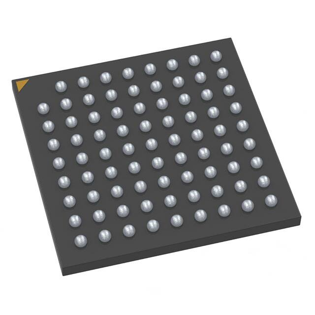
IBGA63 9 y 9
CASE 503AG
Table 1. KEY PERFORMANCE PARAMETERS
Parameter
Typical Value
Optical Format
1/3-inch (6 mm)
Active Pixels
1280 (H) × 960 (V) = 1.2 Mp
Pixel Size
3.75 mm
Color Filter Array
RGB Bayer or Monochrome
Shutter Type
Global Shutter
Input Clock Range
6–50 MHz
Output Pixel Clock (Maximum)
74.25 MHz
Output
Serial
Parallel
HiSPi
12-bit
Frame Rate
Full Resolution
720p
54 fps
60 fps
Responsivity
Monochrome
Color
6.1 V/lux−sec
5.3 V/lux−sec
SNRMAX
38.6 dB
Dynamic Range
64 dB
Supply Voltage
I/O
Digital
Analog
HiSPi
1.8 or 2.8 V
1.8 V
2.8 V
0.4 V
•
•
•
•
•
•
•
•
•
Power Consumption
< 400 mW
Applications
Operating Temperature
–30°C to + 70°C (Ambient)
–30°C to + 80°C (Junction)
Package Options
9 × 9 mm 63-pin iBGA
ILCC48 10 y 10
CASE 847AE
ORDERING INFORMATION
See detailed ordering and shipping information on page 2 of
this data sheet.
Features
• ON Semiconductor’s 3rd Generation Global
Shutter Technology
Superior Low-light Performance
HD Video (720p60)
Video/Single Frame Mode
Flexible Row-skip Modes
On-chip AE and Statistics Engine
Parallel and Serial Output
Support for External LED or Flash
Auto Black Level Calibration
Context Switching
• Scene Processing
• Scanning and Machine Vision
• 720p60 Video Applications
10 × 10 mm 48-pin iLCC
Bare Die
© Semiconductor Components Industries, LLC, 2012
March, 2020 − Rev. 10
1
Publication Order Number:
AR0134CS/D
�AR0134CS
ORDERING INFORMATION
Table 2. ORDERABLE PART NUMBERS
Part Number
Description
Orderable Product Attribute Description
AR0134CSSM25SUEA0−DRBR1
Mono, 25° CRA, iBGA
Dry Pack With No Protective Film MOQ 260
AR0134CSSC00SPD20
Color, 0° CRA, Bare Die
AR0134CSSM00SPD20
Mono, 0° CRA, Bare Die
AR0134CSSC00SUEAH3−GEVB
Color, 0° CRA, Headboard
AR0134CSSC00SPCA0−DPBR
Color, 0° CRA, iLCC
Dry Pack With Protective Film
AR0134CSSC00SPCA0−DRBR
Color, 0° CRA, iLCC
Dry Pack No Protective Film
AR0134CSSC00SUEA0−DPBR
Color, 0° CRA, iBGA
Dry Pack With Protective Film
AR0134CSSC00SUEA0−DRBR
Color, 0° CRA, iBGA
Dry Pack No Protective Film
AR0134CSSM00SPCA0−DPBR
Mono, 0° CRA, iLCC
Dry Pack With Protective Film
AR0134CSSM00SPCA0−DRBR
Mono, 0° CRA, iLCC
Dry Pack No Protective Film
AR0134CSSM00SUEA0−DPBR
Mono, 0° CRA, iBGA
Dry Pack With Protective Film
AR0134CSSM00SUEA0−DRBR
Mono, 0° CRA, iBGA
Dry Pack No Protective Film
AR0134CSSM25SUEA0−DRBR
Mono, 25° CRA, iBGA
Dry Pack No Protective Film
AR0134CSSC00SUEA0−DPBR1
Color, 0° CRA, iBGA
Dry Pack With Protective Film MOQ 260
AR0134CSSM00SUEA0−DPBR1
Mono, 0° CRA, iBGA
Dry Pack With Protective Film MOQ 260
AR0134CSSM00SPCA0−DPBR1
Mono, 0° CRA, iLCC
Dry Pack With Protective Film MOQ 240
AR0134CSSC00SPCA0−TPBR
Color, 0° CRA, iLCC
Tape and Reel With Protective Film
AR0134CSSC00SPCA0−TRBR
Color, 0° CRA, iLCC
Tape and Reel No Protective Film
AR0134CSSC00SUEA0−TPBR
Color, 0° CRA, iBGA
Tape and Reel With Protective Film
AR0134CSSC00SUEA0−TRBR
Color, 0° CRA, iBGA
Tape and Reel No Protective Film
AR0134CSSM00SPCA0−TPBR
Mono, 0° CRA, iLCC
Tape and Reel With Protective Film
AR0134CSSM00SPCA0−TRBR
Mono, 0° CRA, iLCC
Tape and Reel No Protective Film
AR0134CSSM00SUEA0−TPBR
Mono, 0° CRA, iBGA
Tape and Reel With Protective Film
AR0134CSSM00SUEA0−TRBR
Mono, 0° CRA, iBGA
Tape and Reel No Protective Film
AR0134CSSM25SPCA0−TPBR
Mono, 25° CRA, iLCC
Tape and Reel With Protective Film
AR0134CSSM25SUEA0−TPBR
Mono, 25° CRA, iBGA
Tape and Reel With Protective Film
AR0134CSSM25SUEA0−TRBR
Mono, 25° CRA, iBGA
Tape and Reel No Protective Film
AR0134CSSM25SUEA0−DPBR
Mono, 25° CRA, iBGA
Dry Pack With Protective Film
AR0134CSSM25SPD20
Mono, 25° CRA, Bare Die
AR0134CSSM00SPCA0−DPBR2
Mono, 0°. CRA, iLCC
AR0134CSSM00SUEAH3−GEVB
Mono, 0° CRA, Headboard
AR0134CSSM25SUEAH3−GEVB
Mono, 25° CRA, Headboard
Dry Pack with Protective Film MOQ
(HiSPi) output ports. The device may be operated in video
(master) mode or in frame trigger mode.
FRAME_VALID and LINE_VALID signals are output on
dedicated pins, along with a synchronized pixel clock.
A dedicated FLASH pin can be programmed to control
external LED or flash exposure illumination.
The AR0134CS includes additional features to allow
application-specific tuning: windowing, adjustable
auto-exposure control, auto black level correction, on-board
temperature sensor, and row skip and digital binning modes.
The sensor is designed to operate in a wide temperature
range (–30°C to +70°C).
See the ON Semiconductor Device Nomenclature
document (TND310/D) for a full description of the naming
convention used for image sensors. For reference
documentation, including information on evaluation kits,
please visit our web site at www.onsemi.com.
GENERAL DESCRIPTION
The ON Semiconductor AR0134CS can be operated in its
default mode or programmed for frame size, exposure, gain,
and other parameters. The default mode output is
a full-resolution image at 54 frames per second (fps). It
outputs 12-bit raw data, using either the parallel or serial
www.onsemi.com
2
�AR0134CS
FUNCTIONAL OVERVIEW
The AR0134CS is a progressive-scan sensor that
generates a stream of pixel data at a constant frame rate. It
uses an on-chip, phase-locked loop (PLL) that can be
optionally enabled to generate all internal clocks from a
Power
Trigger
Two-wire
Serial
Interface
Active Pixel Sensor
(APS)
Array
single master input clock running between 6 and 50 MHz.
The maximum output pixel rate is 74.25 Mp/s,
corresponding to a clock rate of 74.25 MHz. Figure 1 shows
a block diagram of the sensor.
Temperature
Sensor
OTPM
Timing and Control
(Sequencer)
Memory
Auto Exposure
and Stats Engine
Pixel Data Path
(Signal Processing)
Analog Processing and
A/D Conversion
PLL
External
Clock
Serial
Output
Parallel
Output
Flash
Control Registers
Figure 1. Block Diagram
User interaction with the sensor is through the two-wire
serial bus, which communicates with the array control,
analog signal chain, and digital signal chain. The core of the
sensor is a 1.2 Mp Active-Pixel Sensor array. The
AR0134CS features global shutter technology for accurate
capture of moving images. The exposure of the entire array
is controlled by programming the integration time by
register setting. All rows simultaneously integrate light prior
to readout. Once a row has been read, the data from the
columns is sequenced through an analog signal chain
(providing offset correction and gain), and then through an
analog-to-digital converter (ADC). The output from the
ADC is a 12-bit value for each pixel in the array. The ADC
output passes through a digital processing signal chain
(which provides further data path corrections and applies
digital gain). The pixel data are output at a rate of up to
74.25 Mp/s, in parallel to frame and line synchronization
signals.
•
•
•
•
FEATURES OVERVIEW
The AR0134CS Global Sensor shutter has a wide array of
features to enhance functionality and to increase versatility.
A summary of features follows. Please refer to the
AR0134CS Developer Guide for detailed feature
descriptions, register settings, and tuning guidelines and
recommendations.
• Operating Modes
The AR0134CS works in master (video), trigger (single
frame), or Auto Trigger modes. In master mode, the
sensor generates the integration and readout timing.
In trigger mode, it accepts an external trigger to start
exposure, then generates the exposure and readout
timing. The exposure time is programmed through the
•
•
two-wire serial interface for both modes. Trigger mode
is not compatible with the HiSPi interface.
Window Control
Configurable window size and blanking times allow
a wide range of resolutions and frame rates. Digital
binning and skipping modes are supported, as are
vertical and horizontal mirror operations.
Context Switching
Context switching may be used to rapidly switch
between two sets of register values. Refer to the
AR0134CS Developer Guide for a complete set of
context switchable registers.
Gain
The AR0134CS Global Shutter sensor can be
configured for analog gain of up to 8x, and digital gain
of up to 8x.
Automatic Exposure Control
The integrated automatic exposure control may be used
to ensure optimal settings of exposure and gain are
computed and updated every other frame. Refer to the
AR0134CS Developer Guide for more details.
HiSPi
The AR0134CS Global Shutter image sensor supports
two or three lanes of Streaming-SP or Packetized-SP
protocols of ON Semiconductor’s High-Speed Serial
Pixel Interface.
PLL
An on chip PLL provides reference clock flexibility and
supports spread spectrum sources for improved EMI
performance.
www.onsemi.com
3
�AR0134CS
• Reset
•
•
•
•
•
Pixel Array Structure
The AR0134CS pixel array is configured as 1412 columns
by 1028 rows, (see Figure 2). The dark pixels are optically
black and are used internally to monitor black level. Of the
right 108 columns, 64 are dark pixels used for row noise
correction. Of the top 24 rows of pixels, 12 of the dark rows
are used for black level correction. There are 1296 columns
by 976 rows of optically active pixels. While the sensor’s
format is 1280 × 960, the additional active columns and
active rows are included for use when horizontal or vertical
mirrored readout is enabled, to allow readout to start on the
same pixel. The pixel adjustment is always performed for
monochrome or color versions. The active area is
surrounded with optically transparent dummy pixels to
improve image uniformity within the active area. Not all
dummy pixels or barrier pixels can be read out.
1412
1028
•
PIXEL DATA FORMAT
The AR0134CS may be reset by a register write, or by
a dedicated input pin.
Output Enable
The AR0134CS output pins may be tri-stated using
a dedicated output enable pin.
Temperature Sensor
The temperature sensor is only guaranteed to be
functional when the AR0134CS is initially powered-up
or is reset at temperatures at or above 0°C.
Black Level Correction
Row Noise Correction
Column Correction
Test Patterns
Several test patterns may be enabled for debug
purposes. These include a solid color, color bar, fade to
grey, and a walking 1s test pattern.
2 Light Dummy +
4 Barrier +
24 Dark +
4 Barrier +
6 Dark Dummy
2 Light Dummy +
4 Barrier +
100 Dark +
4 Barrier
1296 × 976 (1288 × 968 Active)
4.86 × 3.66 mm2 (4.83 × 3.63 mm2)
2 Light Dummy +
4 Barrier +
6 Dark Dummy
2 Light Dummy +
4 Barrier
Dark Pixel
Light Dummy
Pixel
Barrier Pixel
Figure 2. Pixel Array Description
www.onsemi.com
4
Active Pixel
�AR0134CS
…
Column Readout Direction
Row Readout Direction
Active Pixel (0, 0)
Array Pixel (110, 40)
…
R G R G R
G R G
G B G B G
B G B
R G R G R
G R G
G B G B G
B G B
R G R G R
G R G
G B G B G
B G B
Figure 3. Pixel Color Pattern Detail (Top Right Corner)
CONFIGURATION AND PINOUT
The figures and tables below show a typical configuration
for the AR0134CS image sensor and show the package
pinouts.
Default Readout Order
By convention, the sensor core pixel array is shown with
the first addressable (logical) pixel (0,0) in the top right
corner (see Figure 3). This reflects the actual layout of the
array on the die. Also, the physical location of the first pixel
data read out of the sensor in default condition is that of pixel
(110, 40).
www.onsemi.com
5
�1.5 kW2, 3
1.5 kW2
AR0134CS
Master Clock
(6−50 MHz)
Digital
I/O
Power1
Digital
Core
Power1
HiSPi
Power1
PLL
Power1
Analog
Power1
Analog
Power1
VDD_IO
VDD
VDD_SLVS
VDD_PLL
VAA
VAA_PIX
SLVS0_P
SLVS0_N
SLVS1_P
EXTCLK
SLVS1_N
SLVS2_P
SLVS2_N
SDATA
SCLK
From
Controller
SLVS3_P
SLVS3_N
OE_BAR
STANDBY
RESET_BAR
To Controller
7
7
SLVSC_P
SLVSC_N
FLASH
TEST
VDD_IO
VDD
DGND
AGND
Digital
Ground
Analog
Ground
VDD_SLVS
VDD_PLL
VAA
VAA_PIX
Notes:
1. All power supplies must be adequately decoupled.
2. ON Semiconductor recommends a resistor value of 1.5 kW, but a greater value may be used for slower two-wire speed.
3. This pull-up resistor is not required if the controller drives a valid logic level on SCLK at all times.
4. The parallel interface output pads can be left unconnected if the serial output interface is used.
5. ON Semiconductor recommends that 0.1 mF and 10 mF decoupling capacitors for each power supply are mounted as close as possible
to the pad. Actual values and results may vary depending on the layout and design considerations. Refer to the AR0134CS demo headboard schematics for circuit recommendations.
6. ON Semiconductor recommends that analog power planes be placed in a manner such that coupling with the digital power planes is minimized.
7. Although 4 serial lanes are shown, the AR0134CS supports only 2- or 3-lane HiSPi.
Figure 4. Serial 4-lane HiSPi Interface
www.onsemi.com
6
�1.5 kW2, 3
1.5 kW2
AR0134CS
Master Clock
(6−50 MHz)
Digital
I/O
Power1
Digital
Core
Power1
PLL
Power1
Analog
Power1
Analog
Power1
VDD_IO
VDD
VDD_PLL
VAA
VAA_PIX
DOUT[11:0]
EXTCLK
PIXCLK
SDATA
SCLK
From
Controller
LINE_VALID
To Controller
FRAME_VALID
TRIGGER
OE_BAR
STANDBY
FLASH
RESET_BAR
TEST
VDD_IO
VDD
DGND
AGND
Digital
Ground
Analog
Ground
VDD_PLL
VAA
VAA_PIX
Notes:
1. All power supplies must be adequately decoupled.
2. ON Semiconductor recommends a resistor value of 1.5 kW, but a greater value may be used for slower two-wire speed.
3. This pull-up resistor is not required if the controller drives a valid logic level on SCLK at all times.
4. The serial interface output pads can be left unconnected if the parallel output interface is used.
5. ON Semiconductor recommends that 0.1 mF and 10 mF decoupling capacitors for each power supply are mounted as close as possible
to the pad. Actual values and results may vary depending on the layout and design considerations. Refer to the AR0134CS demo headboard schematics for circuit recommendations.
6. ON Semiconductor recommends that analog power planes be placed in a manner such that coupling with the digital power planes is minimized.
Figure 5. Parallel Pixel Data Interface
www.onsemi.com
7
�AR0134CS
1
A
2
3
4
5
6
7
8
SLVS0N
SLVS0P
SLVS1N
SLVS1P
VDD
VDD
STANDBY
B
VDD_PLL
SLVSCN
SLVSCP
SLVS2N
SLVS2P
VDD
VAA
VAA
C
EXTCLK
VDD_SLVS
(SLVS3N)
(SLVS3P)
DGND
VDD
AGND
AGND
D
SADDR
SCLK
SDATA
DGND
DGND
VDD
VAA_PIX
VAA_PIX
E
LINE_
VALID
FRAME_
VALID
PIXCLK
FLASH
DGND
VDD_IO
RESERVED
RESERVED
F
DOUT8
DOUT9
DOUT10
DOUT11
DGND
VDD_IO
TEST
RESERVED
G
DOUT4
DOUT5
DOUT6
DOUT7
DGND
VDD_IO
TRIGGER
OE_BAR
H
DOUT0
DOUT1
DOUT2
DOUT3
DGND
VDD_IO
VDD_IO
RESET_
BAR
Top View
(Ball Down)
Figure 6. 9 y 9 mm 63-ball iBGA Package
Table 3. PIN DESCRIPTIONS − 63-BALL IBGA PACKAGE
Name
iBGA Pin
Type
Description
SLVS0_N
A2
Output
HiSPi serial data, lane 0, differential N
SLVS0_P
A3
Output
HiSPi serial data, lane 0, differential P
SLVS1_N
A4
Output
HiSPi serial data, lane 1, differential N
HiSPi serial data, lane 1, differential P
SLVS1_P
A5
Output
STANDBY
A8
Input
VDD_PLL
B1
Power
PLL power
SLVSC_N
B2
Output
HiSPi serial DDR clock differential N
Standby-mode enable pin (active HIGH)
www.onsemi.com
8
�AR0134CS
Table 3. PIN DESCRIPTIONS − 63-BALL IBGA PACKAGE (continued)
Name
iBGA Pin
Type
Description
SLVSC_P
B3
Output
HiSPi serial DDR clock differential P
SLVS2_N
B4
Output
HiSPi serial data, lane 2, differential N
SLVS2_P
B5
Output
HiSPi serial data, lane 2, differential P
VAA
B7, B8
Power
Analog power
EXTCLK
C1
Input
VDD_SLVS
C2
Power
HiSPi power (May leave unconnected if parallel interface is used)
SLVS3_N
C3
Output
(Unsupported) HiSPi serial data, lane 3, differential N
SLVS3_P
C4
Output
(Unsupported) HiSPi serial data, lane 3, differential P
DGND
C5, D4, D5, E5, F5, G5, H5
Power
Digital GND
VDD
A6, A7, B6, C6, D6
Power
Digital power
AGND
C7, C8
Power
Analog GND
SADDR
D1
Input
Two-Wire Serial address select
SCLK
D2
Input
Two-Wire Serial clock input
SDATA
D3
I/O
VAA_PIX
D7, D8
Power
Pixel power
LINE_VALID
E1
Output
Asserted when DOUT line data is valid
FRAME_VALID
E2
Output
Asserted when DOUT frame data is valid
PIXCLK
E3
Output
Pixel clock out. DOUT is valid on rising edge of this clock
FLASH
E4
Output
Control signal to drive external light sources
VDD_IO
E6, F6, G6, H6, H7
Power
I/O supply power
DOUT8
F1
Output
Parallel pixel data output
DOUT9
F2
Output
Parallel pixel data output
DOUT10
F3
Output
Parallel pixel data output
DOUT11
F4
Output
Parallel pixel data output (MSB)
TEST
F7
Input
DOUT4
G1
Output
Parallel pixel data output
DOUT5
G2
Output
Parallel pixel data output
DOUT6
G3
Output
Parallel pixel data output
DOUT7
G4
Output
Parallel pixel data output
TRIGGER
G7
Input
Exposure synchronization input (Connect to DGND if HiSPi interface
is used)
OE_BAR
G8
Input
Output enable (active LOW)
DOUT0
H1
Output
Parallel pixel data output (LSB)
DOUT1
H2
Output
Parallel pixel data output
DOUT2
H3
Output
Parallel pixel data output
DOUT3
H4
Output
Parallel pixel data output
RESET_BAR
H8
Input
Asynchronous reset (active LOW). All settings are restored to factory
default
Reserved
E7, E8, F8
N/A
Reserved (do not connect)
External input clock
Two-Wire Serial data I/O
Manufacturing test enable pin (connect to DGND)
www.onsemi.com
9
�6
5
4
3
2
1
48
47
46
45
44
43
DGND
EXTCLK
VDD_PLL
DOUT6
DOUT5
DOUT4
DOUT3
DOUT2
DOUT1
DOUT0
DGND
NC
AR0134CS
13
PIXCLK
VAA
36
14
VDD
AGND
35
15
SCLK
VAA
34
16
SDATA
Reserved
33
17
RESET_BAR
Reserved
32
18
VDD_IO
Reserved
31
DGND
37
30
VAA_PIX
LINE_VALID
VDD_IO
29
12
FRAME_VALID
38
28
VAA_PIX
TRIGGER
DOUT11
27
11
FLASH
39
26
AGND
TEST
DOUT10
25
10
SADDR
40
24
VAA
OE_BAR
DOUT9
23
9
STANDBY
41
22
NC
NC
DOUT8
21
8
NC
42
20
NC
VDD
DOUT7
19
7
Figure 7. 10 y 10 mm 48-pin iLCC Package, Parallel Output
Table 4. PIN DESCRIPTIONS − 48-PIN ILCC PACKAGE, PARALLEL
Pin Number
Name
Type
1
DOUT4
Output
Parallel pixel data output
2
DOUT5
Output
Parallel pixel data output
3
DOUT6
Output
Parallel pixel data output
4
VDD_PLL
Power
PLL power
5
EXTCLK
Input
Description
External input clock
6
DGND
Power
Digital ground
7
DOUT7
Output
Parallel pixel data output
8
DOUT8
Output
Parallel pixel data output
9
DOUT9
Output
Parallel pixel data output
www.onsemi.com
10
�AR0134CS
Table 4. PIN DESCRIPTIONS − 48-PIN ILCC PACKAGE, PARALLEL (continued)
Pin Number
Name
Type
Description
10
DOUT10
Output
Parallel pixel data output
11
DOUT11
Output
Parallel pixel data output (MSB)
12
VDD_IO
Power
I/O supply power
13
PIXCLK
Output
Pixel clock out. DOUT is valid on rising edge of this clock
14
VDD
Power
Digital power
15
SCLK
Input
16
SDATA
I/O
17
RESET_BAR
Input
18
VDD_IO
Power
I/O supply power
19
VDD
Power
Digital power
20
NC
Two-Wire Serial clock input
Two-Wire Serial data I/O
Asynchronous reset (active LOW). All settings are restored to factory default
No connection
21
NC
22
STANDBY
Input
No connection
Standby-mode enable pin (active HIGH)
23
OE_BAR
Input
Output enable (active LOW)
24
SADDR
Input
Two-Wire Serial address select
25
TEST
Input
Manufacturing test enable pin (connect to DGND)
26
FLASH
Output
Flash output control
27
TRIGGER
Input
28
FRAME_VALID
Output
Exposure synchronization input
Asserted when DOUT frame data is valid
29
LINE_VALID
Output
Asserted when DOUT line data is valid
30
DGND
Power
Digital ground
31
Reserved
N/A
Reserved (do not connect)
32
Reserved
N/A
Reserved (do not connect)
33
Reserved
N/A
Reserved (do not connect)
34
VAA
Power
Analog power
35
AGND
Power
Analog ground
36
VAA
Power
Analog power
37
VAA_PIX
Power
Pixel power
38
VAA_PIX
Power
Pixel power
39
AGND
Power
Analog ground
40
VAA
Power
Analog power
41
NC
No connection
42
NC
No connection
43
NC
No connection
44
DGND
Power
Digital ground
45
DOUT0
Output
Parallel pixel data output (LSB)
46
DOUT1
Output
Parallel pixel data output
47
DOUT2
Output
Parallel pixel data output
48
DOUT3
Output
Parallel pixel data output
www.onsemi.com
11
�AR0134CS
TWO-WIRE SERIAL REGISTER INTERFACE
The two-wire serial interface bus enables read/write
access to control and status registers within the AR0134CS.
The interface protocol uses a master/slave model in which
a master controls one or more slave devices. The sensor acts
as a slave device. The master generates a clock (SCLK) that
is an input to the sensor and is used to synchronize transfers.
Data is transferred between the master and the slave on
a bidirectional signal (SDATA). SDATA is pulled up to
VDD_IO off-chip by a 1.5 kW resistor. Either the slave or
master device can drive SDATA LOW − the interface protocol
determines which device is allowed to drive SDATA at any
given time.
The protocols described in the two-wire serial interface
specification allow the slave device to drive SCLK LOW; the
AR0134CS uses SCLK as an input only and therefore never
drives it LOW.
The default slave addresses used by the AR0134CS are 0x20
(write address) and 0x21 (read address) in accordance with
the specification. Alternate slave addresses of 0x30 (write
address) and 0x31 (read address) can be selected by enabling
and asserting the SADDR input.
An alternate slave address can also be programmed
through R0x31FC.
Message Byte
Message bytes are used for sending register addresses and
register write data to the slave device and for retrieving
register read data.
Acknowledge Bit
Each 8-bit data transfer is followed by an acknowledge bit
or a no-acknowledge bit in the SCLK clock period following
the data transfer. The transmitter (which is the master when
writing, or the slave when reading) releases SDATA.
The receiver indicates an acknowledge bit by driving SDATA
LOW. As for data transfers, SDATA can change when SCLK
is LOW and must be stable while SCLK is HIGH.
Protocol
Data transfers on the two-wire serial interface bus are
performed by a sequence of low-level protocol elements:
1. a (repeated) start condition
2. a slave address/data direction byte
3. an (a no) acknowledge bit
4. a message byte
5. a stop condition
No-Acknowledge Bit
The no-acknowledge bit is generated when the receiver
does not drive SDATA LOW during the SCLK clock period
following a data transfer. A no-acknowledge bit is used to
terminate a read sequence.
Typical Sequence
The bus is idle when both SCLK and SDATA are HIGH.
Control of the bus is initiated with a start condition, and the
bus is released with a stop condition. Only the master can
generate the start and stop conditions.
A typical READ or WRITE sequence begins by the
master generating a start condition on the bus. After the start
condition, the master sends the 8-bit slave address/data
direction byte. The last bit indicates whether the request is
for a read or a write, where a “0” indicates a write and a “1”
indicates a read. If the address matches the address of the
slave device, the slave device acknowledges receipt of the
address by generating an acknowledge bit on the bus.
If the request was a WRITE, the master then transfers the
16-bit register address to which the WRITE should take
place. This transfer takes place as two 8-bit sequences and
the slave sends an acknowledge bit after each sequence to
indicate that the byte has been received. The master then
transfers the data as an 8-bit sequence; the slave sends an
acknowledge bit at the end of the sequence. The master stops
writing by generating a (re)start or stop condition.
If the request was a READ, the master sends the 8-bit write
slave address/data direction byte and 16-bit register address,
the same way as with a WRITE request. The master then
generates a (re)start condition and the 8-bit read slave
address/data direction byte, and clocks out the register data,
eight bits at a time. The master generates an acknowledge bit
after each 8-bit transfer. The slave’s internal register address
is automatically incremented after every 8 bits are
transferred. The data transfer is stopped when the master
sends a no-acknowledge bit.
Start Condition
A start condition is defined as a HIGH-to-LOW transition
on SDATA while SCLK is HIGH. At the end of a transfer, the
master can generate a start condition without previously
generating a stop condition; this is known as a “repeated
start” or “restart” condition.
Stop Condition
A stop condition is defined as a LOW-to-HIGH transition
on SDATA while SCLK is HIGH.
Data Transfer
Data is transferred serially, 8 bits at a time, with the MSB
transmitted first. Each byte of data is followed by an
acknowledge bit or a no-acknowledge bit. This data transfer
mechanism is used for the slave address/data direction byte
and for message bytes.
One data bit is transferred during each SCLK clock period.
SDATA can change when SCLK is LOW and must be stable
while SCLK is HIGH.
Slave Address/Data Direction Byte
Bits [7:1] of this byte represent the device slave address
and bit [0] indicates the data transfer direction. A “0” in
bit [0] indicates a WRITE, and a “1” indicates a READ.
www.onsemi.com
12
�AR0134CS
Single READ from Random Location
register data. The master terminates the READ by
generating a no-acknowledge bit followed by a stop
condition. Figure 8 shows how the internal register address
maintained by the AR0134CS is loaded and incremented as
the sequence proceeds.
This sequence (Figure 8) starts with a dummy WRITE to
the 16-bit address that is to be used for the READ. The
master terminates the WRITE by generating a restart
condition. The master then sends the 8-bit read slave
address/data direction byte and clocks out one byte of
Previous Reg Address, N
S
Slave Address
0 A
S = Start Condition
P = Stop Condition
Sr = Restart Condition
A = Acknowledge
A = No-acknowledge
Reg
Address[15:8]
Reg Address, M
Reg
Address[7:0]
A
A Sr
Slave Address
1 A
M+1
Read Data
A
P
Slave to Master
Master to Slave
Figure 8. Single READ from Random Location
Single READ from Current Location
The master terminates the READ by generating
a no-acknowledge bit followed by a stop condition.
The figure shows two independent READ sequences.
This sequence (Figure 9) performs a read using the
current value of the AR0134CS internal register address.
Previous Reg Address, N
S
Slave Address
1 A
Reg Address, N+1
Read Data
A P
S
Slave Address
N+2
1 A
Read Data
A P
Figure 9. Single READ from Current Location
Sequential READ, Start from Random Location
has been transferred, the master generates an acknowledge
bit and continues to perform byte READs until “L” bytes
have been read.
This sequence (Figure 10) starts in the same way as the
single READ from random location (Figure 8). Instead of
generating a no-acknowledge bit after the first byte of data
Previous Reg Address, N
S
Slave Address
0 A Reg Address[15:8]
M+1
Read Data
A Reg Address[7:0]
M+2
A
Read Data
Reg Address, M
M+3
A Sr
Slave Address
M+L−2
A
Read Data
1 A
M+L−1
A
Read Data
Figure 10. Sequential READ, Start from Random Location
www.onsemi.com
13
M+1
Read Data
M+L
A P
A
�AR0134CS
Sequential READ, Start from Current Location
has been transferred, the master generates an acknowledge
bit and continues to perform byte READs until “L” bytes
have been read.
This sequence (Figure 11) starts in the same way as the
single READ from current location (Figure 9). Instead of
generating a no-acknowledge bit after the first byte of data
Previous Reg Address, N
S Slave Address 1 A
N+1
Read Data
A
N+2
Read Data
A
N+L−1
Read Data
A
N+L
Read Data
A
P
Figure 11. Sequential READ, Start from Current Location
Single WRITE to Random Location
then LOW bytes of the register address that is to be written.
The master follows this with the byte of write data.
The WRITE is terminated by the master generating a stop
condition.
This sequence (Figure 12) begins with the master
generating a start condition. The slave address/data
direction byte signals a WRITE and is followed by the HIGH
Previous Reg Address, N
S
Slave Address
0 A
Reg Address[15:8]
Reg Address, M
A
A
Reg Address[7:0]
M+1
A
A
Write Data
P
Figure 12. Single WRITE to Random Location
Sequential WRITE, Start at Random Location
has been transferred, the master generates an acknowledge
bit and continues to perform byte WRITEs until “L” bytes
have been written. The WRITE is terminated by the master
generating a stop condition.
This sequence (Figure 13) starts in the same way as the
single WRITE to random location (Figure 12). Instead of
generating a no-acknowledge bit after the first byte of data
Previous Reg Address, N
S
Slave Address
0 A
M+1
Write Data
Reg Address[15:8]
A
M+2
A
Write Data
Reg Address, M
Reg Address[7:0]
M+3
A
Write Data
M+L−2
A
Write Data
M+1
A
M+L−1
A
Write Data
M+L
A
A
P
Figure 13. Sequential WRITE, Start at Random Location
ELECTRICAL SPECIFICATIONS
Unless otherwise stated, the following specifications
apply to the following conditions:
VDD = 1.8 V –0.10/+0.15;
VDD_IO = VDD_PLL = VAA = VAA_PIX = 2.8 V ±0.3 V;
VDD_SLVS = 0.4 V –0.1/+0.2;
TA = −30°C to +70°C;
Output Load = 10 pF;
PIXCLK Frequency = 74.25 MHz;
HiSPi off.
Two-Wire Serial Register Interface
The electrical characteristics of the two-wire serial
register interface (SCLK, SDATA) are shown in Figure 14 and
Table 5.
www.onsemi.com
14
�AR0134CS
SDATA
tLOW
tf
tSU;DAT
tr
tf
tHD;STA
tBUF
tr
SCLK
tHD;STA
S
NOTE:
tHD;DAT
tSU;STA
tHIGH
tSU;STO
Sr
P
S
Read sequence: For an 8-bit READ, read waveforms start after WRITE command and register address are issued.
Figure 14. Two-Wire Serial Bus Timing Parameters
Table 5. TWO-WIRE SERIAL BUS CHARACTERISTICS
(fEXTCLK = 27 MHz; VDD = 1.8 V; VDD_IO = 2.8 V; VAA = 2.8 V; VAA_PIX = 2.8 V; VDD_PLL = 2.8 V; VDD_DAC = 2.8 V; TA = 25°C)
Standard Mode
Parameter
SCLK Clock Frequency
Fast-Mode
Symbol
Min
Max
Min
Max
Unit
fSCL
0
100
0
400
kHz
tHD;STA
4.0
−
0.6
−
ms
tLOW
4.7
−
1.3
−
ms
Hold Time (Repeated) START
Condition
After This Period, the First Clock
Pulse is Generated
LOW Period of the SCLK Clock
HIGH Period of the SCLK Clock
tHIGH
4.0
−
0.6
−
ms
Set-up Time for a Repeated
START Condition
tSU;STA
4.7
−
0.6
−
ms
Data Hold Time
tHD;DAT
0 (Note 4)
3.45 (Note 5)
0 (Note 6)
0.9 (Note 5)
ms
Data Set-up Time
tSU;DAT
250
−
100 (Note 6)
−
ns
Rise Time of both SDATA and
SCLK Signals
tr
−
1000
20 + 0.1Cb
(Note 7)
300
ns
Fall Time of both SDATA and SCLK
Signals
tf
−
300
20 + 0.1Cb
(Note 7)
300
ns
Set-up Time for STOP Condition
tSU;STO
4.0
−
0.6
−
ms
Bus Free Time between a STOP
and START Condition
tBUF
4.7
−
1.3
−
ms
Capacitive Load for each Bus Line
Cb
−
400
−
400
pF
Serial Interface Input Pin Capacitance
CIN_SI
−
3.3
−
3.3
pF
CLOAD_SD
−
30
−
30
pF
RSD
1.5
4.7
1.5
4.7
kW
SDATA Max Load Capacitance
SDATA Pull-up Resistor
This table is based on I2C standard (v2.1 January 2000). Philips Semiconductor.
Two-wire control is I2C-compatible.
All values referred to VIHmin = 0.9 VDD_IO and VILmax = 0.1 VDD_IO levels. Sensor EXCLK = 27 MHz.
A device must internally provide a hold time of at least 300 ns for the SDATA signal to bridge the undefined region of the falling edge of SCLK.
The maximum tHD;DAT has only to be met if the device does not stretch the LOW period (tLOW) of the SCLK signal.
A Fast-mode I2C-bus device can be used in a Standard-mode I2C-bus system, but the requirement tSU;DAT 250 ns must then be met. This
will automatically be the case if the device does not stretch the LOW period of the SCLK signal. If such a device does stretch the LOW period
of the SCLK signal, it must output the next data bit to the SDATA line tr max + tSU;DAT = 1000 + 250 = 1250 ns (according to the Standard-mode
I2C-bus specification) before the SCLK line is released.
7. Cb = total capacitance of one bus line in pF.
1.
2.
3.
4.
5.
6.
www.onsemi.com
15
�AR0134CS
I/O Timing
edge of PIXCLK. The launch edge of PIXCLK can be
configured in register R0x3028. See Figure 15 and Table 6
for I/O timing (AC) characteristics.
By default, the AR0134CS launches pixel data, FV and
LV with the falling edge of PIXCLK. The expectation is that
the user captures DOUT[11:0], FV and LV using the rising
tR
tF
90%
tRP
tFP
90%
10%
90%
10%
10%
90%
10%
tEXTCLK
EXTCLK
PIXCLK
tPD
Data[11:0]
Pxl_0
Pxl_1
Pxl_2
Pxl_n
tPFL
tPLL
tPLH
tPFH
LINE_VALID/
FRAME_VALID
FRAME_VALID Leads LINE_VALID
by 6 PIXCLKs
FRAME_VALID Trails LINE_VALID
by 6 PIXCLKs
Figure 15. I/O Timing Diagram
Table 6. I/O TIMING CHARACTERISTICS, PARALLEL OUTPUT (1.8 V VDD_IO) (Note 8)
Symbol
Definition
Condition
Min
Typ
Max
Unit
fEXTCLK
Input Clock Frequency
6
−
50
MHz
tEXTCLK
Input Clock Period
20
−
166
ns
tR
Input Clock Rise Time
PLL Enabled
−
3
−
ns
tF
Input Clock Fall Time
PLL Enabled
−
3
−
ns
−
−
600
ns
tJITTER
Input Clock Jitter
tcp
EXTCLK to PIXCLK
Propagation Delay
Nominal Voltages, PLL Disabled,
PIXCLK Slew Rate = 4
5.7
−
14.3
ns
tRP
PIXCLK Rise Time
PCLK Slew Rate = 6
1.3
−
4.0
ns
tFP
PIXCLK Fall Time
PCLK Slew Rate = 6
1.3
−
3.9
ns
40
50
60
%
PIXCLK Duty Cycle
fPIXCLK
PIXCLK Frequency
PIXCLK Slew Rate = 6, Data Slew Rate = 7
6
−
74.25
MHz
tPD
PIXCLK to Data Valid
PIXCLK Slew Rate = 6, Data Slew Rate = 7
−2.5
−
2
ns
tPFH
PIXCLK to FV HIGH
PIXCLK Slew Rate = 6, Data Slew Rate = 7
−2.5
−
2
ns
tPLH
PIXCLK to LV HIGH
PIXCLK Slew Rate = 6, Data Slew Rate = 7
−3
−
1.5
ns
tPFL
PIXCLK to FV LOW
PIXCLK Slew Rate = 6, Data Slew Rate = 7
−2.5
−
2
ns
tPLL
PIXCLK to LV LOW
PIXCLK Slew Rate = 6, Data Slew Rate = 7
−3
−
1.5
ns
CIN
Input Pin Capacitance
−
2.5
−
pF
8. Minimum and maximum values are taken at 70°C, 1.7 V and −30°C, 1.95 V. All values are taken at the 50% transition point. The loading used
is 10 pF.
9. Jitter from PIXCLK is already taken into account in the data for all of the output parameters.
Table 7. I/O TIMING CHARACTERISTICS, PARALLEL OUTPUT (2.8 V VDD_IO) (Note 10)
Symbol
Definition
Condition
Min
Typ
Max
Unit
fEXTCLK
Input Clock Frequency
6
−
50
MHz
tEXTCLK
Input Clock Period
20
−
166
ns
tR
Input Clock Rise Time
PLL Enabled
−
3
−
ns
tF
Input Clock Fall Time
PLL Enabled
−
3
−
ns
www.onsemi.com
16
�AR0134CS
Table 7. I/O TIMING CHARACTERISTICS, PARALLEL OUTPUT (2.8 V VDD_IO) (Note 10) (continued)
Symbol
Definition
tJITTER
Input Clock Jitter
Condition
Min
Typ
Max
Unit
−
−
600
ns
tcp
EXTCLK to PIXCLK
Propagation Delay
Nominal Voltages, PLL Disabled,
PIXCLK Slew Rate = 4
5.3
−
13.4
ns
tRP
PIXCLK Rise Time
PCLK Slew Rate = 6
1.3
−
4.0
ns
tFP
PIXCLK Fall Time
PCLK slew rate = 6
1.3
−
3.9
ns
PIXCLK Duty Cycle
40
50
60
%
PIXCLK Frequency
PIXCLK Slew Rate = 6, Data Slew Rate = 7
6
−
74.25
MHz
tPD
PIXCLK to Data Valid
PIXCLK Slew Rate = 6, Data Slew Rate = 7
−2.5
−
2
ns
tPFH
PIXCLK to FV HIGH
PIXCLK Slew Rate = 6, Data Slew Rate = 7
−2.5
−
2
ns
tPLH
PIXCLK to LV HIGH
PIXCLK Slew Rate = 6, Data Slew Rate = 7
−2.5
−
2
ns
tPFL
PIXCLK to FV LOW
PIXCLK Slew Rate = 6, Data Slew Rate = 7
−2.5
−
2
ns
tPLL
PIXCLK to LV LOW
PIXCLK Slew Rate = 6, Data Slew Rate = 7
−2.5
−
2
ns
CIN
Input Pin Capacitance
−
2.5
−
pF
fPIXCLK
10. Minimum and maximum values are taken at 70°C, 2.5 V and −30°C, 3.1 V. All values are taken at the 50% transition point. The loading used
is 10 pF.
11. Jitter from PIXCLK is already taken into account in the data for all of the output parameters.
Table 8. I/O RISE SLEW RATE (2.8 V VDD_IO) (Note 12)
Parallel Slew (R0x306E[15:13])
Condition
Min
Typ
Max
Unit
7
Default
1.50
2.50
3.90
V/ns
6
Default
0.98
1.62
2.52
V/ns
5
Default
0.71
1.12
1.79
V/ns
4
Default
0.52
0.82
1.26
V/ns
3
Default
0.37
0.58
0.88
V/ns
2
Default
0.26
0.40
0.61
V/ns
1
Default
0.17
0.27
0.40
V/ns
0
Default
0.10
0.16
0.23
V/ns
12. Minimum and maximum values are taken at 70°C, 2.5 V and −30°C, 3.1 V. The loading used is 10 pF.
Table 9. I/O FALL SLEW RATE (2.8 V VDD_IO) (Note 13)
Parallel Slew (R0x306E[15:13])
Condition
Min
Typ
Max
Unit
7
Default
1.40
2.30
3.50
V/ns
6
Default
0.97
1.61
2.48
V/ns
5
Default
0.73
1.21
1.86
V/ns
4
Default
0.54
0.88
1.36
V/ns
3
Default
0.39
0.63
0.88
V/ns
2
Default
0.27
0.43
0.66
V/ns
1
Default
0.18
0.29
0.44
V/ns
0
Default
0.11
0.17
0.25
V/ns
13. Minimum and maximum values are taken at 70°C, 2.5 V and −30°C, 3.1 V. The loading used is 10 pF.
Table 10. I/O RISE SLEW RATE (1.8 V VDD_IO) (Note 14)
Parallel Slew (R0x306E[15:13])
Condition
Min
Typ
Max
Unit
7
Default
0.57
0.91
1.55
V/ns
6
Default
0.39
0.61
1.02
V/ns
5
Default
0.29
0.46
0.75
V/ns
www.onsemi.com
17
�AR0134CS
Table 10. I/O RISE SLEW RATE (1.8 V VDD_IO) (Note 14) (continued)
Parallel Slew (R0x306E[15:13])
Condition
Min
Typ
Max
Unit
4
Default
0.22
0.34
0.54
V/ns
3
Default
0.16
0.24
0.39
V/ns
2
Default
0.12
0.17
0.27
V/ns
1
Default
0.08
0.11
0.18
V/ns
0
Default
0.05
0.07
0.10
V/ns
14. Minimum and maximum values are taken at 70°C, 1.7 V and −30°C, 1.95 V. The loading used is 10 pF.
Table 11. I/O FALL SLEW RATE (1.8 V VDD_IO) (Note 15)
Parallel Slew (R0x306E[15:13])
Condition
Min
Typ
Max
Unit
7
Default
0.57
0.92
1.55
V/ns
6
Default
0.40
0.64
1.08
V/ns
5
Default
0.31
0.50
0.82
V/ns
4
Default
0.24
0.38
0.61
V/ns
3
Default
0.18
0.27
0.44
V/ns
2
Default
0.13
0.19
0.31
V/ns
1
Default
0.09
0.13
0.20
V/ns
0
Default
0.05
0.08
0.12
V/ns
15. Minimum and maximum values are taken at 70°C, 1.7 V and −30°C, 1.95 V. The loading used is 10 pF.
DC Electrical Characteristics
The DC electrical characteristics are shown in Table 12,
Table 13, Table 14, and Table 15.
Table 12. DC ELECTRICAL CHARACTERISTICS
Symbol
VDD
VDD_IO
VAA
Definition
Condition
Min
Typ
Max
Unit
1.7
1.8
1.95
V
1.7/2.5
1.8/2.8
1.9/3.1
V
Core Digital Voltage
I/O Digital Voltage
Analog Voltage
2.5
2.8
3.1
V
VAA_PIX
Pixel Supply Voltage
2.5
2.8
3.1
V
VDD_PLL
PLL Supply Voltage
2.5
2.8
3.1
V
VDD_SLVS
0.3
0.4
0.6
V
VIH
Input HIGH Voltage
VDD_IO × 0.7
–
–
V
VIL
Input LOW Voltage
–
–
VDD_IO × 0.3
V
IIN
Input Leakage Current
20
–
–
mA
VOH
Output HIGH Voltage
VDD_IO – 0.3
–
–
V
VOL
Output LOW Voltage
VDD_IO = 2.8 V
–
–
0.4
V
IOH
Output HIGH Current
At Specified VOH
–22
–
–
mA
IOL
Output LOW Current
At Specified VOL
–
–
22
mA
CAUTION:
HiSPi Supply Voltage
No Pull-up Resistor;
VIN = VDD_IO or DGND
Stresses greater than those listed in Table 13 may cause permanent damage to the device. This is a stress rating only, and
functional operation of the device at these or any other conditions above those indicated in the operational sections of this
specification is not implied.
www.onsemi.com
18
�AR0134CS
Table 13. ABSOLUTE MAXIMUM RATINGS
Symbol
Parameter
VSUPPLY
Power Supply Voltage (All Supplies)
ISUPPLY
Total Power Supply Current
Minimum
Maximum
Unit
–0.3
4.5
V
–
200
mA
IGND
Total Ground Current
–
200
mA
VIN
DC Input Voltage
–0.3
VDD_IO + 0.3
V
VOUT
DC Output Voltage
–0.3
VDD_IO + 0.3
V
TSTG
Storage Temperature (Note 16)
–40
+85
°C
Stresses exceeding those listed in the Maximum Ratings table may damage the device. If any of these limits are exceeded, device functionality
should not be assumed, damage may occur and reliability may be affected.
16. Exposure to absolute maximum rating conditions for extended periods may affect reliability.
Table 14. OPERATING CURRENT CONSUMPTION FOR PARALLEL OUTPUT
(VAA = VAA_PIX = VDD_IO = VDD_PLL = 2.8 V; VDD = 1.8 V; PLL Enabled and PIXCLK = 74.25 MHz; TA = 25°C; CLOAD = 10 pF)
Condition
Min
Typ
Max
Unit
Digital Operating Current
Parallel, Streaming, Full Resolution 54 fps
−
46
60
mA
I/O Digital Operating Current
Parallel, Streaming, Full Resolution 54 fps
−
52
–
mA
Analog Operating Current
Parallel, Streaming, Full Resolution 54 fps
−
46
55
mA
IAA_PIX
Pixel Supply Current
Parallel, Streaming, Full Resolution 54 fps
−
7
9
mA
IDD_PLL
PLL Supply Current
Parallel, Streaming, Full Resolution 54 fps
−
8
10
mA
Symbol
IDD1
IDD_IO
IAA
Parameter
Table 15. STANDBY CURRENT CONSUMPTION
(Analog − VAA + VAA_PIX + VDD_PLL; Digital − VDD + VDD_IO; TA = 25°C)
Condition
Min
Analog, 2.8 V
Digital, 1.8 V
Hard Standby (Clock On, EXTCLK = 20 MHz)
Soft Standby (Clock Off, Driven Low)
Soft Standby (Clock On, EXTCLK = 20 MHz)
Digital, 1.8 V
Definition
Hard Standby (Clock Off, Driven Low)
Typ
Max
Unit
–
3
15
mA
–
25
80
mA
Analog, 2.8 V
–
12
25
mA
Digital, 1.8 V
–
1.1
1.7
mA
Analog, 2.8 V
–
3
15
mA
Digital, 1.8 V
–
25
80
mA
Analog, 2.8 V
–
12
25
mA
–
1.1
1.7
mA
www.onsemi.com
19
�AR0134CS
HiSPi Electrical Specifications
information. The VDD_SLVS supply in this data sheet
corresponds to VDD_TX in the HiSPi Physical Layer
Specification. Similarly, VDD is equivalent to VDD_HiSPi
as referenced in the specification. The HiSPi transmitter
electrical specifications are listed at 700 MHz.
The ON Semiconductor AR0134CS sensor supports
SLVS mode only, and does not have a DLL for timing
adjustments. Refer to the High-Speed Serial Pixel (HiSPi)
Interface Physical Layer Specification v2.00.00 for
electrical definitions, specifications, and timing
Table 16. INPUT VOLTAGE AND CURRENT (HiSPi POWER SUPPLY 0.4 V)
(Measurement Conditions: Max Freq. 700 MHz)
Symbol
IDD_SLVS
Parameter
Min
Typ
Max
Unit
–
10
15
mA
VCMD
HiSPi Common Mode Voltage (Driving 100 W Load)
VDD_SLVS ×
0.45
VDD_SLVS/2
VDD_SLVS ×
0.55
V
|VOD|
HiSPi Differential Output Voltage (Driving 100 W Load)
VDD_SLVS ×
0.36
VDD_SLVS/2
VDD_SLVS ×
0.64
V
DVCM
Change in VCM between Logic 1 and 0
−
−
25
mV
|VOD|
Change in |VOD| between Logic 1 and 0
−
−
25
mV
VOD Noise Margin
–
−
30
%
|DVCM|
Difference in VCM between any Two Channels
−
−
50
mV
|DVOD|
Difference in VOD between any Two Channels
−
−
100
mV
DVCM_ac
Common-mode AC Voltage (pk) without VCM Cap Termination
−
−
50
mV
DVCM_ac
NM
Supply Current (PWRHiSPi) (Driving 100 W Load)
Common-mode AC Voltage (pk) with VCM Cap Termination
−
−
30
mV
VOD_ac
Max Overshoot Peak |VOD|
−
−
1.3 × |VOD|
V
Vdiff_pkpk
Max Overshoot Vdiff pk-pk
V
Veye
Ro
DRo
−
−
2.6 × |VOD|
1.4 × VOD
−
−
Single-ended Output Impedance
35
50
70
W
Output Impedance Mismatch
−
−
20
%
Eye Height
www.onsemi.com
20
�AR0134CS
VDIFFmax
VDIFFmin
0 V (Diff)
Output Signal
is ‘Cp − Cn’ or
‘Dp − Dn’
Figure 16. Differential Output Voltage for Clock and Data Pairs
Table 17. RISE AND FALL TIMES
(Measurement Conditions: HiSPi Power Supply 0.4 V, Max Freq. 700 MHz)
Parameter
Min
Typ
Max
Unit
Data Rate
280
–
700
Mb/s
TxPRE
Max Setup Time from Transmitter (Note 17)
0.3
–
–
UI
TxPost
Max Hold Time from Transmitter
0.3
–
–
UI
–
Symbol
1/UI
RISE
Rise Time (20% − 80%)
–
0.25 UI
FALL
Fall Time (20% − 80%)
150 ps
0.25 UI
–
45
50
55
%
3.57
ns
PLL_DUTY
Clock Duty
tpw
Bitrate Period (Note 17)
1.43
−
teye
Eye Width (Notes 17, 18)
0.3
−
−
UI
Data Total Jitter (pk pk)@1e−9 (Notes 17, 18)
−
−
0.2
UI
tckjit
Clock Period Jitter (RMS) (Note 18)
−
−
50
ps
tcyjit
Clock Cycle to Cycle Jitter (RMS) (Note 18)
ttotaljit
−
−
100
ps
tchskew
Clock to Data Skew (Notes 17, 18)
−0.1
−
0.1
UI
t|PHYskew|
PHY-to-PHY Skew (Notes 17, 21)
−
−
2.1
UI
tDIFFSKEW
Mean Differential Skew (Note 22)
–100
−
100
ps
17. One UI is defined as the normalized mean time between one edge and the following edge of the clock.
18. Taken from 0 V crossing point.
19. Also defined with a maximum loading capacitance of 10 pF on any pin. The loading capacitance may also need to be less for higher bitrates
so the rise and fall times do not exceed the maximum 0.3 UI.
20. The absolute mean skew between the Clock lane and any Data Lane in the same PHY between any edges.
21. The absolute mean skew between any Clock in one PHY and any Data lane in any other PHY between any edges.
22. Differential skew is defined as the skew between complementary outputs. It is measured as the absolute time between the two
complementary edges at mean VCM point.
www.onsemi.com
21
�AR0134CS
RISE
VDIFF
80%
DATA MASK
20%
TxPre
TxPost
FALL
Max VDIFF
CLOCK MASK
UI/2
VDIFF
UI/2
CLKJITTER
Trigger/Reference
Figure 17. Eye Diagram for Clock and Data Signals
VCMD
tCMPSKEW
tCHSKEW1PHY
Figure 18. Skew within the PHY and Output Channels
www.onsemi.com
22
�AR0134CS
POWER-ON RESET AND STANDBY TIMING
5. If RESET_BAR is in a LOW state, hold
RESET_BAR LOW for at least 1 ms.
If RESET_BAR is in a HIGH state, assert
RESET_BAR for at least 1 ms.
6. Wait 160000 EXTCLKs (for internal initialization
into software standby).
7. Configure PLL, output, and image settings to
desired values.
8. Wait 1 ms for the PLL to lock.
9. Set streaming mode (R0x301a[2] = 1).
Power-Up Sequence
The recommended power-up sequence for the AR0134CS
is shown in Figure 19. The available power supplies
(VDD_IO, VDD, VDD_SLVS, VDD_PLL, VAA, VAA_PIX)
must have the separation specified below.
1. Turn on VDD_PLL power supply.
2. After 0−10 ms, turn on VAA and VAA_PIX power
supply.
3. After 0−10 ms, turn on VDD_IO power supply.
4. After the last power supply is stable, enable
EXTCLK.
VDD_PLL (2.8)
t0
VAA_PIX
VAA (2.8)
t1
VDD_IO (1.8/2.8)
t2
VDD (1.8)
t3
VDD_SLVS (0.4)
EXTCLK
t4
RESET_BAR
t5
tX
Hard
Reset
t6
Internal Initialization
Software
Standby
PLL Clock
Streaming
Figure 19. Power Up
Table 18. POWER-UP SEQUENCE
Symbol
Definition
Min
Typ
Max
Unit
t0
VDD_PLL to VAA/VAA_PIX
0
10
–
ms
t1
VAA/VAA_PIX to VDD_IO
0
10
–
ms
t2
VDD_IO to VDD
0
10
–
ms
t3
VDD to VDD_SLVS
0
10
–
ms
tX
Xtal Settle Time
–
30 (Note 23)
–
ms
t4
Hard Reset
1 (Note 24)
–
–
ms
t5
Internal Initialization
160000
–
–
EXTCLKs
t6
PLL Lock Time
1
–
–
ms
23. Xtal settling time is component-dependent, usually taking about 10–100 ms.
24. Hard reset time is the minimum time required after power rails are settled. In a circuit where hard reset is held down by RC circuit, then the
RC time must include the all power rail settle time and Xtal settle time.
25. It is critical that VDD_PLL is not powered up after the other power supplies. It must be powered before or at least at the same time as the
others. If the case happens that VDD_PLL is powered after other supplies then the sensor may have functionality issues and will experience
high current draw on this supply.
www.onsemi.com
23
�AR0134CS
Power-Down Sequence
The recommended power-down sequence for the
AR0134CS is shown in Figure 20. The available power
supplies (VDD_IO, VDD, VDD_SLVS, VDD_PLL, VAA,
VAA_PIX) must have the separation specified below.
1. Disable streaming if output is active by setting
standby R0x301a[2] = 0.
2. The soft standby state is reached after the current
row or frame, depending on configuration, has
ended.
3. Turn off VDD_SLVS.
4. Turn off VDD.
5. Turn off VDD_IO.
6. Turn off VAA/VAA_PIX.
7. Turn off VDD_PLL.
VDD_SLVS (0.4)
t0
VDD (1.8)
t1
VDD_IO (1.8/2.8)
t2
VAA_PIX
VAA (2.8)
t3
VDD_PLL (2.8)
EXTCLK
t4
Power Down until Next
Power Up Cycle
Figure 20. Power Down
Table 19. POWER-DOWN SEQUENCE
Symbol
Parameter
Min
Typ
Max
Unit
t0
VDD_SLVS to VDD
0
–
–
ms
t1
VDD to VDD_IO
0
–
–
ms
t2
VDD_IO to VAA/VAA_PIX
0
–
–
ms
t3
VAA/VAA_PIX to VDD_PLL
0
–
–
ms
t4
PwrDn until Next PwrUp Time
100
–
–
ms
26. t4 is required between power down and next power up time; all decoupling caps from regulators must be completely discharged.
www.onsemi.com
24
�AR0134CS
Standby Sequence
the last valid register write prior to entering standby as well
as the first valid write upon exiting standby. Also shown is
timing if the EXTCLK is to be disabled during standby.
Figure 21 and Figure 22 show timing diagrams for
entering and exiting standby. Delays are shown indicating
FV
EXTCLK
50 EXTCLKs
SDATA Register Writes Valid
Register Writes Not Valid
750 EXTCLKs
STANDBY
Figure 21. Enter Standby Timing
28 Rows + CIT
FV
EXTCLK
SDATA
Register Writes Not Valid
Register Writes Valid
10 EXTCLKs
STANDBY
1 ms
TRIGGER
Figure 22. Exit Standby Timing
www.onsemi.com
25
�AR0134CS
80
70
Quantum Efficiency (%)
60
50
40
30
20
10
0
350
400
450
500
550
600
700
650
800
750
850
900
950
1000 1050
1100
Wavelength (nm)
Figure 23. Quantum Efficiency − Monochrome Sensor (Typical)
70
Red
Green
Blue
60
Quantum Efficiency (%)
50
40
30
20
10
0
350
400
450
500
550
600
650
700
750
800
850
900
Wavelength (nm)
Figure 24. Quantum Efficiency − Color Sensor (Typical)
www.onsemi.com
26
950
1000
1050
�AR0134CS
CRA vs. Image Height Plot
CRA
(%)
(deg)
(mm)
0
0
0
5
0.150
1.35
30
10
0.300
2.70
28
15
0.450
4.04
26
20
0.600
5.39
24
25
0.750
6.73
30
0.900
8.06
35
1.050
9.39
16
40
1.200
10.71
14
45
1.350
12.02
12
50
1.500
13.33
10
55
1.650
14.62
8
60
1.800
15.90
65
1.950
17.16
70
2.100
18.41
75
2.250
19.64
80
2.400
20.85
85
2.550
22.05
90
2.700
23.22
95
2.850
24.38
100
3.000
25.51
AR0134CS CRA Characteristic
Chief Ray Angle (Degrees)
Image Height
22
20
18
6
4
2
0
0
10
20
30
40
50
60
70
80
Image Height (%)
Figure 25. Chief Ray Angle − 255 Mono
www.onsemi.com
27
90
100
110
�MECHANICAL CASE OUTLINE
PACKAGE DIMENSIONS
IBGA63 9x9
CASE 503AG
ISSUE C
DATE 21 FEB 2020
GENERIC
MARKING DIAGRAM*
XXXX = Specific Device Code
Y
= Year
ZZZ = Assembly Lot Code
*This information is generic. Please refer to
device data sheet for actual part marking.
Pb−Free indicator, “G” or microdot “G”, may
or may not be present. Some products may
not follow the Generic Marking.
DOCUMENT NUMBER:
DESCRIPTION:
98AON93394F
IBGA63 9x9
Electronic versions are uncontrolled except when accessed directly from the Document Repository.
Printed versions are uncontrolled except when stamped “CONTROLLED COPY” in red.
PAGE 1 OF 1
ON Semiconductor and
are trademarks of Semiconductor Components Industries, LLC dba ON Semiconductor or its subsidiaries in the United States and/or other countries.
ON Semiconductor reserves the right to make changes without further notice to any products herein. ON Semiconductor makes no warranty, representation or guarantee regarding
the suitability of its products for any particular purpose, nor does ON Semiconductor assume any liability arising out of the application or use of any product or circuit, and specifically
disclaims any and all liability, including without limitation special, consequential or incidental damages. ON Semiconductor does not convey any license under its patent rights nor the
rights of others.
© Semiconductor Components Industries, LLC, 2018
www.onsemi.com
�MECHANICAL CASE OUTLINE
PACKAGE DIMENSIONS
ILCC48 10x10
CASE 847AE
ISSUE O
DOCUMENT NUMBER:
98AON93696F
DESCRIPTION:
ILCC48 10X10
DATE 30 DEC 2014
Electronic versions are uncontrolled except when accessed directly from the Document Repository.
Printed versions are uncontrolled except when stamped “CONTROLLED COPY” in red.
PAGE 1 OF 1
ON Semiconductor and
are trademarks of Semiconductor Components Industries, LLC dba ON Semiconductor or its subsidiaries in the United States and/or other countries.
ON Semiconductor reserves the right to make changes without further notice to any products herein. ON Semiconductor makes no warranty, representation or guarantee regarding
the suitability of its products for any particular purpose, nor does ON Semiconductor assume any liability arising out of the application or use of any product or circuit, and specifically
disclaims any and all liability, including without limitation special, consequential or incidental damages. ON Semiconductor does not convey any license under its patent rights nor the
rights of others.
© Semiconductor Components Industries, LLC, 2019
www.onsemi.com
�onsemi,
, and other names, marks, and brands are registered and/or common law trademarks of Semiconductor Components Industries, LLC dba “onsemi” or its affiliates
and/or subsidiaries in the United States and/or other countries. onsemi owns the rights to a number of patents, trademarks, copyrights, trade secrets, and other intellectual property.
A listing of onsemi’s product/patent coverage may be accessed at www.onsemi.com/site/pdf/Patent−Marking.pdf. onsemi reserves the right to make changes at any time to any
products or information herein, without notice. The information herein is provided “as−is” and onsemi makes no warranty, representation or guarantee regarding the accuracy of the
information, product features, availability, functionality, or suitability of its products for any particular purpose, nor does onsemi assume any liability arising out of the application or use
of any product or circuit, and specifically disclaims any and all liability, including without limitation special, consequential or incidental damages. Buyer is responsible for its products
and applications using onsemi products, including compliance with all laws, regulations and safety requirements or standards, regardless of any support or applications information
provided by onsemi. “Typical” parameters which may be provided in onsemi data sheets and/or specifications can and do vary in different applications and actual performance may
vary over time. All operating parameters, including “Typicals” must be validated for each customer application by customer’s technical experts. onsemi does not convey any license
under any of its intellectual property rights nor the rights of others. onsemi products are not designed, intended, or authorized for use as a critical component in life support systems
or any FDA Class 3 medical devices or medical devices with a same or similar classification in a foreign jurisdiction or any devices intended for implantation in the human body. Should
Buyer purchase or use onsemi products for any such unintended or unauthorized application, Buyer shall indemnify and hold onsemi and its officers, employees, subsidiaries, affiliates,
and distributors harmless against all claims, costs, damages, and expenses, and reasonable attorney fees arising out of, directly or indirectly, any claim of personal injury or death
associated with such unintended or unauthorized use, even if such claim alleges that onsemi was negligent regarding the design or manufacture of the part. onsemi is an Equal
Opportunity/Affirmative Action Employer. This literature is subject to all applicable copyright laws and is not for resale in any manner.
PUBLICATION ORDERING INFORMATION
LITERATURE FULFILLMENT:
Email Requests to: orderlit@onsemi.com
onsemi Website: www.onsemi.com
◊
TECHNICAL SUPPORT
North American Technical Support:
Voice Mail: 1 800−282−9855 Toll Free USA/Canada
Phone: 011 421 33 790 2910
Europe, Middle East and Africa Technical Support:
Phone: 00421 33 790 2910
For additional information, please contact your local Sales Representative
�


 工商网监
湘ICP备2023018690号
工商网监
湘ICP备2023018690号
