BAS40-06LT1G,
SBAS40-06LT1G
Common Anode Schottky
Barrier Diodes
These Schottky barrier diodes are designed for high speed
switching applications, circuit protection, and voltage clamping.
Extremely low forward voltage reduces conduction loss. Miniature
surface mount package is excellent for hand held and portable
applications where space is limited.
www.onsemi.com
40 VOLTS
SCHOTTKY BARRIER DIODE
Features
• Extremely Fast Switching Speed
• Low Forward Voltage
• S Prefix for Automotive and Other Applications Requiring Unique
•
Site and Control Change Requirements; AEC−Q101 Qualified and
PPAP Capable
These Devices are Pb−Free, Halogen Free/BFR Free and are RoHS
Compliant
Reverse Voltage
Symbol
Value
Unit
VR
40
V
2
CATHODE
Stresses exceeding those listed in the Maximum Ratings table may damage the
device. If any of these limits are exceeded, device functionality should not be
assumed, damage may occur and reliability may be affected.
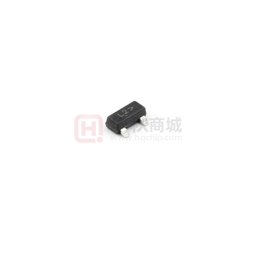
MARKING DIAGRAM
L2 M G
G
THERMAL CHARACTERISTICS
Characteristic
Max
Unit
225
1.8
mW
mW/°C
TJ, Tstg
−55 to +150
°C
Forward Continuous Current
IFM
120
Single Forward Current
tv1s
t v 10 ms
IFSM
Thermal Resistance (Note 1)
Junction−to−Ambient (Note 2)
RqJA
Forward Power Dissipation
@ TA = 25°C
Derate above 25°C
Operating Junction and Storage
Temperature Range
CATHODE
1
ANODE
3
MAXIMUM RATINGS
Rating
SOT−23 (TO−236)
CASE 318
STYLE 12
Symbol
PF
mA
L2 = Specific Device Code
M = Date Code*
G = Pb−Free Package
(Note: Microdot may be in either location)
*Date Code orientation and/or overbar may
vary depending upon manufacturing location.
mA
200
600
ORDERING INFORMATION
°C/W
508
311
1. FR−4 @ minimum pad.
2. FR−4 @ 1.0 x 1.0 in pad.
Package
Shipping†
BAS40−06LT1G
SOT−23
(Pb−Free)
3,000 /
Tape & Reel
SBAS40−06LT1G
SOT−23
(Pb−Free)
3,000 /
Tape & Reel
Device
†For information on tape and reel specifications,
including part orientation and tape sizes, please
refer to our Tape and Reel Packaging Specifications
Brochure, BRD8011/D.
© Semiconductor Components Industries, LLC, 1997
March, 2018 − Rev. 10
1
Publication Order Number:
BAS40−06LT1/D
�BAS40−06LT1G, SBAS40−06LT1G
ELECTRICAL CHARACTERISTICS (TA = 25°C unless otherwise noted)
Characteristic
Symbol
Reverse Breakdown Voltage
(IR = 10 mA)
Min
Max
40
−
−
5.0
−
1.0
−
380
−
500
−
1.0
Unit
V(BR)R
Total Capacitance
(VR = 1.0 V, f = 1.0 MHz)
CT
Reverse Leakage
(VR = 25 V)
IR
Forward Voltage
(IF = 1.0 mAdc)
VF
Forward Voltage
(IF = 10 mAdc)
VF
Forward Voltage
(IF = 40 mAdc)
VF
V
pF
mAdc
mVdc
mVdc
Vdc
Product parametric performance is indicated in the Electrical Characteristics for the listed test conditions, unless otherwise noted. Product
performance may not be indicated by the Electrical Characteristics if operated under different conditions.
TYPICAL CHARACTERISTICS
IR , REVERSE CURRENT (μA)
100
10
150°C
1.0
1�25°C
85°C
25°C
-�40°C
0.1
0
0.1
TA = 150°C
125°C
10
85°C
1.0
0.1
25°C
0.01
0.2
0.3
-�55°C
0.4
0.001
0.5
0.6
0.7
0.8
0
5.0
VF, FORWARD VOLTAGE (VOLTS)
Figure 1. Typical Forward Voltage
10
15
VR, REVERSE VOLTAGE (VOLTS)
3.0
2.5
2.0
1.5
1.0
0.5
0
0
5.0
10
20
Figure 2. Reverse Current versus Reverse
Voltage
3.5
C T, CAPACITANCE (pF)
IF, FORWARD CURRENT (mA)
100
15
20
25
30
VR, REVERSE VOLTAGE (VOLTS)
Figure 3. Typical Capacitance
www.onsemi.com
2
35
40
25
�MECHANICAL CASE OUTLINE
PACKAGE DIMENSIONS
SOT−23 (TO−236)
CASE 318−08
ISSUE AS
DATE 30 JAN 2018
SCALE 4:1
D
0.25
3
E
1
2
T
HE
NOTES:
1. DIMENSIONING AND TOLERANCING PER ASME Y14.5M, 1994.
2. CONTROLLING DIMENSION: MILLIMETERS.
3. MAXIMUM LEAD THICKNESS INCLUDES LEAD FINISH.
MINIMUM LEAD THICKNESS IS THE MINIMUM THICKNESS OF
THE BASE MATERIAL.
4. DIMENSIONS D AND E DO NOT INCLUDE MOLD FLASH,
PROTRUSIONS, OR GATE BURRS.
DIM
A
A1
b
c
D
E
e
L
L1
HE
T
L
3X b
L1
VIEW C
e
TOP VIEW
A
A1
SIDE VIEW
MIN
0.89
0.01
0.37
0.08
2.80
1.20
1.78
0.30
0.35
2.10
0°
MILLIMETERS
NOM
MAX
1.00
1.11
0.06
0.10
0.44
0.50
0.14
0.20
2.90
3.04
1.30
1.40
1.90
2.04
0.43
0.55
0.54
0.69
2.40
2.64
−−−
10 °
MIN
0.035
0.000
0.015
0.003
0.110
0.047
0.070
0.012
0.014
0.083
0°
INCHES
NOM
0.039
0.002
0.017
0.006
0.114
0.051
0.075
0.017
0.021
0.094
−−−
MAX
0.044
0.004
0.020
0.008
0.120
0.055
0.080
0.022
0.027
0.104
10°
c
SEE VIEW C
GENERIC
MARKING DIAGRAM*
END VIEW
RECOMMENDED
SOLDERING FOOTPRINT
XXXMG
G
1
3X
2.90
3X
XXX = Specific Device Code
M = Date Code
G
= Pb−Free Package
(Note: Microdot may be in either location)
0.90
*This information is generic. Please refer to
device data sheet for actual part marking.
Pb−Free indicator, “G” or microdot “ G”,
may or may not be present.
0.95
PITCH
0.80
DIMENSIONS: MILLIMETERS
STYLE 1 THRU 5:
CANCELLED
STYLE 6:
PIN 1. BASE
2. EMITTER
3. COLLECTOR
STYLE 7:
PIN 1. EMITTER
2. BASE
3. COLLECTOR
STYLE 9:
PIN 1. ANODE
2. ANODE
3. CATHODE
STYLE 10:
PIN 1. DRAIN
2. SOURCE
3. GATE
STYLE 11:
STYLE 12:
PIN 1. ANODE
PIN 1. CATHODE
2. CATHODE
2. CATHODE
3. CATHODE−ANODE
3. ANODE
STYLE 15:
PIN 1. GATE
2. CATHODE
3. ANODE
STYLE 16:
PIN 1. ANODE
2. CATHODE
3. CATHODE
STYLE 17:
PIN 1. NO CONNECTION
2. ANODE
3. CATHODE
STYLE 18:
STYLE 19:
STYLE 20:
PIN 1. NO CONNECTION PIN 1. CATHODE
PIN 1. CATHODE
2. CATHODE
2. ANODE
2. ANODE
3. GATE
3. ANODE
3. CATHODE−ANODE
STYLE 21:
PIN 1. GATE
2. SOURCE
3. DRAIN
STYLE 22:
PIN 1. RETURN
2. OUTPUT
3. INPUT
STYLE 23:
PIN 1. ANODE
2. ANODE
3. CATHODE
STYLE 24:
PIN 1. GATE
2. DRAIN
3. SOURCE
STYLE 27:
PIN 1. CATHODE
2. CATHODE
3. CATHODE
STYLE 28:
PIN 1. ANODE
2. ANODE
3. ANODE
DOCUMENT NUMBER:
STATUS:
STYLE 8:
PIN 1. ANODE
2. NO CONNECTION
3. CATHODE
98ASB42226B
ON SEMICONDUCTOR STANDARD
NEW STANDARD:
© Semiconductor Components Industries, LLC, 2002
October, DESCRIPTION:
2002 − Rev. 0
SOT−23 (TO−236)
http://onsemi.com
1
STYLE 13:
PIN 1. SOURCE
2. DRAIN
3. GATE
STYLE 25:
PIN 1. ANODE
2. CATHODE
3. GATE
STYLE 14:
PIN 1. CATHODE
2. GATE
3. ANODE
STYLE 26:
PIN 1. CATHODE
2. ANODE
3. NO CONNECTION
Electronic versions are uncontrolled except when
accessed directly from the Document Repository. Printed
versions are uncontrolled except when stamped
“CONTROLLED COPY” in red.
Case Outline Number:
PAGE 1 OFXXX
2
�DOCUMENT NUMBER:
98ASB42226B
PAGE 2 OF 2
ISSUE
REVISION
DATE
AJ
ADDED STYLE 27. REQ. BY P. LEM.
07 JUL 2004
AK
OBSOLETED −09 VERSION. REQ. BY D. TRUHITTE.
14 SEP 2004
AL
ADDED NOMINAL VALUES AND UPDATED GENERIC MARKING DIAGRAM. REQ.
BY HONG XIAO.
27 MAY 2005
AM
REDREW LEAD SIDE VIEW. REQ BY DARRELL TRUHITTE.
26 AUG 2005
AN
REINTRODUCED LABELS FOR DIMENSION C. REQ. BY D. TRUHITTE.
14 OCT 2005
AP
ADDED THETA DEGREE VALUES TO DIMENSION TABLE. REQ. BY D. TRUHITTE.
17 NOV 2009
AR
MODIFIED DIMENSIONS C AND L. REQ. BY M. YOU.
10 OCT 2016
AS
ADDED STYLE 28. REQ. BY E. ESTILLER.
30 JAN 2018
ON Semiconductor and
are registered trademarks of Semiconductor Components Industries, LLC (SCILLC). SCILLC reserves the right to make changes without further notice
to any products herein. SCILLC makes no warranty, representation or guarantee regarding the suitability of its products for any particular purpose, nor does SCILLC assume any liability
arising out of the application or use of any product or circuit, and specifically disclaims any and all liability, including without limitation special, consequential or incidental damages.
“Typical” parameters which may be provided in SCILLC data sheets and/or specifications can and do vary in different applications and actual performance may vary over time. All
operating parameters, including “Typicals” must be validated for each customer application by customer’s technical experts. SCILLC does not convey any license under its patent rights
nor the rights of others. SCILLC products are not designed, intended, or authorized for use as components in systems intended for surgical implant into the body, or other applications
intended to support or sustain life, or for any other application in which the failure of the SCILLC product could create a situation where personal injury or death may occur. Should
Buyer purchase or use SCILLC products for any such unintended or unauthorized application, Buyer shall indemnify and hold SCILLC and its officers, employees, subsidiaries, affiliates,
and distributors harmless against all claims, costs, damages, and expenses, and reasonable attorney fees arising out of, directly or indirectly, any claim of personal injury or death
associated with such unintended or unauthorized use, even if such claim alleges that SCILLC was negligent regarding the design or manufacture of the part. SCILLC is an Equal
Opportunity/Affirmative Action Employer. This literature is subject to all applicable copyright laws and is not for resale in any manner.
© Semiconductor Components Industries, LLC, 2018
January, 2018 − Rev. AS
Case Outline Number:
318
�ON Semiconductor and
are trademarks of Semiconductor Components Industries, LLC dba ON Semiconductor or its subsidiaries in the United States and/or other countries.
ON Semiconductor owns the rights to a number of patents, trademarks, copyrights, trade secrets, and other intellectual property. A listing of ON Semiconductor’s product/patent
coverage may be accessed at www.onsemi.com/site/pdf/Patent−Marking.pdf. ON Semiconductor reserves the right to make changes without further notice to any products herein.
ON Semiconductor makes no warranty, representation or guarantee regarding the suitability of its products for any particular purpose, nor does ON Semiconductor assume any liability
arising out of the application or use of any product or circuit, and specifically disclaims any and all liability, including without limitation special, consequential or incidental damages.
Buyer is responsible for its products and applications using ON Semiconductor products, including compliance with all laws, regulations and safety requirements or standards,
regardless of any support or applications information provided by ON Semiconductor. “Typical” parameters which may be provided in ON Semiconductor data sheets and/or
specifications can and do vary in different applications and actual performance may vary over time. All operating parameters, including “Typicals” must be validated for each customer
application by customer’s technical experts. ON Semiconductor does not convey any license under its patent rights nor the rights of others. ON Semiconductor products are not
designed, intended, or authorized for use as a critical component in life support systems or any FDA Class 3 medical devices or medical devices with a same or similar classification
in a foreign jurisdiction or any devices intended for implantation in the human body. Should Buyer purchase or use ON Semiconductor products for any such unintended or unauthorized
application, Buyer shall indemnify and hold ON Semiconductor and its officers, employees, subsidiaries, affiliates, and distributors harmless against all claims, costs, damages, and
expenses, and reasonable attorney fees arising out of, directly or indirectly, any claim of personal injury or death associated with such unintended or unauthorized use, even if such
claim alleges that ON Semiconductor was negligent regarding the design or manufacture of the part. ON Semiconductor is an Equal Opportunity/Affirmative Action Employer. This
literature is subject to all applicable copyright laws and is not for resale in any manner.
PUBLICATION ORDERING INFORMATION
LITERATURE FULFILLMENT:
Literature Distribution Center for ON Semiconductor
19521 E. 32nd Pkwy, Aurora, Colorado 80011 USA
Phone: 303−675−2175 or 800−344−3860 Toll Free USA/Canada
Fax: 303−675−2176 or 800−344−3867 Toll Free USA/Canada
Email: orderlit@onsemi.com
◊
N. American Technical Support: 800−282−9855 Toll Free
USA/Canada
Europe, Middle East and Africa Technical Support:
Phone: 421 33 790 2910
ON Semiconductor Website: www.onsemi.com
Order Literature: http://www.onsemi.com/orderlit
For additional information, please contact your local
Sales Representative
�


 工商网监
湘ICP备2023018690号
工商网监
湘ICP备2023018690号


