C106 Series
Preferred Devices
Sensitive Gate Silicon Controlled Rectifiers
Reverse Blocking Thyristors
Glassivated PNPN devices designed for high volume consumer applications such as temperature, light, and speed control; process and remote control, and warning systems where reliability of operation is important.
Features http://onsemi.com
SCRs 4 A RMS, 200 − 600 Volts
• • • • • •
Glassivated Surface for Reliability and Uniformity Power Rated at Economical Prices Practical Level Triggering and Holding Characteristics Flat, Rugged, Thermopad Construction for Low Thermal Resistance, High Heat Dissipation and Durability Sensitive Gate Triggering Pb−Free Packages are Available*
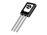
G A K
TO−225AA CASE 077 STYLE 2
MARKING DIAGRAM & PIN ASSIGNMENT
1. Cathode 2. Anode 3. Gate
YWW C106xxG
Y WW C106xx xx G
= Year = Work Week = Device Code = B, D, D1, M, M1 = Pb−Free Package
ORDERING INFORMATION
See detailed ordering and shipping information in the package dimensions section on page 2 of this data sheet.
*For additional information on our Pb−Free strategy and soldering details, please download the ON Semiconductor Soldering and Mounting Techniques Reference Manual, SOLDERRM/D.
© Semiconductor Components Industries, LLC, 2005
1
August, 2005 − Rev. 8
Publication Order Number: C106/D
�C106 Series
MAXIMUM RATINGS (TJ = 25°C unless otherwise noted)
Characteristic Peak Repetitive Off−State Voltage (Note 1) (Sine Wave, 50−60 Hz, RGK = 1 kW, TC = −40° to 110°C) C106B C106D, C106D1* C106M, C106M1* On-State RMS Current (180° Conduction Angles, TC = 80°C) Average On−State Current (180° Conduction Angles, TC = 80°C) Peak Non-Repetitive Surge Current (1/2 Cycle, Sine Wave, 60 Hz, TJ = +110°C) Circuit Fusing Considerations (t = 8.3 ms) Forward Peak Gate Power (Pulse Width v1.0 msec, TC = 80°C) Forward Average Gate Power (Pulse Width v1.0 msec, TC = 80°C) Forward Peak Gate Current (Pulse Width v1.0 msec, TC = 80°C) Operating Junction Temperature Range Storage Temperature Range IT(RMS) IT(AV) ITSM I2t PGM PG(AV) IGM TJ Tstg Symbol VDRM, VRRM 200 400 600 4.0 2.55 20 1.65 0.5 0.1 0.2 −40 to +110 −40 to +150 A A A A2s W W A °C °C Max Unit V
Mounting Torque (Note 2) 6.0 in. lb. − Maximum ratings are those values beyond which device damage can occur. Maximum ratings applied to the device are individual stress limit values (not normal operating conditions) and are not valid simultaneously. If these limits are exceeded, device functional operation is not implied, damage may occur and reliability may be affected. 1. VDRM and VRRM for all types can be applied on a continuous basis. Ratings apply for zero or negative gate voltage; however, positive gate voltage shall not be applied concurrent with negative potential on the anode. Blocking voltages shall not be tested with a constant current source such that the voltage ratings of the devices are exceeded. 2. Torque rating applies with use of compression washer (B52200F006). Mounting torque in excess of 6 in. lb. does not appreciably lower case-to-sink thermal resistance. Anode lead and heatsink contact pad are common.
THERMAL CHARACTERISTICS (TC = 25°C unless otherwise noted.)
Characteristic Thermal Resistance, Junction−to−Case Thermal Resistance, Junction−to−Ambient Maximum Lead Temperature for Soldering Purposes 1/8 in. from Case for 10 Seconds Symbol RqJC RqJA TL Max 3.0 75 260 Unit °C/W °C/W °C
ORDERING INFORMATION
Device C106B C106BG C106D C106DG C106D1* C106D1G* C106M C106MG C106M1* C106M1G* Package TO−225AA TO−225AA (Pb−Free) TO−225AA TO−225AA (Pb−Free) TO−225AA TO−225AA (Pb−Free) TO−225AA TO−225AA (Pb−Free) TO−225AA TO−225AA (Pb−Free) Shipping † 500 Units / Box 500 Units / Box 500 Units / Box 500 Units / Box 500 Units / Box 500 Units / Box 500 Units / Box 500 Units / Box 500 Units / Box 500 Units / Box
†For information on tape and reel specifications, including part orientation and tape sizes, please refer to our Tape and Reel Packaging Specifications Brochure, BRD8011/D. *D1 signifies European equivalent for D suffix and M1 signifies European equivalent for M suffix.
http://onsemi.com
2
�C106 Series
ELECTRICAL CHARACTERISTICS (TC = 25°C unless otherwise noted.)
Characteristic OFF CHARACTERISTICS Peak Repetitive Forward or Reverse Blocking Current (VAK = Rated VDRM or VRRM, RGK = 1000 Ohms) ON CHARACTERISTICS Peak Forward On−State Voltage (Note 3) (ITM = 4 A) Gate Trigger Current (Continuous dc) (Note 4) (VAK = 6 Vdc, RL = 100 Ohms) Peak Reverse Gate Voltage (IGR = 10 mA) Gate Trigger Voltage (Continuous dc) (Note 4) (VAK = 6 Vdc, RL = 100 Ohms) Gate Non−Trigger Voltage (Continuous dc) (Note 4) (VAK = 12 V, RL = 100 Ohms, TJ = 110°C) Latching Current (VAK = 12 V, IG = 20 mA) Holding Current (VD = 12 Vdc) (Initiating Current = 20 mA, Gate Open) TJ = 25°C TJ = −40°C TJ = 25°C TJ = −40°C TJ = +110°C TJ = 25°C TJ = −40°C TJ = 25°C TJ = −40°C VTM IGT − − VGRM VGT 0.4 0.5 VGD IL − − IH − − − 0.19 0.33 0.07 3.0 6.0 2.0 0.20 0.35 5.0 7.0 mA 0.2 0.60 0.75 − 0.8 1.0 − V mA − 15 35 − 200 500 6.0 V V − − 2.2 V mA TJ = 25°C TJ = 110°C IDRM, IRRM − − − − 10 100 mA mA Symbol Min Typ Max Unit
DYNAMIC CHARACTERISTICS Critical Rate−of−Rise of Off−State Voltage (VAK = Rated VDRM, Exponential Waveform, RGK = 1000 Ohms, TJ = 110°C) 3. Pulse Test: Pulse Width ≤ 2.0 ms, Duty Cycle ≤ 2%. 4. RGK is not included in measurement. dv/dt − 8.0 − V/ms
Voltage Current Characteristic of SCR
+ Current Anode + VTM on state IRRM at VRRM IH
Symbol
VDRM IDRM VRRM IRRM VTM IH
Parameter
Peak Repetitive Off State Forward Voltage Peak Forward Blocking Current Peak Repetitive Off State Reverse Voltage Peak Reverse Blocking Current Peak On State Voltage Holding Current Reverse Blocking Region (off state) Reverse Avalanche Region Anode −
+ Voltage IDRM at VDRM Forward Blocking Region (off state)
http://onsemi.com
3
�C106 Series
P(AV), AVERAGE ON-STATE POWER DISSIPATION (WATTS) 110 100 TC, CASE TEMPERATURE (° C) 90 80 70 60 50 40 30 20 10 HALF SINE WAVE RESISTIVE OR INDUCTIVE LOAD. 50 to 400 Hz DC 10 8 6 4 2 0 JUNCTION TEMPERATURE ≈ 110°C
HALF SINE WAVE RESISTIVE OR INDUCTIVE LOAD 50 TO 400Hz. DC
0
.4
.8
1.2
1.6
2.0
2.4
2.8
3.2
3.6
4.0
0
.4
.8
1.2
1.6
2.0
2.4
2.6
3.2
3.6
4.0
IT(AV) AVERAGE ON-STATE CURRENT (AMPERES)
IT(AV) AVERAGE ON-STATE CURRENT (AMPERES)
Figure 1. Average Current Derating
Figure 2. Maximum On−State Power Dissipation
100 IGT, GATE TRIGGER CURRENT (m A)
1000 IH, HOLDING CURRENT (m A) −10 5 20 35 50 65 80 95 110
10
100
1 −40 −25
10 −40 −25
−10
5
20
35
50
65
80
95
110
TJ, JUNCTION TEMPERATURE (°C)
TJ, JUNCTION TEMPERATURE (°C)
Figure 3. Typical Gate Trigger Current versus Junction Temperature
1.0 VGT , GATE TRIGGER VOLTAGE (V) 0.9 0.8 0.7 0.6 0.5 0.4 0.3 0.2 −45 −25 −10 5 20 35 50 65 80 95 110 1000 I L , LATCHING CURRENT (m A)
Figure 4. Typical Holding Current versus Junction Temperature
100
10 −40 −25
−10
5
20
35
50
65
80
95
110
TJ, JUNCTION TEMPERATURE (°C)
TJ, JUNCTION TEMPERATURE (°C)
Figure 5. Typical Gate Trigger Voltage versus Junction Temperature
Figure 6. Typical Latching Current versus Junction Temperature
http://onsemi.com
4
�C106 Series
PACKAGE INTERCHANGEABILITY The dimensional diagrams below compare the critical dimensions of the ON Semiconductor C-106 package with competitive devices. It has been demonstrated that the smaller dimensions of the ON Semiconductor package make it compatible in most lead-mount and chassis-mount applications. The user is advised to compare all critical dimensions for mounting compatibility.
.295 ____ .305 .145 ____ .155 .148 ____ .158 .425 ____ .435 123 .050 ____ .095
.115 ____ .130
.095 ____ .105
.400 ____ .360 .135 ____ .115
.127 ____ DIA .123
.026 ____ .019
5_ TYP .385 ____ .365
.520 ____ .480 .315 ____ .285 .420 ____ .400 .015 ____ .025 .045 ____ .055 .105 ____ .095 .054 ____ .046 .105 ____ .095
.575 ____ .655
.040 .094 BSC .025 ____ .035
.190 ____ .170
.020 ____ .026
ON Semiconductor C-106 Package
Competitive C-106 Package
http://onsemi.com
5
�C106 Series
PACKAGE DIMENSIONS
TO−225 CASE 77−09 ISSUE Z
−B− U Q −A−
123 NOTES: 1. DIMENSIONING AND TOLERANCING PER ANSI Y14.5M, 1982. 2. CONTROLLING DIMENSION: INCH. 3. 077−01 THRU −08 OBSOLETE, NEW STANDARD 077−09. INCHES MIN MAX 0.425 0.435 0.295 0.305 0.095 0.105 0.020 0.026 0.115 0.130 0.094 BSC 0.050 0.095 0.015 0.025 0.575 0.655 5_ TYP 0.148 0.158 0.045 0.065 0.025 0.035 0.145 0.155 0.040 −−− MILLIMETERS MIN MAX 10.80 11.04 7.50 7.74 2.42 2.66 0.51 0.66 2.93 3.30 2.39 BSC 1.27 2.41 0.39 0.63 14.61 16.63 5 _ TYP 3.76 4.01 1.15 1.65 0.64 0.88 3.69 3.93 1.02 −−−
F M
C
H
K
V G S D 2 PL 0.25 (0.010)
M
J R 0.25 (0.010) A
M
A
M
M
B
M
B
M
DIM A B C D F G H J K M Q R S U V
STYLE 2: PIN 1. CATHODE 2. ANODE 3. GATE
ON Semiconductor and are registered trademarks of Semiconductor Components Industries, LLC (SCILLC). SCILLC reserves the right to make changes without further notice to any products herein. SCILLC makes no warranty, representation or guarantee regarding the suitability of its products for any particular purpose, nor does SCILLC assume any liability arising out of the application or use of any product or circuit, and specifically disclaims any and all liability, including without limitation special, consequential or incidental damages. “Typical” parameters which may be provided in SCILLC data sheets and/or specifications can and do vary in different applications and actual performance may vary over time. All operating parameters, including “Typicals” must be validated for each customer application by customer’s technical experts. SCILLC does not convey any license under its patent rights nor the rights of others. SCILLC products are not designed, intended, or authorized for use as components in systems intended for surgical implant into the body, or other applications intended to support or sustain life, or for any other application in which the failure of the SCILLC product could create a situation where personal injury or death may occur. Should Buyer purchase or use SCILLC products for any such unintended or unauthorized application, Buyer shall indemnify and hold SCILLC and its officers, employees, subsidiaries, affiliates, and distributors harmless against all claims, costs, damages, and expenses, and reasonable attorney fees arising out of, directly or indirectly, any claim of personal injury or death associated with such unintended or unauthorized use, even if such claim alleges that SCILLC was negligent regarding the design or manufacture of the part. SCILLC is an Equal Opportunity/Affirmative Action Employer. This literature is subject to all applicable copyright laws and is not for resale in any manner.
PUBLICATION ORDERING INFORMATION
LITERATURE FULFILLMENT: N. American Technical Support: 800−282−9855 Toll Free Literature Distribution Center for ON Semiconductor USA/Canada P.O. Box 61312, Phoenix, Arizona 85082−1312 USA Phone: 480−829−7710 or 800−344−3860 Toll Free USA/Canada Japan : ON Semiconductor, Japan Customer Focus Center 2−9−1 Kamimeguro, Meguro−ku, Tokyo, Japan 153−0051 Fax: 480−829−7709 or 800−344−3867 Toll Free USA/Canada Phone: 81−3−5773−3850 Email: orderlit@onsemi.com ON Semiconductor Website: http://onsemi.com Order Literature: http://www.onsemi.com/litorder For additional information, please contact your local Sales Representative.
http://onsemi.com
6
C106/D
�


 工商网监
湘ICP备2023018690号
工商网监
湘ICP备2023018690号
