ON Semiconductor
Is Now
To learn more about onsemi™, please visit our website at
www.onsemi.com
onsemi and and other names, marks, and brands are registered and/or common law trademarks of Semiconductor Components Industries, LLC dba “onsemi” or its affiliates and/or
subsidiaries in the United States and/or other countries. onsemi owns the rights to a number of patents, trademarks, copyrights, trade secrets, and other intellectual property. A listing of onsemi
product/patent coverage may be accessed at www.onsemi.com/site/pdf/Patent-Marking.pdf. onsemi reserves the right to make changes at any time to any products or information herein, without
notice. The information herein is provided “as-is” and onsemi makes no warranty, representation or guarantee regarding the accuracy of the information, product features, availability, functionality,
or suitability of its products for any particular purpose, nor does onsemi assume any liability arising out of the application or use of any product or circuit, and specifically disclaims any and all
liability, including without limitation special, consequential or incidental damages. Buyer is responsible for its products and applications using onsemi products, including compliance with all laws,
regulations and safety requirements or standards, regardless of any support or applications information provided by onsemi. “Typical” parameters which may be provided in onsemi data sheets and/
or specifications can and do vary in different applications and actual performance may vary over time. All operating parameters, including “Typicals” must be validated for each customer application
by customer’s technical experts. onsemi does not convey any license under any of its intellectual property rights nor the rights of others. onsemi products are not designed, intended, or authorized
for use as a critical component in life support systems or any FDA Class 3 medical devices or medical devices with a same or similar classification in a foreign jurisdiction or any devices intended for
implantation in the human body. Should Buyer purchase or use onsemi products for any such unintended or unauthorized application, Buyer shall indemnify and hold onsemi and its officers, employees,
subsidiaries, affiliates, and distributors harmless against all claims, costs, damages, and expenses, and reasonable attorney fees arising out of, directly or indirectly, any claim of personal injury or death
associated with such unintended or unauthorized use, even if such claim alleges that onsemi was negligent regarding the design or manufacture of the part. onsemi is an Equal Opportunity/Affirmative
Action Employer. This literature is subject to all applicable copyright laws and is not for resale in any manner. Other names and brands may be claimed as the property of others.
�CAT5120, CAT5121,
CAT5122
16‐tap Digital
Potentiometers (POTs)
with 2‐wire Interface
http://onsemi.com
Description
CAT5120/5121/5122 linear-taper digital POTs perform the same
function as a mechanical potentiometer or a variable resistor. These
devices consist of a fixed resistor and a wiper contact with 16-tap
points that are digitally controlled through a 2-wire up/down serial
interface.
The CAT5120 is configured as a potentiometer. The CAT5121 and
CAT5122 are configured as variable resistors. See Pin Configurations
for part functionality.
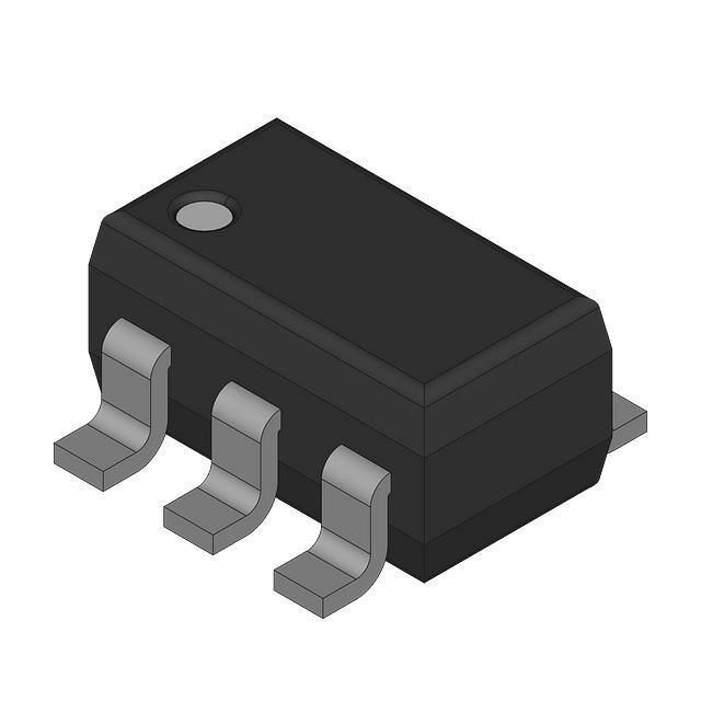
Two resistance values are available: 10 kW and 50 kW. These are
available in space-saving 5-pin and 6-pin SC−70 and SOT−23
packages.
Features
0.3 mA Ultra-low Standby Current
Single-supply Operation: 2.7 V to 5.5 V
Glitchless Switching between Resistor Taps
Power-on Reset to Midscale
2-wire Up/Down Serial Interface
Resistance Values: 10 kW, 50 kW
Available in SC−70 and SOT−23 Packages
These Devices are Pb-Free, Halogen Free/BFR Free and are RoHS
Compliant
SC−70
SD SUFFIX
CASE 419AD
SOT−23
TB SUFFIX
CASE 527AJ
SC−70
SD SUFFIX
CASE 419AC
SOT−23
TB SUFFIX
CASE 527AH
PIN CONFIGURATIONS
SC−70
SOT−23
VDD 1
6 H
GND 2
5 W
U/D 3
4 CS
SC−70
SOT−23
Applications
CAT5120
LCD Screen Adjustment
Volume Control
Mechanical Potentiometer Replacement
Gain Adjustment
Line Impedance Matching
VDD
6 H
1
GND 2
5 L
CAT5121
4 CS
U/D 3
SC−70
SOT−23
5 H
VDD 1
GND 2
CAT5122
U/D 3
4 CS
ORDERING INFORMATION
See detailed ordering and shipping information in the package
dimensions section on page 7 of this data sheet.
Semiconductor Components Industries, LLC, 2013
July, 2013 − Rev. 8
1
Publication Order Number:
CAT5120/D
�CAT5120, CAT5121, CAT5122
H
VDD
UP−DOWN
COUNTER
CS
U/D
16−POSITION
DECODER
GND
W
L
Figure 1. Functional Diagram
Table 1. PIN DESCRIPTIONS
Name
Description
VDD
Power Supply
GND
Ground
U/D
Up/Down Control Input. With CS low, a low-to-high transition increments or decrements the wiper position.
CS
Chip Select Input. A high-to-low CS transition determines the mode: increment if U/D is high, or decrement if U/D is low.
L
Low Terminal of Resistor
W
Wiper Terminal of Resistor
H
High Terminal of Resistor
Table 2. ABSOLUTE MAXIMUM RATINGS
Parameters
Ratings
Units
−0.3 to +6
V
−0.3 to (VDD + 0.3)
V
Input and Output Latch-up Immunity
200
mA
Maximum Continuous Current into H, L and W
50 kW
ą10 kW
1.3
1.3
Continuous Power Dissipation (TA = +70C)
5-pin SC−70 (Note 1)
6-pin SC−70 (Note 1)
247
245
VDD to GND
All Other Pins to GND
mA
Operating Temperature Range
Junction Temperature
Storage Temperature Range
Soldering Temperature (soldering, 10 s)
mW
−40 to +85
C
+150
C
−65 to +150
C
+300
C
Stresses exceeding Maximum Ratings may damage the device. Maximum Ratings are stress ratings only. Functional operation above the
Recommended Operating Conditions is not implied. Extended exposure to stresses above the Recommended Operating Conditions may affect
device reliability.
1. Derate 3.1 mW/C above TA = +70C
http://onsemi.com
2
�CAT5120, CAT5121, CAT5122
Table 3. ELECTRICAL CHARACTERISTICS
(VDD = 2.7 V to 5.5 V, VH = VDD, VL = 0, TA = −40C to +85C. Typical values are at VDD = 2.7 V, TA = 25C, unless otherwise noted.)
Parameter
Symbol
Conditions
Min
Typ
Max
Units
DC PERFORMANCE
16
Resolution
Taps
End-to-End Resistance (−50)
37.5
50
62.5
End-to-End Resistance (−10)
7.5
10
12.5
End-to-End Resistance Tempco
TCR
200
Ratiometric Resistance Tempco
kW
ppm/C
5
ppm/C
Integral Non-linearity
INL
0.5
LSB
Differential Non-linearity
DNL
0.5
LSB
0.1
0.5
LSB
200
600
W
Zero/Full-Scale Error
Wiper Resistance
RW
DIGITAL INPUTS
Input High Voltage
VIH
Input Low Voltage
VIL
0.7 x VDD
V
0.3 x VDD
V
TIMING CHARACTERISTICS (Figures 7, 8)
U/D Mode to CS Setup
tCU
25
ns
CS to U/D Step Setup
tCI
50
ns
CS to U/D Step Hold
tIC
25
ns
U/D Step Low Period
tIL
25
ns
tIH
25
U/D Step High Period
Up/Down Toggle Rate (Note 2)
fTOGGLE
Output Settling Time (Note 3)
tSETTLE
ns
1
MHz
50 kW variable resistor
configuration, CL = 10 pF
1
ms
50 kW potentiometer
configuration, CL = 10 pF
0.25
POWER SUPPLY
Supply Voltage
VDD
Active Supply Current (Note 4)
IDD
Standby Supply Current (Note 5)
ISB
2.
3.
4.
5.
2.7
VDD = +5 V
Up/Down Toggle Rate: fTOGGLE = 1 / tSETTLE
Typical settling times are dependent on end-to-end resistance.
Supply current measured while changing wiper tap, fTOGGLE = 1 MHz.
Supply current measured while wiper position is fixed.
http://onsemi.com
3
0.3
5.5
V
25
mA
1
mA
�CAT5120, CAT5121, CAT5122
TYPICAL OPERATING CHARACTERISTICS
(TA = 25C, unless otherwise noted.)
1.5
200
END−TO−END RESISTANCE
CHANGE (%)
WIPER RESISTANCE (W)
250
VDD = 2.7 V
150
VDD = 5.5 V
100
50
0
0
4
8
12
16
20
24
28
50 K
0
−0.5
−1.0
−1.5
0
50
100
150
WIPER POSITION
TEMPERATURE (C)
Figure 2. Wiper Resistance vs. Tap Position
Figure 3. Change in End-to-End Resistance vs.
Temperature
0.45
0.40
100
80
60
50 k
40
VDD = 5.5 V
0.35
100 k
CURRENT (mA)
RESISTANCE (kW)
0.5
−2.0
−50
32
120
0.30
VDD = 2.7 V
0.25
0.20
0.15
0.10
20
0
1.0
0.05
10 k
1 3
5
7
0
−50
9 11 13 15 17 19 21 23 25 27 29 31
0
50
100
TAP POSITION
TEMPERATURE (C)
Figure 4. W-to-L Resistance vs. Tap Position
Figure 5. Supply Current vs. Temperature
U/D
2 V/div
Wiper
Output
100 mV/div
200 ns/div
Figure 6. Tap-to-Tap Switching Transient
http://onsemi.com
4
150
�CAT5120, CAT5121, CAT5122
FUNCTIONAL DESCRIPTION
The CAT5120/5121/5122 consist of a fixed resistor and a
wiper contact with 16-tap points that are digitally controlled
through a 2-wire up/down serial interface. Two end-to-end
resistance values are available: 10 kW and 50 kW.
The CAT5120 is designed to operate as a potentiometer.
In this configuration, the low terminal of the resistor array
is connected to ground (pin 2).
The CAT5122 performs as a variable resistor. In this
device, the wiper terminal and high terminal of the resistor
array is connected at pin 5. The CAT5121 is a similar
variable resistor, except the low terminal is connected to
pin 5.
low, the part will go into increment mode if U/D input is
high, and into decrement mode when U/D input is low. Once
the mode is set, the device will remain in that mode until CS
goes high again. A low-to-high transition at the U/D pin will
increment or decrement the wiper position depending on the
current mode (Figures 7 and 8).
When the CS input transitions to high (serial interface
inactive), the value of the counter is stored and the wiper
position is maintained.
Note that when the wiper reaches the maximum (or
minimum) tap position, the wiper will not wrap around to the
minimum (or maximum) position.
Digital Interface Operation
Power-on Reset
The devices have two modes of operation when the serial
interface is active: increment and decrement mode. The
serial interface is only active when CS is low.
The CS and U/D inputs control the position of the wiper
along the resistor array. When CS transitions from high to
All parts in this family feature power-on reset (POR)
circuitry that sets the wiper position to midscale at
power-up. By default, the chip is in the increment mode.
CS
tCU
tIC
tIL
U/D
tIH
tCI
tSETTLE
tSETTLE
W
Note: “W” is not a digital signal. It represents wiper transitions.
Figure 7. Serial Interface Timing Diagram, Increment Mode
CS
tCU
tIC
tIH
U/D
tIL
W
tCI
tSETTLE
tSETTLE
Note: “W” is not a digital signal. It represents wiper transitions.
Figure 8. Serial Interface Timing Diagram, Decrement Mode
http://onsemi.com
5
�CAT5120, CAT5121, CAT5122
APPLICATIONS INFORMATION
Adjustable Gain
The devices are intended for circuits requiring digitally
controlled adjustable resistance, such as LCD contrast
control, where voltage biasing adjusts the display contrast.
Figures 11 and 12 show how to use the variable resistor to
digitally adjust the gain of a noninverting op amp
configuration. Connect the CAT5121 in series with a resistor
to ground to form the adjustable gain control of a
noninverting amplifier. The devices have a low 5 ppm/C
ratiometric tempco that allows for a very stable adjustable
gain configuration over temperature.
Alternative Positive LCD Bias Control
Use an op amp to provide buffering and gain on the output
of the CAT5120. Connect the mechanical potentiometer to
the positive input of a noninverting op amp (Figure 9) to
select a portion of the input signal by digitally controlling the
wiper terminal. Figure 10 shows a similar circuit for the
CAT5121.
+5 V
+5 V
H
H
W
CAT5120
30 V
30 V
VOUT
VOUT
L
L
CAT5121
Figure 9. Positive LCD Bias Control
Figure 10. Positive LCD Bias Control
VCC
VCC
VIN
VIN
VOUT
VOUT
H
L
CAT5121
W
H
CAT5120
L
Figure 11. Adjustable Gain Circuit
Figure 12. Adjustable Gain Circuit
http://onsemi.com
6
�CAT5120, CAT5121, CAT5122
Table 4. ORDERING INFORMATION
Resistor [kW]
Package
Shipping†
CAT5120SDI−10GT3
10
SC70−6
(Pb−Free)
3000 / Tape & Reel
CAT5120TBI−10GT3
10
SOT23−6
(Pb−Free)
3000 / Tape & Reel
CAT5120SDI−50GT3
50
SC70−6
(Pb−Free)
3000 / Tape & Reel
CAT5120TBI−50GT3
50
SOT23−6
(Pb−Free)
3000 / Tape & Reel
CAT5121SDI−10GT3
10
SC70−6
(Pb−Free)
3000 / Tape & Reel
CAT5121TBI−10GT3
10
SOT23−6
(Pb−Free)
3000 / Tape & Reel
CAT5121SDI−50GT3
50
SC70−6
(Pb−Free)
3000 / Tape & Reel
CAT5121TBI−50GT3
50
SOT23−6
(Pb−Free)
3000 / Tape & Reel
CAT5122SDI−10GT3
10
SC70−5
(Pb−Free)
3000 / Tape & Reel
CAT5122TBI−10GT3
10
SOT23−5
(Pb−Free)
3000 / Tape & Reel
CAT5122SDI−50GT3
50
SC70−5
(Pb−Free)
3000 / Tape & Reel
CAT5122TBI−50GT3
50
SOT23−5
(Pb−Free)
3000 / Tape & Reel
Orderable Part Number
†For information on tape and reel specifications, including part orientation and tape sizes, please refer to our Tape and Reel Packaging
Specifications Brochure, BRD8011/D.
6. For detailed information and a breakdown of device nomenclature and numbering systems, please see the ON Semiconductor Device
Nomenclature document, TND310/D, available at www.onsemi.com.
http://onsemi.com
7
�CAT5120, CAT5121, CAT5122
PACKAGE DIMENSIONS
SC−88 (SC−70 6 Lead), 1.25x2
CASE 419AD
ISSUE A
SYMBOL
D
e
e
E1 E
MIN
MAX
A
0.80
1.10
A1
0.00
0.10
A2
0.80
1.00
b
0.15
0.30
c
0.10
0.18
D
1.80
2.00
2.20
E
1.80
2.10
2.40
E1
1.15
1.25
1.35
0.65 BSC
e
L
TOP VIEW
NOM
0.26
0.36
L1
0.42 REF
L2
0.15 BSC
0.46
θ
0º
8º
θ1
4º
10º
q1
A2 A
q
q1
b
L
L1
A1
SIDE VIEW
c
END VIEW
Notes:
(1) All dimensions are in millimeters. Angles in degrees.
(2) Complies with JEDEC MO-203.
http://onsemi.com
8
L2
�CAT5120, CAT5121, CAT5122
PACKAGE DIMENSIONS
SOT−23, 6 Lead
CASE 527AJ
ISSUE B
D
A
NOTES:
1. DIMENSIONING AND TOLERANCING PER
ASME Y14.5M, 1994.
2. CONTROLLING DIMENSION: MILLIMETERS.
3. DATUM C IS THE SEATING PLANE.
B
6
5
4
1
2
3
E
E1
GAGE
PLANE
6X
e
TOP VIEW
L2
b
0.20
SEATING
PLANE
L
M
C A
S
B
S
DETAIL A
A2
c
A
6X
0.10 C
A1
SIDE VIEW
C
SEATING
PLANE
DETAIL A
END VIEW
RECOMMENDED
SOLDERING FOOTPRINT*
3.30
6X
0.85
6X
0.56
0.95
PITCH
DIMENSIONS: MILLIMETERS
*For additional information on our Pb−Free strategy and soldering
details, please download the ON Semiconductor Soldering and
Mounting Techniques Reference Manual, SOLDERRM/D.
http://onsemi.com
9
DIM
A
A1
A2
b
c
D
E
E1
e
L
L2
MILLIMETERS
MIN
MAX
--1.45
0.00
0.15
0.90
1.30
0.20
0.50
0.08
0.26
2.70
3.00
2.50
3.10
1.30
1.80
0.95 BSC
0.20
0.60
0.25 BSC
�CAT5120, CAT5121, CAT5122
PACKAGE DIMENSIONS
SC−88A (SC−70 5 Lead), 1.25x2
CASE 419AC
ISSUE A
SYMBOL
MIN
A
0.80
1.10
A1
0.00
0.10
A2
0.80
1.00
b
0.15
0.30
c
0.10
0.18
D
1.80
2.00
2.20
E
1.80
2.10
2.40
E1
1.15
1.25
1.35
D
e
e
E1 E
e
MAX
0.65 BSC
L
TOP VIEW
NOM
0.26
0.36
L1
0.42 REF
L2
0.15 BSC
0.46
θ
0º
8º
θ1
4º
10º
q1
A2 A
q
q1
b
L
L1
A1
SIDE VIEW
c
END VIEW
Notes:
(1) All dimensions are in millimeters. Angles in degrees.
(2) Complies with JEDEC MO-203.
http://onsemi.com
10
L2
�CAT5120, CAT5121, CAT5122
PACKAGE DIMENSIONS
SOT−23, 5 Lead
CASE 527AH
ISSUE O
D
SYMBOL
E1
MIN
NOM
0.90
1.45
A1
0.00
0.15
A2
0.90
b
0.30
0.50
c
0.08
0.22
E
1.15
D
2.90 BSC
E
2.80 BSC
E1
1.60 BSC
e
e
L
1.30
0.95 BSC
0.45
0.30
L1
PIN #1 IDENTIFICATION
MAX
A
0.60
0.60 REF
L2
0.25 REF
θ
0°
4°
8°
θ1
5°
10°
15°
θ2
5°
10°
15°
TOP VIEW
θ1
A2
A
θ
b
θ2
L1
A1
SIDE VIEW
L2
L
c
END VIEW
Notes:
(1) All dimensions in millimeters. Angles in degrees.
(2) Complies with JEDEC standard MO-178.
ON Semiconductor and
are registered trademarks of Semiconductor Components Industries, LLC (SCILLC). SCILLC owns the rights to a number of patents, trademarks,
copyrights, trade secrets, and other intellectual property. A listing of SCILLC’s product/patent coverage may be accessed at www.onsemi.com/site/pdf/Patent−Marking.pdf. SCILLC
reserves the right to make changes without further notice to any products herein. SCILLC makes no warranty, representation or guarantee regarding the suitability of its products for any
particular purpose, nor does SCILLC assume any liability arising out of the application or use of any product or circuit, and specifically disclaims any and all liability, including without
limitation special, consequential or incidental damages. “Typical” parameters which may be provided in SCILLC data sheets and/or specifications can and do vary in different applications
and actual performance may vary over time. All operating parameters, including “Typicals” must be validated for each customer application by customer’s technical experts. SCILLC
does not convey any license under its patent rights nor the rights of others. SCILLC products are not designed, intended, or authorized for use as components in systems intended for
surgical implant into the body, or other applications intended to support or sustain life, or for any other application in which the failure of the SCILLC product could create a situation where
personal injury or death may occur. Should Buyer purchase or use SCILLC products for any such unintended or unauthorized application, Buyer shall indemnify and hold SCILLC and
its officers, employees, subsidiaries, affiliates, and distributors harmless against all claims, costs, damages, and expenses, and reasonable attorney fees arising out of, directly or indirectly,
any claim of personal injury or death associated with such unintended or unauthorized use, even if such claim alleges that SCILLC was negligent regarding the design or manufacture
of the part. SCILLC is an Equal Opportunity/Affirmative Action Employer. This literature is subject to all applicable copyright laws and is not for resale in any manner.
PUBLICATION ORDERING INFORMATION
LITERATURE FULFILLMENT:
Literature Distribution Center for ON Semiconductor
P.O. Box 5163, Denver, Colorado 80217 USA
Phone: 303−675−2175 or 800−344−3860 Toll Free USA/Canada
Fax: 303−675−2176 or 800−344−3867 Toll Free USA/Canada
Email: orderlit@onsemi.com
N. American Technical Support: 800−282−9855 Toll Free
USA/Canada
Europe, Middle East and Africa Technical Support:
Phone: 421 33 790 2910
Japan Customer Focus Center
Phone: 81−3−5817−1050
http://onsemi.com
11
ON Semiconductor Website: www.onsemi.com
Order Literature: http://www.onsemi.com/orderlit
For additional information, please contact your local
Sales Representative
CAT5120/D
�


 工商网监
湘ICP备2023018690号
工商网监
湘ICP备2023018690号
