CAT5136, CAT5137,
CAT5138
Digital Potentiometers (POTs)
with 128 Taps and
I2C Interface
http://onsemi.com
Description
CAT5136, CAT5137, and CAT5138 are a family of digital POTs
operating like mechanical potentiometers in various configurations.
The tap points between the 127 equal resistive elements are connected
to the wiper output via CMOS switches. The switches are controlled
by a 7-bit Wiper Control Register (WCR) via the I2C serial bus.
CAT5136 is configured as a variable resistor. CAT5137 and CAT5138
are resistive voltage dividers, with one terminal of the potentiometer
connected to GND. CAT5137 and CAT5138 have different device IDs,
which makes it possible to use both on the same I2C bus. Upon
power-up, the WCR is set to mid-scale (1000000).
Features
Single Linear Digital Potentiometer with 128 Taps
End-to-End Resistance of 10 kW, 50 kW and 100 kW
I2C Interface
Wiper goes to Midscale at Power-up
Digital Supply Range (VDD): 2.7 V to 5.5 V
Low Standby Current
Industrial Temperature Range: −40C to +85C
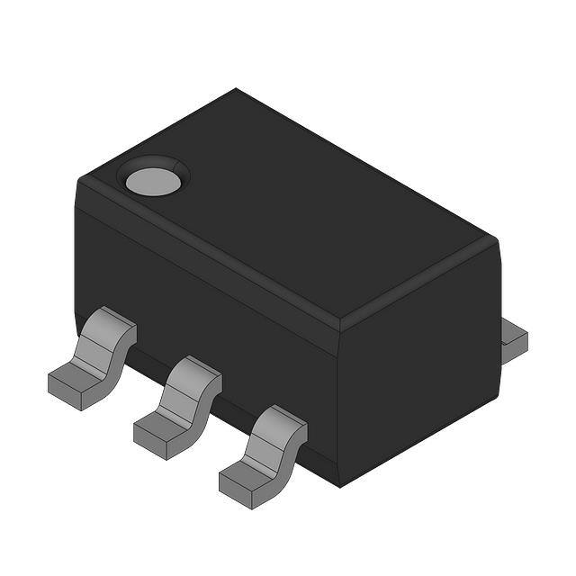
6-pin SC−70 Package
These Devices are Pb-Free, Halogen Free/BFR Free and are RoHS
Compliant
Typical Applications
July, 2013 − Rev. 1
PIN CONNECTIONS
(for low pin count devices)
VDD 1
6 RL
GND 2
5 RW
SCL 3
4
SDA
CAT5136
VDD
1
6 RH
GND
2
5 RW
SCL
3
4 SDA
CAT5137
CAT5138
(Top Views)
LCD Screen Adjustment
Volume Control
Mechanical Potentiometer Replacement
Gain Adjustment
Line Impedance Matching
VCOM Setting Adjustments
Semiconductor Components Industries, LLC, 2013
SC−70
SD SUFFIX
CASE 419AD
See detailed pin function descriptions on page 2.
ORDERING INFORMATION
See detailed ordering and shipping information in the package
dimensions section on page 9 of this data sheet.
1
Publication Order Number:
CAT5136/D
�CAT5136, CAT5137, CAT5138
VDD
SCL
SDA
VDD
I2C
Interface
and
Control
RW
Power On
Midscale
RL
SCL
SDA
RH
I2C
Interface
and
Control
RW
Power On
Midscale
GND
GND
(CAT5136)
(CAT5137, CAT5138)
Figure 1. Block Diagram
Table 1. PIN FUNCTION DESCRIPTION
Pin No.
CAT5136
CAT5137/CAT5138
Pin Name
1
1
VDD
Digital Supply Voltage (2.7 V to 5.5 V)
2
2
GND
Ground
3
3
SCL
Serial Bus Clock input for the I2C Serial Bus. This clock is used to clock all data
transfers into and out of the CAT5136−8
4
4
SDA
Serial Data Input/Output − Bidirectional Serial Data pin used to transfer data into
and out of the CAT5136−8. This is an Open-Drain I/O and can be wire OR’d with
other Open-Drain (or Open Collector) I/Os.
5
5
RW
Wiper Terminal for the potentiometer
6
−
RL
Low Reference Terminal for the potentiometer
−
6
RH
High Reference Terminal for the potentiometer
Description
Table 2. ABSOLUTE MAXIMUM RATINGS
Parameter
Symbol
Temperature Under Bias
Storage Temperature Range
TSTG
Range
Unit
−55 to +125
C
−65 to 150
C
Voltage on any SDA, SCL, A0 & A1 pins with respect to Ground (Note 1)
−0.3 to VDD + 0.3
V
Voltage on RH, RL & RW pins with respect to Ground
−0.3 to VDD + 0.3
V
−0.3 to +6
V
6
mA
+300
C
VDD with respect to Ground
Wiper Current (10 sec)
Lead Soldering temperature (10 sec)
Stresses exceeding Maximum Ratings may damage the device. Maximum Ratings are stress ratings only. Functional operation above the
Recommended Operating Conditions is not implied. Extended exposure to stresses above the Recommended Operating Conditions may affect
device reliability.
1. Latch-up protection is provided for stresses up to 100 mA on address and data pins from −0.3 V to VDD +0.3 V.
Table 3. RECOMMENDED OPERATION CONDITIONS
Parameter
Digital Supply Voltage
Operating Temperature Range
http://onsemi.com
2
Symbol
Value
Unit
VDD
+2.7 to +5.5
V
−40 to +85
C
�CAT5136, CAT5137, CAT5138
Table 4. POTENTIOMETERS CHARACTERISTICS (Over recommended operating conditions unless otherwise stated.)
Limits
Parameter
Symbol
Test Conditions
Min
Typ
Max
Units
Potentiometer Resistance (10 kW)
RPOT
10
kW
Potentiometer Resistance (50 kW)
RPOT
50
kW
Potentiometer Resistance (100 kW)
RPOT
100
Potentiometer Resistance Tolerance
RTOL
Power Rating
%
50
mW
3
mA
200
W
VDD
V
25C
Wiper Current
IW
Wiper Resistance
RW
Voltage on RW, RH or RL
kW
20
VTERM
VDD = 3.3 V
GND = 0 V; VDD = 2.7 V to +5.5 V
85
GND
Resolution
RES
Integral Non-Linearity (Note 3)
INL
VW(n)(actual) − VW(n)(expected)
(Notes 6, 7)
1
LSB
(Note 5)
Differential Non-Linearity (Note 4)
DNL
VW(n+1) − [VW(n)+LSB] (Notes 6, 7)
1
LSB
(Note 5)
Resistor Integral Non-Linearity
RINL
Rn − n*LSB (Notes 6, 8)
2
LSB
(Note 5)
Resistor Differential Non-Linearity
RDNL
Rn − [Rn−1 + LSB] (Notes 6, 8)
1
LSB
(Note 5)
Temperature Coefficient of RPOT
TCRPOT
(Note 2)
Ratiometric Temperature Coefficient
TCRatio
(Note 2)
CH/CL/CW
(Note 2)
Potentiometer Capacitances
Frequency Response
fc
0.78
%
ppm/C
300
30
ppm/C
10/10/25
pF
0.4
MHz
RPOT
2. This parameter is tested initially and after a design or process change that affects the parameter.
3. Integral Non-Linearity is utilized to determine actual wiper voltage versus expected voltage as determined by wiper position when used as
a potentiometer.
4. Differential Non-Linearity is utilized to determine the actual change in voltage between two successive tap positions when used as a
potentiometer.
5. LSB = (RHM − RLM)/127; where RHM and RLM are the highest and lowest measured values on the wiper terminal.
6. n = 1, 2, ..., 127
7. VDD @ RH; VW measured @ RW with no load.
8. Rw and RL in the range of 0 V and VDD.
Table 5. D.C. ELECTRICAL CHARACTERISTICS (Over recommended operating conditions unless otherwise stated.)
Parameter
Power Supply Current
(Write/Read)
Standby Current
Symbol
IDD
ISB(VDD)
Test Conditions
Min
Max
Units
FSCL = 400 kHz, SDA Open,
VDD = 5.5 V, Input = GND
200
mA
VIN = GND or VDD , SDA = VDD
0.5
mA
Input Leakage Current
ILI
VIN = GND to VDD
−1
1
mA
Output Leakage Current
ILO
VOUT = GND to VDD
−1
1
mA
Input Low Voltage
VIL
−0.3
VDD x 0.3
V
Input High Voltage
VIH
VDD x 0.7
VDD + 0.3
V
Output Low Voltage (VDD = 3.0 V)
VOL
0.4
V
IOL = 3 mA
http://onsemi.com
3
�CAT5136, CAT5137, CAT5138
Table 6. A.C. CHARACTERISTICS
Parameter (see Figure 6)
Symbol
Max
Units
FSCL
400
kHz
TI (Note 9)
50
ns
tAA
1
ms
Clock Frequency
Noise Suppression Time Constant at SCL & SDA Inputs
SCL Low to SDA Data Out and ACK Out
Time the bus must be free before a new transmission can start
Min
Typ
tBUF (Note 9)
1.2
ms
tHD:STA
0.6
ms
Clock Low Period
tLOW
1.2
ms
Clock High Period
tHIGH
0.6
ms
Start Condition Setup Time (for a Repeated Start Condition)
tSU:STA
0.6
ms
Data In Setup Time
tSU:DAT
100
ns
tHD:DAT
0
Start Condition Hold Time
Data in Hold Time
ms
SDA and SCL Rise Time
tR (Note 9)
0.3
ms
SDA and SCL Fall Time
tF (Note 9)
300
ns
Stop Conditions Setup Time
tSU:STO
0.6
ms
tDH
100
ns
Data Out Hold Time
9. This parameter is tested initially and after a design or process change that affects the parameter.
Table 7. CAPACITANCE (TA = 25C, f = 1.0 MHz, VDD = 5.0 V)
Parameter
Input/Output Capacitance (SDA, SDC)
Symbol
Test Conditions
CI/O
VI/O = 0 V (Note 10)
Min
Typ
Max
Unit
10
pF
10. This parameter is tested initially and after a design or process change that affects the parameter.
Table 8. POWER-UP TIMING (Notes 11, 12)
Symbol
Parameter
Min
Max
Units
tPUR
Power-up to Read Operation
1
ms
tPUW
Power-up to Write Operation
1
ms
Min
Max
Units
Wiper Response Time After Power Supply Stable
5
10
ms
Wiper Response Time After Instruction Issued
5
10
ms
11. This parameter is tested initially and after a design or process change that affects the parameter.
12. tPUR and tPUW are the delays required from the time VDD is stable until the specified operation can be initiated.
Table 9. WIPER TIMING
Symbol
tWRPO
tWRL
Parameter
http://onsemi.com
4
�CAT5136, CAT5137, CAT5138
TYPICAL PERFORMANCE CHARACTERISTICS
90
60
VCC = 2.7 V
VCC = 5.5 V
50
ICC (mA)
RWL (kW)
40
30
20
0
16
32
48
25C
60
90C
50
125C
40
64
80
96
112
10
0
128
2
3
4
5
TAP POSITION
VCC (V)
Figure 2. Resistance between RW and RL
Figure 3. Power Supply Current
6
1.0
0.8
Potentiometer Configuration
0.8
Potentiometer Configuration
TA = +25C, RPOT = 10 kW
0.6
0.6
0.4
0.4
DNL (LSB)
INL (LSB)
70
20
Rheostat Configuration
TA = +25C, RPOT = 50 kW
1.0
0.2
0
−0.2
0.2
0
−0.2
−0.4
−0.4
−0.6
−0.8
−1.0
−40C
30
10
0
80
−0.6
VCC = 2.7 V
VCC = 5.5 V
0
16
32
48
64
80
96
112
−0.8
−1.0
128
VCC = 2.7 V
VCC = 5.5 V
0
16
32
48
64
80
96
112
TAP POSITION
TAP POSITION
Figure 4. Integral Non−Linearity
Figure 5. Differential Non−Linearity
tHIGH
tF
tLOW
tR
tLOW
SCL
tSU:STA
tHD:STA
tHD:DAT
tSU:DAT
tSU:STO
SDA IN
tAA
tDH
SDA OUT
Figure 6. Bus Timing
http://onsemi.com
5
tBUF
128
�CAT5136, CAT5137, CAT5138
SERIAL BUS PROTOCOL
The following defines the features of the I2C bus protocol:
1. Data transfer may be initiated only when the bus is
not busy.
2. During a data transfer, the data line must remain
stable whenever the clock line is high. Any
changes in the data line while the clock is high
will be interpreted as a START or STOP condition.
STOP Condition
A LOW to HIGH transition of SDA when SCL is HIGH
determines the STOP condition. All operations must end
with a STOP condition (see Figure 7).
Acknowledge
After a successful data transfer, each receiving device is
required to generate an acknowledge. The acknowledging
device pulls down the SDA line during the ninth clock cycle,
signaling that it received the 8 bits of data (see Figure 8).
The CAT513x responds with an acknowledge after
receiving a START condition and its slave address. If the
device has been selected along with a write operation, it
responds with an acknowledge after receiving each 8-bit
byte.
When the CAT513x is in a READ mode it transmits 8 bits
of data, releases the SDA line, and monitors the line for an
acknowledge. Once it receives this acknowledge, the
CAT513x will continue to transmit data. If no acknowledge
is sent by the Master, the device terminates data transmission
and waits for a STOP condition.
The device controlling the transfer is a master, typically a
processor or controller, and the device being controlled is the
slave. The master will always initiate data transfers and
provide the clock for both transmit and receive operations.
Therefore, the CAT513x will be considered a slave device
in all applications.
START Condition
The START Condition precedes all commands to the
device, and is defined as a HIGH to LOW transition of SDA
when SCL is HIGH. The CAT513x monitors the SDA and
SCL lines and will not respond until this condition is met
(see Figure 7).
SDA
SCL
START CONDITION
STOP CONDITION
Figure 7. Start/Stop Condition
BUS RELEASE DELAY (TRANSMITTER)
SCL FROM
MASTER
1
8
BUS RELEASE DELAY (RECEIVER)
9
DATA OUTPUT
FROM TRANSMITTER
DATA OUTPUT
FROM RECEIVER
START
ACK DELAY ( tAA)
Figure 8. Acknowledge Condition
http://onsemi.com
6
ACK SETUP ( tSU:DAT)
�CAT5136, CAT5137, CAT5138
DEVICE DESCRIPTION
Slave Address Instruction Byte Description
Only the device with slave address matching the input
byte will be accessed by the master.
The last bit is the READ/WRITE bit and determines the
function to be performed. If it is a “1” a read command is
initiated and if it is a “0” a write is initiated.
After the Master sends a START condition and the slave
address byte, the CAT513x monitors the bus and responds
with an acknowledge when its address matches the
transmitted slave address.
The first byte sent to the CAT513x from the master
processor is called the Slave Address Byte. The most
significant seven bits of the slave address are a device type
identifier. For CAT5136 and CAT5137 these bits are fixed
at 0101110. For CAT5138, they are 0111110. This allows
both CAT5137 and CAT5138, which are functionally
identical, to reside on the same bus (refer to Table 10).
Table 10. BYTE 1 SLAVE ADDRESS AND INSTRUCTION BYTE
Device Type Identifier
Device
ID6
ID5
ID4
ID3
ID2
ID1
ID0
Read/Write
CAT5136
0
1
0
1
1
1
0
R/W
CAT5137
0
1
0
1
1
1
0
R/W
CAT5138
0
1
1
1
1
1
0
R/W
(MSB)
(LSB)
Wiper Control Register (WCR) Description
A write operation (see Table 11) requires a Start condition,
followed by a valid slave address byte, a valid address byte
00h, a data byte and a STOP condition. After each of the
three bytes, the CAT513x responds with an acknowledge.
After the third byte, the data is written to the Wiper Control
Register, and the wiper changes position accordingly.
A read operation (see Table 12) requires a Start condition,
followed by a valid slave address byte for write, a valid
address byte 00h, a second START and a second slave
address byte for read. After each of the three bytes, the
CAT513x responds with an acknowledge and then the
device transmits the data byte. The master terminates the
read operation by issuing a STOP condition following the
last bit of Data byte.
The CAT513x contains a 7-bit volatile Wiper Control
Register which is decoded to select one of the 128 switches
along its resistor array. The Wiper Control Register loses its
contents when the CAT513x is powered-down. At
power-up, the register is loaded with the midscale value 40h.
The contents of the WCR may be read or changed directly
by the host using a READ/WRITE command on the I2C bus
(see Table 1 to access WCR). Since the CAT513x will only
make use of the 7 LSB bits, the first data bit, or MSB, is
ignored on write instructions and will always come back as
a “0” on read commands.
Table 11. WRITE OPERATION
CAT5136 and CAT5137
STOP
DATA BYTE IN
ACK
ADDRESS
BYTE
3rd byte
ACK
Wb
SLAVE
ADDRESS
2nd byte
ACK
START
1st byte
S 0 1 0 1 1 1 0 0 A 0 0 0 0 0 0 0 0 A X D6 D5 D4 D3 D2 D1 D0 A P
STOP
DATA BYTE IN
ACK
ADDRESS
BYTE
3rd byte
ACK
SLAVE
ADDRESS
2nd byte
Wb
1st byte
ACK
START
CAT5138
S 0 1 1 1 1 1 0 0 A 0 0 0 0 0 0 0 0 A X D6 D5 D4 D3 D2 D1 D0 A P
http://onsemi.com
7
�CAT5136, CAT5137, CAT5138
Table 12. READ OPERATION
S 0 1 0 1 1 1 0 0 A 0 0 0 0 0 0 0 0 A S
SLAVE ADDRESS
0
1
0
1
1
1
R
0
OUTPUT DATA BYTE
STOP
4th byte
ACK
3rd byte
START
ADDRESS
BYTE
ACK
Wb
2nd byte
ACK
START
1st byte
SLAVE
ADDRESS
NoACK
CAT5136 and CAT5137
1 A 0 D6 D5 D4 D3 D2 D1 D0 NA P
S 0 1 1 1 1 1 0 0 A 0 0 0 0 0 0 0 0 A S
0
1
1
1
1
1
R
0
OUTPUT DATA BYTE
STOP
SLAVE ADDRESS
NoACK
4th byte
ACK
3rd byte
START
ADDRESS
BYTE
ACK
SLAVE
ADDRESS
2nd byte
Wb
1st byte
ACK
START
CAT5138
1 A 0 D6 D5 D4 D3 D2 D1 D0 NA P
POTENTIOMETER OPERATION
wiper register which is decoded to select one of these 128
contact points.
Each contact point generates a linear resistive value
between the 0 position and the 127 position. These values
can be determined by dividing the end-to-end value of the
potentiometer by 127. In the case of the 50 kW
potentiometer ~390 W is the resistance between each wiper
position. However in addition to the ~390 W for each
resistive segment of the potentiometer, a wiper resistance
offset must be considered. Table 13 shows the effect of this
value and how it would appear on the wiper terminal.
CAT5136, CAT5137, CAT5138 are a family of a
128-position, digital controlled potentiometers. When VDD
is applied, the device automatically turns on at the mid-point
wiper location (64).
At power-down, it is recommended to turn-off first the
signals on RH, RW and RL, followed by VDD, in order to
avoid unexpected transitions of the wiper and uncontrolled
current overload of the potentiometer.
The end-to-end nominal resistance of the potentiometer
has 128 contact points linearly distributed across the total
resistor. Each of these contact points is addressed by the 7 bit
Table 13. POTENTIOMETER RESISTANCE AND WIPER RESISTANCE OFFSET EFFECTS
Position
Typical RW to RL Resistance for 50 kW Digital Potentiometer
00
70 W or
01
460 W or
63
24,870 W or
24,800 W + 70 W
127
50,070 W or
50,000 W + 70 W
http://onsemi.com
8
0 W + 70 W
390 W + 70 W
�CAT5136, CAT5137, CAT5138
Table 14. ORDERING INFORMATION
Device Order
Number
Specific
Device
Marking
Package
Type
CAT5136SDI−50GT3
P64
SC−70−6
CAT5137SDI−10GT3
(Note 14)
P72
CAT5137SDI−00GT3
CAT5138SDI−10GT3
Resistance
(kW)
Lead
Finish
Shipping†
I = Industrial
(−40C to +85C)
50
NiPdAu
3,000 / Tape & Reel
SC−70−6
I = Industrial
(−40C to +85C)
10
NiPdAu
3,000 / Tape & Reel
P75
SC−70−6
I = Industrial
(−40C to +85C)
100
NiPdAu
3,000 / Tape & Reel
P82
SC−70−6
I = Industrial
(−40C to +85C)
10
NiPdAu
3,000 / Tape & Reel
Temperature Range
†For information on tape and reel specifications, including part orientation and tape sizes, please refer to our Tape and Reel Packaging
Specifications Brochure, BRD8011/D.
13. For detailed information and a breakdown of device nomenclature and numbering systems, please see the ON Semiconductor Device
Nomenclature document, TND310/D, available at www.onsemi.com
14. Contact factory for availability.
http://onsemi.com
9
�MECHANICAL CASE OUTLINE
PACKAGE DIMENSIONS
SC−88 (SC−70 6 Lead), 1.25x2
CASE 419AD
ISSUE A
DATE 07 JUL 2010
1
D
e
e
E1 E
SYMBOL
MIN
A
0.80
MAX
1.10
A1
0.00
0.10
A2
0.80
1.00
b
0.15
0.30
0.18
c
0.10
D
1.80
2.00
2.20
E
1.80
2.10
2.40
E1
1.15
1.25
1.35
0.65 BSC
e
L
0.26
L1
0.36
0.46
0.42 REF
0.15 BSC
L2
TOP VIEW
NOM
θ
0º
8º
θ1
4º
10º
q1
A2 A
q
b
q1
L
L1
A1
SIDE VIEW
c
L2
END VIEW
Notes:
(1) All dimensions are in millimeters. Angles in degrees.
(2) Complies with JEDEC MO-203.
DOCUMENT NUMBER:
DESCRIPTION:
98AON34266E
Electronic versions are uncontrolled except when accessed directly from the Document Repository.
Printed versions are uncontrolled except when stamped “CONTROLLED COPY” in red.
SC−88 (SC−70 6 LEAD), 1.25X2
PAGE 1 OF 1
onsemi and
are trademarks of Semiconductor Components Industries, LLC dba onsemi or its subsidiaries in the United States and/or other countries. onsemi reserves
the right to make changes without further notice to any products herein. onsemi makes no warranty, representation or guarantee regarding the suitability of its products for any particular
purpose, nor does onsemi assume any liability arising out of the application or use of any product or circuit, and specifically disclaims any and all liability, including without limitation
special, consequential or incidental damages. onsemi does not convey any license under its patent rights nor the rights of others.
© Semiconductor Components Industries, LLC, 2019
www.onsemi.com
�onsemi,
, and other names, marks, and brands are registered and/or common law trademarks of Semiconductor Components Industries, LLC dba “onsemi” or its affiliates
and/or subsidiaries in the United States and/or other countries. onsemi owns the rights to a number of patents, trademarks, copyrights, trade secrets, and other intellectual property.
A listing of onsemi’s product/patent coverage may be accessed at www.onsemi.com/site/pdf/Patent−Marking.pdf. onsemi reserves the right to make changes at any time to any
products or information herein, without notice. The information herein is provided “as−is” and onsemi makes no warranty, representation or guarantee regarding the accuracy of the
information, product features, availability, functionality, or suitability of its products for any particular purpose, nor does onsemi assume any liability arising out of the application or use
of any product or circuit, and specifically disclaims any and all liability, including without limitation special, consequential or incidental damages. Buyer is responsible for its products
and applications using onsemi products, including compliance with all laws, regulations and safety requirements or standards, regardless of any support or applications information
provided by onsemi. “Typical” parameters which may be provided in onsemi data sheets and/or specifications can and do vary in different applications and actual performance may
vary over time. All operating parameters, including “Typicals” must be validated for each customer application by customer’s technical experts. onsemi does not convey any license
under any of its intellectual property rights nor the rights of others. onsemi products are not designed, intended, or authorized for use as a critical component in life support systems
or any FDA Class 3 medical devices or medical devices with a same or similar classification in a foreign jurisdiction or any devices intended for implantation in the human body. Should
Buyer purchase or use onsemi products for any such unintended or unauthorized application, Buyer shall indemnify and hold onsemi and its officers, employees, subsidiaries, affiliates,
and distributors harmless against all claims, costs, damages, and expenses, and reasonable attorney fees arising out of, directly or indirectly, any claim of personal injury or death
associated with such unintended or unauthorized use, even if such claim alleges that onsemi was negligent regarding the design or manufacture of the part. onsemi is an Equal
Opportunity/Affirmative Action Employer. This literature is subject to all applicable copyright laws and is not for resale in any manner.
PUBLICATION ORDERING INFORMATION
LITERATURE FULFILLMENT:
Email Requests to: orderlit@onsemi.com
onsemi Website: www.onsemi.com
◊
TECHNICAL SUPPORT
North American Technical Support:
Voice Mail: 1 800−282−9855 Toll Free USA/Canada
Phone: 011 421 33 790 2910
Europe, Middle East and Africa Technical Support:
Phone: 00421 33 790 2910
For additional information, please contact your local Sales Representative
�


 工商网监
湘ICP备2023018690号
工商网监
湘ICP备2023018690号
