ON Semiconductor
Is Now
To learn more about onsemi™, please visit our website at
www.onsemi.com
onsemi and and other names, marks, and brands are registered and/or common law trademarks of Semiconductor Components Industries, LLC dba “onsemi” or its affiliates and/or
subsidiaries in the United States and/or other countries. onsemi owns the rights to a number of patents, trademarks, copyrights, trade secrets, and other intellectual property. A listing of onsemi
product/patent coverage may be accessed at www.onsemi.com/site/pdf/Patent-Marking.pdf. onsemi reserves the right to make changes at any time to any products or information herein, without
notice. The information herein is provided “as-is” and onsemi makes no warranty, representation or guarantee regarding the accuracy of the information, product features, availability, functionality,
or suitability of its products for any particular purpose, nor does onsemi assume any liability arising out of the application or use of any product or circuit, and specifically disclaims any and all
liability, including without limitation special, consequential or incidental damages. Buyer is responsible for its products and applications using onsemi products, including compliance with all laws,
regulations and safety requirements or standards, regardless of any support or applications information provided by onsemi. “Typical” parameters which may be provided in onsemi data sheets and/
or specifications can and do vary in different applications and actual performance may vary over time. All operating parameters, including “Typicals” must be validated for each customer application
by customer’s technical experts. onsemi does not convey any license under any of its intellectual property rights nor the rights of others. onsemi products are not designed, intended, or authorized
for use as a critical component in life support systems or any FDA Class 3 medical devices or medical devices with a same or similar classification in a foreign jurisdiction or any devices intended for
implantation in the human body. Should Buyer purchase or use onsemi products for any such unintended or unauthorized application, Buyer shall indemnify and hold onsemi and its officers, employees,
subsidiaries, affiliates, and distributors harmless against all claims, costs, damages, and expenses, and reasonable attorney fees arising out of, directly or indirectly, any claim of personal injury or death
associated with such unintended or unauthorized use, even if such claim alleges that onsemi was negligent regarding the design or manufacture of the part. onsemi is an Equal Opportunity/Affirmative
Action Employer. This literature is subject to all applicable copyright laws and is not for resale in any manner. Other names and brands may be claimed as the property of others.
�CAT6219
LDO Regulator - CMOS
500 mA
Description
The CAT6219 is a 500 mA CMOS low dropout regulator that
provides fast response time during load current and line voltage
changes.
The quick-start feature allows the use of an external bypass
capacitor to reduce the overall output noise without affecting the
turn-on time of just 150 ms.
With zero shutdown current and low ground current of 55 mA
typical, the CAT6219 is ideal for battery-operated devices with supply
voltages from 2.3 V to 5.5 V. An internal under voltage lockout circuit
disables the output at supply voltages under 2.15 V typical.
The CAT6219 offers 1% initial accuracy and low dropout voltage,
300 mV typical at 500 mA. Stable operation is provided with a small
value ceramic capacitor, reducing required board space and
component cost.
Other features include current limit and thermal protection.
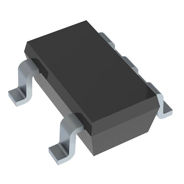
The LDO is available in fixed and adjustable output in the low
profile (1 mm max height) 5−lead TSOT23, 6−pad 1.5 mm x 1.5 mm
WDFN and in the 6−pad 2 mm x 2 mm TDFN packages.
http://onsemi.com
5
1
TSOT−23
TD SUFFIX
CASE 419AE
1
WDFN−6
MV2 SUFFIX
CASE 511BJ
PIN CONNECTIONS
1
OUT
IN
VOUT
NC/ADJ
NC
EN
GND
BYP/ADJ
WDFN−6
1
VIN
GND
EN
TSOT−23
EN
1
GND
(Top Views)
BYP/ADJ
TAB
NC
VOUT
VIN
TDFN−6
Features
•
•
•
•
•
•
•
•
•
•
•
•
•
•
•
1
TDFN−6
VP5 SUFFIX
CASE 511AH
Guaranteed 500 mA Peak Output Current
Low Dropout Voltage of 300 mV Typical at 500 mA
Stable with Ceramic Output Capacitor
External 10 nF Bypass Capacitor for Low Noise
Quick−start Feature
Under Voltage Lockout
No−load Ground Current of 55 mA Typical
Full−load Ground Current of 85 mA Typical
±1.0% Initial Accuracy (VOUT ≥ 2.0 V)
±2.0% Accuracy Over Temperature (VOUT ≥ 2.0 V)
“Zero” Current Shutdown Mode
Fold−back Current Limit
Thermal Protection
5−lead TSOT−23, 6−pad WDFN and TDFN Packages
These Devices are Pb−Free, Halogen Free/BFR Free and are RoHS
Compliant
Applications
MARKING DIAGRAMS
UMYM
US = CAT6219−125, CAT6219−250,
= CAT6219−300 Device Code
RV = CAT6219−180, CAT6219−280,
= CAT6219−285, CAT6219−330 Device Code
UM = CAT6219−ADJ Device Code
Y = Production Year (last digit)
M = Production Month: 1 − 9, A, B, C
ABYM
(TDFN)
AB = CAT6219180, CAT6219VP5 Device Code
Y = Production Year (last digit)
M = Production Month: 1 − 9, A, B, C
TM
T
S
U
V
M
• Cellular Phones
• Battery−powered Devices
• Consumer Electronics
RVYM
USYM
SM
UM
VM
(WDFN)
= CAT6219−285MV2 Device Code
= CAT6219−280MV2 Device Code
= CAT6219−330MV2 Device Code
= CAT6219−ADJMV2 Device Code
= Date Code
ORDERING INFORMATION
See detailed ordering and shipping information in the package
dimensions section on page 11 of this data sheet.
© Semiconductor Components Industries, LLC, 2012
September, 2019 − Rev. 14
1
Publication Order Number:
CAT6219/D
�CAT6219
VIN
2.3 V
to 5.5 V
OFF
CIN
VIN
1 mF
ON
VOUT
COUT
2.2 mF
VOUT
CAT6219
EN
BYP
GND
VIN
2.3 V
to 5.5 V
CBYP (Optional)
10 nF
Figure 1. Typical Application Circuit
Supply voltage input.
GND
Ground reference.
EN
Enable input (active high); a 2.5 MW pull−down
resistor is provided.
BYP
Optional bypass capacitor connection for noise
reduction and PSRR enhancing.
ADJ
Adjustable input. Feedback pin connected to
resistor divider.
VOUT
TAB
R
1) 1
R2
GND
R1
2.2 mF
ADJ
R2
EN is the enable control logic (active high) for the regulator
output. It has a 2.5 MW pull−down resistor, which assures
that if EN pin is left open, the circuit is disabled.
Function
VIN
Ǔ
EN
VOUT
COUT
Figure 2. Adjustable Output LDO
Table 1. PIN DESCRIPTIONS
Name
ǒ
VOUT
CAT6219
1 mF
OFF ON
V OUT + 1.24 V
VIN
CIN
VOUT is the LDO regulator output. A small 2.2 mF ceramic
bypass capacitor is required between the VOUT pin and
ground. For better transient response, its value can be
increased to 4.7 mF.
The capacitor should be located near the device. For the
SOT23-5 package, a continuous 500 mA output current may
turn-on the thermal protection. A 250 W internal shutdown
switch discharges the output capacitor in the no-load
condition.
GND is the ground reference for the LDO. The pin must be
connected to the ground plane on the PCB.
LDO Output Voltage.
To be connected to the ground plane on PCB
Pin Function
BYP is the reference bypass pin. An optional 0.01 mF
capacitor can be connected between BYP pin and GND to
reduce the output noise and enhance the PSRR at high
frequency.
ADJ is the adjustable input pin for the adjustable LDO. The
pin is connected to the resistor voltage divider.
VIN is the supply pin for the LDO. A small 1 mF ceramic
bypass capacitor is required between the VIN pin and ground
near the device. When using longer connections to the power
supply, CIN value can be increased without limit. The
operating input voltage range is from 2.3 V to 5.5 V.
Table 2. ABSOLUTE MAXIMUM RATINGS
Parameter
Rating
Unit
0 to 6.5
V
−0.3 to VIN + 0.3
V
+150
_C
Internally Limited (Note 1)
mW
−65 to +150
_C
260
_C
3
kV
VIN
VEN, VOUT
Junction Temperature, TJ
Power Dissipation, PD
Storage Temperature Range, TS
Lead Temperature (soldering, 5 sec.)
ESD Rating (Human Body Model)
Stresses exceeding Maximum Ratings may damage the device. Maximum Ratings are stress ratings only. Functional operation above the
Recommended Operating Conditions is not implied. Extended exposure to stresses above the Recommended Operating Conditions may affect
device reliability.
Table 3. RECOMMENDED OPERATING CONDITIONS (Note 2)
Range
Unit
VIN
2.3 to 5.5
V
VEN
0 to VIN
V
−40 to +125
_C
235
206
_C/W
Parameter
Junction Temperature Range, TJ
Package Thermal Resistance, θJA SOT23−5
Package Thermal Resistance, θJA TDFN−6
NOTE: Typical application circuit with external components is shown above.
1. The maximum allowable power dissipation at any TA (ambient temperature) is PDmax = (TJmax − TA)/qJA. Exceeding the maximum allowable
power dissipation will result in excessive die temperature, and the regulator will go into thermal shutdown.
2. The device is not guaranteed to work outside its operating rating.
http://onsemi.com
2
�CAT6219
Table 4. ELECTRICAL OPERATING CHARACTERISTICS (Note 3)
(VIN = VOUT + 1.0 V, VEN = High, IOUT = 100 mA, CIN = 1 mF, COUT = 2.2 mF, ambient temperature of 25°C (over recommended operating
conditions unless specified otherwise). Bold numbers apply for the entire junction temperature range.)
Symbol
VOUT−ACC
Parameter
Output Voltage Accuracy
TCOUT
Output Voltage Temp. Coefficient
VR−LINE
Line Regulation
Conditions
Initial accuracy for VOUT ≥ 2.0 V
(Note 6)
Min
Typ
Max
Unit
−1.0
+1.0
%
−2.0
+2.0
40
VIN = VOUT + 1.0 V to 5.5 V
−0.2
±0.1
−0.4
VR−LOAD
Load Regulation
IOUT = 100 mA to 500 mA
ppm/°C
+0.2
%/V
+0.4
1
1.5
%
2
VDROP
Dropout Voltage (Note 4)
IOUT = 500 mA
300
400
mV
500
IGND
Ground Current
IOUT = 0 mA
55
75
mA
90
IOUT = 500 mA
IGND−SD
Shutdown Ground Current
85
VEN < 0.4 V
1
mA
2
PSRR
Power Supply Rejection Ratio
f = 1 kHz, CBYP = 10 nF
64
f = 20 kHz, CBYP = 10 nF
54
dB
ISC
Output short circuit current limit
VOUT = 0 V
200
mA
TON
Turn−On Time
CBYP = 10 nF
150
ms
eN
Output Noise Voltage (Note 5)
BW = 10 Hz to 100 kHz
45
mVrms
ROUT−SH
Shutdown Switch Resistance
250
W
Enable pull−down resistor
2.5
MW
Under voltage lockout threshold
2.15
V
REN
VUVLO
ESR
COUT equivalent series resistance
VADJ
Adjustable input voltage
5
IOUT = 100 mA
1.2
VIN = 2.3 to 5.5 V
1.8
VIN = 2.3 to 5.5 V, 0°C to +125°C
junction temperature
1.6
1.24
500
mW
1.27
V
ENABLE INPUT
VHI
Logic High Level
VLO
Logic Low Level
VIN = 2.3 to 5.5 V
IEN
Enable Input Current
VEN = 0.4 V
VEN = VIN
V
0.4
V
0.15
1
mA
1.5
4
THERMAL PROTECTION
TSD
Thermal Shutdown
160
°C
THYS
Thermal Hysteresis
10
°C
3. Specification for 2.80 V output version unless specified otherwise.
4. Dropout voltage is defined as the input−to−output differential at which the output voltage drops 2% below its nominal value. During test, the
input voltage stays always above the minimum 2.3 V.
5. Specification for 1.8 V output version.
6. For VOUT < 2.0 V, the initial accuracy is ±2% and across temperature ±3%.
http://onsemi.com
3
�CAT6219
TYPICAL CHARACTERISTICS (shown for 2.80 V output option)
(VIN = 3.85 V, IOUT = 100 mA, CIN 1 mF, = COUT = 2.2 mF, CBYP = 10 nF, TA = 25°C unless otherwise specified.)
2.87
3.0
0.1 mA
500 mA
OUTPUT VOLTAGE (V)
OUTPUT VOLTAGE (V)
2.5
2.0
1.5
1.0
0.5
0
0
0.5 1.0 1.5 2.0 2.5 3.0 3.5 4.0
4.5 5.0
2.5
3.0
3.5
4.0
4.5
5.0
Figure 3. Dropout Characteristics
Figure 4. Line Regulation
5.5
2.87
OUTPUT VOLTAGE (V)
OUTPUT VOLTAGE (V)
2.83
INPUT VOLTAGE (V)
2.85
2.80
0
50
2.86
2.85
2.84
2.83
2.82
−40 −20
100 150 200 250 300 350 400 450 500
0
20
40
60
80
100
120 140
OUTPUT LOAD CURRENT (mA)
TEMPERATURE (°C)
Figure 5. Load Regulation
Figure 6. Output Voltage vs. Temperature
70
65
60
GROUND CURRENT (mA)
GROUND CURRENT (mA)
2.84
INPUT VOLTAGE (V)
2.90
50
40
30
20
10
0
2.85
2.82
5.5
2.95
2.75
2.86
0
61
57
53
49
45
−40 −20
0.5 1.0 1.5 2.0 2.5 3.0 3.5 4.0 4.5 5.0 5.5
0
20
40
60
80
100
120 140
INPUT VOLTAGE (V)
TEMPERATURE (°C)
Figure 7. Ground Current vs. Input Voltage
Figure 8. Ground Current vs. Temperature
http://onsemi.com
4
�CAT6219
TYPICAL CHARACTERISTICS (shown for 2.80 V output option)
(VIN = 3.85 V, IOUT = 100 mA, CIN 1 mF, = COUT = 2.2 mF, CBYP = 10 nF, TA = 25°C unless otherwise specified.)
GROUND CURRENT (mA)
100
90
80
70
60
50
0
100 150 200 250 300 350 400 450 500
50
OUTPUT LOAD CURRENT (mA)
Figure 9. Ground Current vs. Load Current
400
450
DROPOUT VOLTAGE (mV)
500 mA DROPOUT VOLTAGE (mV)
500
400
350
300
250
350
300
250
200
150
100
50
200
−40 −20
0
20
40
60
80
100
120
0
140
0
100 150 200 250 300 350 400 450 500
50
TEMPERATURE (°C)
OUTPUT LOAD CURRENT (mA)
Figure 10. Dropout vs. Temperature
(500 mA Load)
Figure 11. Dropout vs. Load Current
1.6
80
CBYP = 10 nF
60
1.2
PSRR (dB)
ENABLE THRESHOLD (V)
70
0.8
CBYP = 0
50
40
30
20
0.4
10
0
2.0
2.5
3.0
3.5
4.0
4.5
5.0
0
5.5
1.0E+01
1.0E+02
1.0E+03
1.0E+04
1.0E+05
INPUT VOLTAGE (V)
FREQUENCY (Hz)
Figure 12. Enable Threshold vs. Input Voltage
Figure 13. PSRR vs. Frequency (10 mA Load)
http://onsemi.com
5
�CAT6219
TRANSIENT CHARACTERISTICS (shown for 2.80 V output option)
(VIN = 3.85 V, IOUT = 100 mA, CIN 1 mF, = COUT = 2.2 mF, CBYP = 10 nF, TA = 25°C unless otherwise specified.)
Figure 14. Enable Turn−on (100 mA Load)
Figure 15. Enable Turn−off (100 mA Load)
Figure 16. Enable Turn−on (500 mA Load)
Figure 17. Enable Turn−off (500 mA Load)
Figure 18. Line Transient Response
(3.85 V to 4.85 V)
Figure 19. Load Transient Response
(0.1 mA to 500 mA)
http://onsemi.com
6
�CAT6219
VOUT
VIN
ENABLE
Enable
Logic
VOUT
VIN
+
+
−
−
VREF +
−
BYPASS
ENABLE
GND
Enable
Logic
VREF +
−
GND
Figure 20. Block Diagram − Fixed Voltage
Figure 21. Block Diagram − Adjustable Voltage
http://onsemi.com
7
ADJ
�CAT6219
PACKAGE DIMENSIONS
TSOT−23, 5 LEAD
CASE 419AE−01
ISSUE O
SYMBOL
D
MIN
NOM
A1
0.01
0.05
0.10
A2
0.80
0.87
0.90
b
0.30
c
0.12
A
e
E1
1.00
0.45
0.15
D
2.90 BSC
E
2.80 BSC
E1
1.60 BSC
E
MAX
e
0.20
0.95 TYP
L
0.30
0.40
L1
0.60 REF
L2
0.25 BSC
0º
θ
0.50
8º
TOP VIEW
A2 A
b
q
L
A1
c
L1
SIDE VIEW
END VIEW
Notes:
(1) All dimensions are in millimeters. Angles in degrees.
(2) Complies with JEDEC MO-193.
http://onsemi.com
8
L2
�CAT6219
PACKAGE DIMENSIONS
TDFN6, 2x2
CASE 511AH−01
ISSUE A
D
A
DETAIL A
DAP SIZE 1.8 x 1.2
E2
PIN#1
IDENTIFICATION
PIN# 1 INDEX AREA
A1
TOP VIEW
SIDE VIEW
SYMBOL
MIN
NOM
MAX
A
0.70
0.75
0.80
A1
0.00
0.02
0.05
A3
BOTTOM VIEW
e
0.25
0.30
0.35
D
1.90
2.00
2.10
D2
1.50
1.60
1.70
E
1.90
2.00
2.10
E2
0.90
1.00
1.10
e
L
b
0.20 REF
b
L
D2
DETAIL A
A
0.65 TYP
0.15
0.25
0.35
A1
Notes:
(1) All dimensions are in millimeters.
(2) Complies with JEDEC standard MO-229.
http://onsemi.com
9
FRONT VIEW
A3
�CAT6219
PACKAGE DIMENSIONS
WDFN6 1.5x1.5, 0.5P
CASE 511BJ−01
ISSUE B
D
L
A
B
NOTES:
1. DIMENSIONING AND TOLERANCING PER
ASME Y14.5M, 1994.
2. CONTROLLING DIMENSION: MILLIMETERS.
3. DIMENSION b APPLIES TO PLATED
TERMINAL AND IS MEASURED BETWEEN
0.15 AND 0.30mm FROM TERMINAL TIP.
4. COPLANARITY APPLIES TO THE EXPOSED
PAD AS WELL AS THE TERMINALS.
L1
DETAIL A
ÍÍÍÍ
ÍÍÍÍ
ÍÍÍÍ
ALTERNATE TERMINAL
CONSTRUCTIONS
E
PIN ONE
REFERENCE
ÉÉÉ
ÉÉÉ
EXPOSED Cu
0.10 C
2X
2X
0.10 C
0.05 C
TOP VIEW
DETAIL B
A3
MOLD CMPD
ÉÉ
ÉÉ
ÇÇ
A3
A1
DETAIL B
ALTERNATE
CONSTRUCTIONS
0.05 C
1
A1
C
SIDE VIEW
DETAIL A
e
1
SEATING
PLANE
X MG
G
X
= Specific Device Code
M = Date Code
G
= Pb−Free Package
(*Note: Microdot may be in either location)
5X
L
3
MILLIMETERS
MIN
MAX
0.70
0.80
0.00
0.05
0.20 REF
0.20
0.30
1.50 BSC
1.50 BSC
0.50 BSC
0.40
0.60
--0.15
0.50
0.70
GENERIC
MARKING DIAGRAM*
A
NOTE 4
DIM
A
A1
A3
b
D
E
e
L
L1
L2
L2
*This information is generic. Please refer to
device data sheet for actual part marking.
Pb−Free indicator, “G” or microdot “ G”,
may or may not be present.
6
4
6X
RECOMMENDED
MOUNTING FOOTPRINT*
b
0.10 C A
BOTTOM VIEW
0.05 C
B
6X
NOTE 3
0.35
5X
0.73
1.80
0.83
0.50
PITCH
DIMENSIONS: MILLIMETERS
*For additional information on our Pb−Free strategy and soldering
details, please download the ON Semiconductor Soldering and
Mounting Techniques Reference Manual, SOLDERRM/D.
http://onsemi.com
10
�CAT6219
ORDERING INFORMATION (Notes 7 − 9)
Device Order Number
Specific
Device
Marking
Package
Type
VOUT
Voltage (V)
CAT6219−125TDGT3
US
1.25
CAT6219−180TDGT3
RV
1.80
CAT6219−250TDGT3
US
2.50
CAT6219−280TDGT3
RV
CAT6219−285TDGT3
RV
CAT6219−300TDGT3
US
3.00
CAT6219−330TDGT3
RV
3.30
CAT6219ADJTD−GT3
UM
Adjustable
CAT6219ADJVP5GT4
AF
Lead Finish
2.80
TSOT−23−5
Shipping (Note 10)
Tape & Reel, 3,000 Units / Reel
2.85
NiPdAu
Adjustable
TDFN−6
(2.0 x 2.0)
CAT6219180VP5GT4
AB
CAT6219VP5330GT4
AB
1.80
3.30
CAT6219−280MV2T3
S
2.80
CAT6219−285MV2T3
T
CAT6219−330MV2T3
U
CAT6219ADJMV2−T3
V
2.85
WDFN−6
(1.5 x 1.5)
3.30
Tape & Reel, 4,000 Units / Reel
Tape & Reel, 3,000 Units / Reel
Adjustable
7. All packages are RoHS−compliant (Lead−free, Halogen−free).
8. The standard lead finish is NiPdAu pre−plated (PPF) lead frames.
9. For other voltage options, please contact your nearest ON Semiconductor Sales office.
10. For information on tape and reel specifications, including part orientation and tape sizes, please refer to our Tape and Reel Packaging
Specifications Brochure, BRD8011/D.
11. For detailed information and a breakdown of device nomenclature and numbering systems, please see the ON Semiconductor Device
Nomenclature document, TND310/D, available at www.onsemi.com
ON Semiconductor and
are registered trademarks of Semiconductor Components Industries, LLC (SCILLC). SCILLC owns the rights to a number of patents, trademarks,
copyrights, trade secrets, and other intellectual property. A listing of SCILLC’s product/patent coverage may be accessed at www.onsemi.com/site/pdf/Patent−Marking.pdf. SCILLC
reserves the right to make changes without further notice to any products herein. SCILLC makes no warranty, representation or guarantee regarding the suitability of its products for any
particular purpose, nor does SCILLC assume any liability arising out of the application or use of any product or circuit, and specifically disclaims any and all liability, including without
limitation special, consequential or incidental damages. “Typical” parameters which may be provided in SCILLC data sheets and/or specifications can and do vary in different applications
and actual performance may vary over time. All operating parameters, including “Typicals” must be validated for each customer application by customer’s technical experts. SCILLC
does not convey any license under its patent rights nor the rights of others. SCILLC products are not designed, intended, or authorized for use as components in systems intended for
surgical implant into the body, or other applications intended to support or sustain life, or for any other application in which the failure of the SCILLC product could create a situation where
personal injury or death may occur. Should Buyer purchase or use SCILLC products for any such unintended or unauthorized application, Buyer shall indemnify and hold SCILLC and
its officers, employees, subsidiaries, affiliates, and distributors harmless against all claims, costs, damages, and expenses, and reasonable attorney fees arising out of, directly or indirectly,
any claim of personal injury or death associated with such unintended or unauthorized use, even if such claim alleges that SCILLC was negligent regarding the design or manufacture
of the part. SCILLC is an Equal Opportunity/Affirmative Action Employer. This literature is subject to all applicable copyright laws and is not for resale in any manner.
PUBLICATION ORDERING INFORMATION
LITERATURE FULFILLMENT:
Literature Distribution Center for ON Semiconductor
P.O. Box 5163, Denver, Colorado 80217 USA
Phone: 303−675−2175 or 800−344−3860 Toll Free USA/Canada
Fax: 303−675−2176 or 800−344−3867 Toll Free USA/Canada
Email: orderlit@onsemi.com
N. American Technical Support: 800−282−9855 Toll Free
USA/Canada
Europe, Middle East and Africa Technical Support:
Phone: 421 33 790 2910
Japan Customer Focus Center
Phone: 81−3−5817−1050
http://onsemi.com
11
ON Semiconductor Website: www.onsemi.com
Order Literature: http://www.onsemi.com/orderlit
For additional information, please contact your local
Sales Representative
CAT6219/D
�


 工商网监
湘ICP备2023018690号
工商网监
湘ICP备2023018690号
