ON Semiconductor
Is Now
To learn more about onsemi™, please visit our website at
www.onsemi.com
onsemi and and other names, marks, and brands are registered and/or common law trademarks of Semiconductor Components Industries, LLC dba “onsemi” or its affiliates and/or
subsidiaries in the United States and/or other countries. onsemi owns the rights to a number of patents, trademarks, copyrights, trade secrets, and other intellectual property. A listing of onsemi
product/patent coverage may be accessed at www.onsemi.com/site/pdf/Patent-Marking.pdf. onsemi reserves the right to make changes at any time to any products or information herein, without
notice. The information herein is provided “as-is” and onsemi makes no warranty, representation or guarantee regarding the accuracy of the information, product features, availability, functionality,
or suitability of its products for any particular purpose, nor does onsemi assume any liability arising out of the application or use of any product or circuit, and specifically disclaims any and all
liability, including without limitation special, consequential or incidental damages. Buyer is responsible for its products and applications using onsemi products, including compliance with all laws,
regulations and safety requirements or standards, regardless of any support or applications information provided by onsemi. “Typical” parameters which may be provided in onsemi data sheets and/
or specifications can and do vary in different applications and actual performance may vary over time. All operating parameters, including “Typicals” must be validated for each customer application
by customer’s technical experts. onsemi does not convey any license under any of its intellectual property rights nor the rights of others. onsemi products are not designed, intended, or authorized
for use as a critical component in life support systems or any FDA Class 3 medical devices or medical devices with a same or similar classification in a foreign jurisdiction or any devices intended for
implantation in the human body. Should Buyer purchase or use onsemi products for any such unintended or unauthorized application, Buyer shall indemnify and hold onsemi and its officers, employees,
subsidiaries, affiliates, and distributors harmless against all claims, costs, damages, and expenses, and reasonable attorney fees arising out of, directly or indirectly, any claim of personal injury or death
associated with such unintended or unauthorized use, even if such claim alleges that onsemi was negligent regarding the design or manufacture of the part. onsemi is an Equal Opportunity/Affirmative
Action Employer. This literature is subject to all applicable copyright laws and is not for resale in any manner. Other names and brands may be claimed as the property of others.
�CAT8900
Precision Analog Voltage
References
The CAT8900 is a high precision voltage reference providing very
accurate voltage regulation with low supply current consumption.
CAT8900 is ideal for use in battery powered systems where
operating current needs to be minimized and there can be a great
variation in supply voltages. It will source or sink up to 10 mA of load
current, and can for most applications, forgo the use of an output
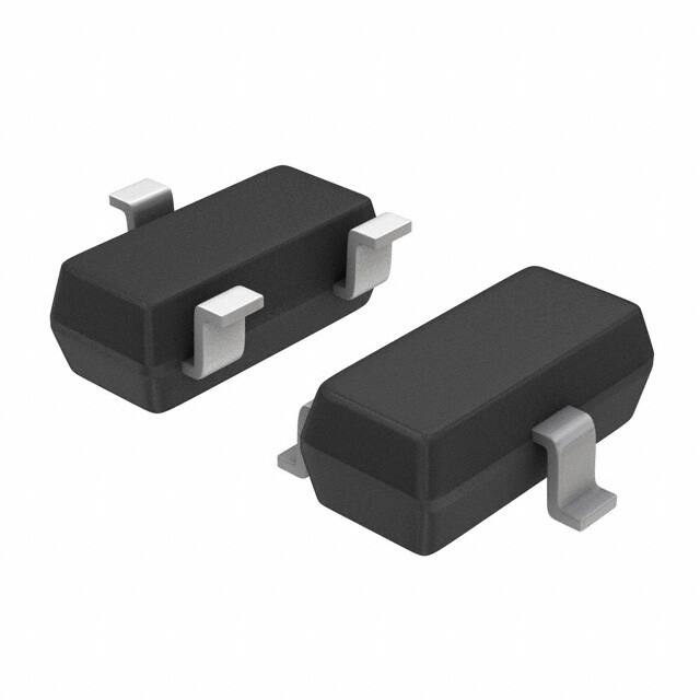
bypass capacitor. The device is supplied in a space saving three
terminal SOT−23 package.
http://onsemi.com
Features
SOT23−3
TP, TB SUFFIX
CASE 527AG
• Reference Voltages:
•
•
•
•
•
1.024 V, 1.200 V, 1.250 V, 1.800 V,
2.048 V, 2.500 V, 2.600 V,
3.000 V, 3.300 V
Low Supply Current: 450 nA (Typical)
Initial Accuracy:
Class B: ± 1.0 mV
Class C: ± 2.5 mV
Class D: ± 5.0 mV
Drift Performance: 50 ppm/°C
SOT−23 3−Lead Package
This Device is Pb−Free, Halogen Free/BFR Free, and RoHS
Compliant
MARKING DIAGRAM
3
S3YM
S3 = Specific Device Code
Y = Production Year
= (Last Digit)
M = Production Month
= (1 − 9, A, B, C)
Typical Applications
•
•
•
•
•
2
1
Battery Powered Systems
A/D and D/A Converters
Precision Regulator Systems
Power Supplies
Portable Medical Equipment
PIN CONNECTIONS
1
VIN
3
GND
2
VIN
VIN
C
0.1 mF
VOUT
VOUT
VOUT
(Top View)
CAT8900
PIN FUNCTIONS
GND
Figure 1. Application Circuit
Pin No.
Pin Name
Function
1
VIN
2
VOUT
Output Voltage
3
GND
Ground
Supply Voltage Input
ORDERING INFORMATION
See detailed ordering and shipping information in the package
dimensions section on page 2 of this data sheet.
© Semiconductor Components Industries, LLC, 2011
January, 2020 − Rev. 8
1
Publication Order Number:
CAT8900/D
�CAT8900
Table 1. ORDERING INFORMATION
Orderable Part Number
Initial Accuracy
(±mV)
Initial Accuracy
(%)
CAT8900B102TBGT3
1.0
0.10%
CAT8900C102TBGT3
2.5
0.24%
CAT8900D102TBGT3
5.0
0.49%
CAT8900B120TBGT3
1.0
0.08%
CAT8900C120TBGT3
2.5
0.21%
CAT8900D120TBGT3
5.0
0.42%
CAT8900B125TBGT3
1.0
0.08%
CAT8900C125TBGT3
2.5
0.20%
CAT8900D125TBGT3
5.0
0.40%
CAT8900B180TBGT3
1.0
0.06%
CAT8900C180TBGT3
2.5
0.14%
CAT8900D180TBGT3
5.0
0.28%
CAT8900B204TBGT3
1.0
0.05%
CAT8900C204TBGT3
2.5
0.12%
CAT8900D204TBGT3
5.0
0.24%
CAT8900B250TBGT3
1.0
0.04%
CAT8900C250TBGT3
2.5
0.10%
CAT8900D250TBGT3
5.0
0.20%
CAT8900B260TBGT3
1.0
0.04%
CAT8900C260TBGT3
2.5
0.10%
CAT8900D260TBGT3
5.0
0.19%
CAT8900B300TBGT3
1.0
0.03%
CAT8900C300TBGT3
2.5
0.08%
CAT8900D300TBGT3
5.0
0.17%
CAT8900B330TBGT3
1.0
0.03%
CAT8900C330TBGT3
2.5
0.08%
CAT8900D330TBGT3
5.0
0.15%
VOUT Voltage (V)
(Note 1)
Package
Shipping†
SOT−23
3,000
1.024
1.200
1.250
1.800
2.048
2.500
2.600
3.000
3.300
1. Contact factory for availability of these and other custom voltages.
†For information on tape and reel specifications, including part orientation and tape sizes, please refer to our Tape and Reel Packaging
Specifications Brochure, BRD8011/D.
http://onsemi.com
2
�CAT8900
Table 2. ABSOLUTE MAXIMUM RATINGS (Note 2)
Value
Unit
6.5
V
Storage Temperature Range
−55 to +125
_C
Junction Temperature Range
+150
_C
Rating
VIN
Stresses exceeding Maximum Ratings may damage the device. Maximum Ratings are stress ratings only. Functional operation above the
Recommended Operating Conditions is not implied. Extended exposure to stresses above the Recommended Operating Conditions may affect
device reliability.
2. Maximum terminal current is bounded by the maximum current handling of the switches, maximum power dissipation of the package.
Table 3. RECOMMENDED OPERATING CONDITIONS
Rating
Temperature Range
Value
Unit
−40 to +85
_C
Table 4. ELECTRICAL CHARACTERISTICS
VIN = 3.0 V, IOUT = 0 mA, COUT = 0.001 mF, −40_C to +85_C unless specified otherwise.
Parameter
Test Conditions
Symbol
Min
VOUT
Typ
Max
Output Voltage
CAT8900x102
CAT8900x120
CAT8900x125
CAT8900x180
CAT8900x204
CAT8900x250
CAT8900x260
CAT8900x300 (VIN = 5.0 V)
CAT8900x330 (VIN = 5.0 V)
Initial Accuracy
Grade B (TA = 25°C)
−1.0
+1.0
Grade C (TA = 25°C)
−2.5
+2.5
Grade D (TA = 25°C)
−5.0
+5.0
Output Voltage Noise (Note 3)
f = 0.1 Hz to 10 Hz
Output Voltage Temperature Drift
−40°C to 85°C
Thermal Hysteresis (Note 3)
Line Regulation
Dropout Voltage
VIN = 3.0 V, CAT8900x250
Load Regulation Sourcing
0 mA < ILOAD < 10 mA; VIN = 3 V
Sinking
−10 mA < ILOAD < 0 mA;
VIN = 3 V
Long Term Stability (Note 3)
TA = 25°C; first 1000 hours
1.024
1.200
1.250
1.800
2.048
2.500
2.600
3.000
3.300
V
50
DVOUT ÷ DT
20
ΔTA = 125°C
DVOUT ÷ DTA
100
2.7 V < VIN < 5.5 V
DVOUT ÷ DVIN
TA = 25°C
VOUT pin shorted to GND
VOUT pin shorted to VIN
Turn−on Settling Time
0.1% @ VIN = 3 V; CL = 0 pF
mVp−p
ppm/°C
30
100
mV/V
VDO
1.0
2.5
mV
DVOUT ÷ DILOAD
100
250
mV/mA
150
350
mV/mA
ILOAD
Short Circuit Current (Note 3)
Sourcing
Sinking
mV
50
ppm
50
DVOUT ÷ Dt
Output Current
Unit
−10
ppm
+10
ISC
mA
mA
40
20
60
40
2
ms
POWER SUPPLY
Input Voltage
IL = 0 mA
VIN
Supply current
IIN
3. Guaranteed by design.
http://onsemi.com
3
2.7
450
5.5
V
800
nA
�CAT8900
TYPICAL CHARACTERISTICS
700
650
650
600
SUPPLY CURRENT (nA)
SUPPLY CURRENT (nA)
(VIN = 3.0 V, IOUT = 0 mA, ambient temperature of 25°C, unless specified otherwise.)
Unit 1
600
550
Unit 2
500
Unit 3
450
400
350
2.5
3.0
3.5
4.0
4.5
5.0
+25°C
450
−40°C
400
2.5
3.0
4.5
5.0
5.5
Figure 2. Supply Current vs. Input Voltage
Figure 3. Supply Current vs. Input Voltage
Over Temperature
50
Unit 1
1.2500
Unit 2
Unit 3
1.2499
2.5
3.0
3.5
4.0
5.0
4.5
5.5
−40°C
+85°C
25
+25°C
0
−25
2.5
3.0
INPUT VOLTAGE (V)
2.0
4.0
4.5
5.0
5.5
Figure 5. Line Regulation Over Temperature
Normalized
1.2508
+85°C
1.2506
1.5
OUTPUT VOLTAGE (V)
+25°C
1.0
−40°C
0
−0.5
−1.0
−1.5
−10
3.5
INPUT VOLTAGE (V)
Figure 4. Line Regulation
OUTPUT VOLTAGE CHANGE (mV)
4.0
INPUT VOLTAGE (V)
1.2501
0.5
3.5
INPUT VOLTAGE (V)
OUTPUT VOLTAGE CHANGE (mV)
OUTPUT VOLTAGE (V)
+85°C
500
350
5.5
1.2502
1.2498
550
SINKING
−5
SOURCING
0
5
1.2504
1.2502
1.2500
1.2498
1.2496
Unit 2
1.2494
Unit 1
1.2492
−40
10
Unit 3
−15
10
35
60
OUTPUT CURRENT (mA)
TEMPERATURE (°C)
Figure 6. Load Regulation Over Temperature
Figure 7. Output Voltage vs. Temperature
Normalized
http://onsemi.com
4
85
�CAT8900
TYPICAL CHARACTERISTICS
100 mV / DIV
100 mV / DIV
(VIN = 3.0 V, IOUT = 0 mA, ambient temperature of 25°C, unless specified otherwise.)
1 ms / DIV
Figure 8. Line Transient Response
Figure 9. Line Transient Response with
Capacitive Load
50 mV / DIV
200 mV / DIV
1 ms / DIV
500 ms / DIV
500 ms / DIV
Figure 10. Load Transient Response
Figure 11. Load Transient Response
160
140
1 nF Load
120
−20
10 nF Load
100
80
60
100 nF Load
−30
−60
−70
−80
10
100
1k
10 k
100 k
10 nF Load
−50
20
1
1 nF Load
−40
40
0
No Load
−10
PSRR (dB)
OUTPUT IMPEDANCE (W)
0
No Load
−90
100 nF Load
1
10
100
1k
10 k
100 k
1M
FREQUENCY (Hz)
FREQUENCY (Hz)
Figure 12. Output Impedance vs. Frequency
Figure 13. Power Supply Rejection Ratio vs.
Frequency
http://onsemi.com
5
�CAT8900
TYPICAL CHARACTERISTICS
10 mV / DIV
500 mV / DIV
(VIN = 3.0 V, IOUT = 0 mA, ambient temperature of 25°C, unless specified otherwise.)
1 ms / DIV
10 s / DIV
Figure 14. Turn−On Time
Figure 15. Output Noise
http://onsemi.com
6
�CAT8900
PACKAGE DIMENSIONS
SOT−23, 3 Lead
CASE 527AG−01
ISSUE O
D
SYMBOL
MIN
A
0.89
1.12
A1
0.013
0.10
b
0.37
0.50
c
0.085
0.18
D
2.80
3.04
E
2.10
2.64
E1
1.20
1.40
3
E1
1
E
2
e
MAX
e
0.95 BSC
e1
1.90 BSC
L
0.40 REF
e1
L1
TOP VIEW
θ
A
NOM
0.54 REF
0°
8°
q
b
L1
A1
SIDE VIEW
L
c
END VIEW
Notes:
(1) All dimensions are in millimeters. Angles in degrees.
(2) Complies with JEDEC TO-236.
ON Semiconductor and
are registered trademarks of Semiconductor Components Industries, LLC (SCILLC). SCILLC reserves the right to make changes without further notice
to any products herein. SCILLC makes no warranty, representation or guarantee regarding the suitability of its products for any particular purpose, nor does SCILLC assume any liability
arising out of the application or use of any product or circuit, and specifically disclaims any and all liability, including without limitation special, consequential or incidental damages.
“Typical” parameters which may be provided in SCILLC data sheets and/or specifications can and do vary in different applications and actual performance may vary over time. All
operating parameters, including “Typicals” must be validated for each customer application by customer’s technical experts. SCILLC does not convey any license under its patent rights
nor the rights of others. SCILLC products are not designed, intended, or authorized for use as components in systems intended for surgical implant into the body, or other applications
intended to support or sustain life, or for any other application in which the failure of the SCILLC product could create a situation where personal injury or death may occur. Should
Buyer purchase or use SCILLC products for any such unintended or unauthorized application, Buyer shall indemnify and hold SCILLC and its officers, employees, subsidiaries, affiliates,
and distributors harmless against all claims, costs, damages, and expenses, and reasonable attorney fees arising out of, directly or indirectly, any claim of personal injury or death
associated with such unintended or unauthorized use, even if such claim alleges that SCILLC was negligent regarding the design or manufacture of the part. SCILLC is an Equal
Opportunity/Affirmative Action Employer. This literature is subject to all applicable copyright laws and is not for resale in any manner.
PUBLICATION ORDERING INFORMATION
LITERATURE FULFILLMENT:
Literature Distribution Center for ON Semiconductor
P.O. Box 5163, Denver, Colorado 80217 USA
Phone: 303−675−2175 or 800−344−3860 Toll Free USA/Canada
Fax: 303−675−2176 or 800−344−3867 Toll Free USA/Canada
Email: orderlit@onsemi.com
N. American Technical Support: 800−282−9855 Toll Free
USA/Canada
Europe, Middle East and Africa Technical Support:
Phone: 421 33 790 2910
Japan Customer Focus Center
Phone: 81−3−5773−3850
http://onsemi.com
7
ON Semiconductor Website: www.onsemi.com
Order Literature: http://www.onsemi.com/orderlit
For additional information, please contact your local
Sales Representative
CAT8900/D
�


 工商网监
湘ICP备2023018690号
工商网监
湘ICP备2023018690号
