CAT9532
I/O Port Expander, I2C /
SMBus, 16-Bit, with LED
Dimming
Description
The CAT9532 is a CMOS device that provides 16−bit parallel
input/output port expander optimized for LED dimming control. The
CAT9532 outputs can drive directly 16 LEDs in parallel. Each
individual LED may be turned ON, OFF, or blinking at one of two
programmable rates. The device provides a simple solution for
dimming LEDs in 256 brightness steps for backlight and color mixing
applications. The CAT9532 is suitable in I2C and SMBus compatible
applications where it is necessary to limit the bus traffic or free−up the
bus master’s timer.
The CAT9532 contains an internal oscillator and two PWM signals
that drive the LED outputs. The user can program the period and duty
cycle for each individual PWM signal. After the initial set−up
command to program the Blink Rate 1 and Blink Rate 2 (frequency
and duty cycle), only one command from the bus master is required to
turn each individual open drain output ON, OFF, or cycle at Blink
Rate 1 or Blink Rate 2. Each open drain LED output can provide a
maximum output current of 25 mA. The total current sunk by all I/Os
must not exceed 400 mA.
www.onsemi.com
TSSOP−24
Y SUFFIX
CASE 948AR
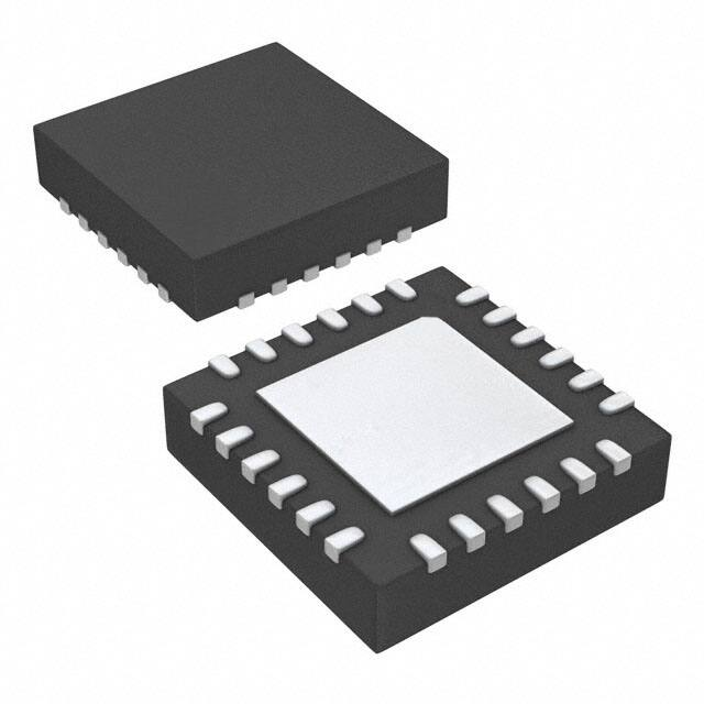
TQFN−24
HV6 SUFFIX
CASE 510AG
ORDERING INFORMATION
Features
•
•
•
•
•
•
•
•
•
•
•
16 LED Drivers with Dimming Control
256 Brightness Steps
16 Open Drain Outputs Drive 25 mA Each
2 Selectable Programmable Blink Rates:
– Frequency: 0.593 Hz to 152 Hz
– Duty Cycle: 0% to 99.6%
I/Os can be Used as GPIOs
400 kHz I2C Bus Compatible
2.3 V to 5.5 V Operation
5 V Tolerant I/Os
Active Low Reset Input
24−Lead TSSOP and 24−pad TQFN (4 x 4 mm) Packages
These Devices are Pb−Free, Halogen Free/BFR Free and are RoHS
Compliant
See detailed ordering and shipping information in the package
dimensions section on page 14 of this data sheet.
Applications
•
•
•
•
•
Backlighting
RGB Color Mixing
Sensors Control
Power Switches, Push−buttons
Alarm Systems
© Semiconductor Components Industries, LLC, 2016
October, 2016 − Rev. 5
1
Publication Order Number:
CAT9532/D
�CAT9532
MARKING DIAGRAMS
LAAC
AXXX
YMCC
AB
CAT9532YI
3YMXXX
TQFN (HV6)
A0
SCL
SDA
A2
Y
M
CC
VCC
A
= Assembly Location
B
= Product Revision (Fixed as “B”)
CAT9532Y = Device Code
I
= Temperature Range
3
= Matte-Tin Lead Finish
Y
= Production Year (Last Digit)
M
= Production Month (1−9, O, N, D)
XXX
= Last Three Digits of
= Assembly Lot Number
= Device Code
= Assembly Location
= Last Three Digits of
= Assembly Lot Number
= Production Year (Last Digit)
= Production Month (1−9, O, N, D)
= Country Code
= TH = Thailand
= MY = Malaysia
A0
LAAC
A
XXX
A1
TSSOP (Y)
VCC
1
A1
SDA
A2
LED0
RESET
LED0
SCL
RESET
LED1
LED15
LED1
LED15
LED2
LED14
LED2
LED14
LED3
LED13
LED3
LED13
LED4
LED12
LED4
LED12
LED5
LED11
LED5
LED11
LED6
LED10
LED7
LED9
VSS
LED8
TSSOP (Y)
(Top View)
TQFN (HV6)
(Top View)
Figure 1. Pin Configurations
5V
5V
RS0
3 x 10 kW
SDA
SDA
SCL
SCL
RS11
VCC
RESET
RESET
I2C/SMBus
RS1
LED0
LED1
CAT9532
Master
LED11
LED12
A2
A1
A0
VSS
GPIOs
LED15
Figure 2. Typical Application Circuit
www.onsemi.com
2
LED10
LED9
LED8
VSS
LED7
LED6
1
�CAT9532
Table 1. PIN DESCRIPTION
TSSOP
TQFN
Pin Name
1
22
A0
Address Input 0
2
23
A1
Address Input 1
3
24
A2
Address Input 2
4−11
1−8
LED0 − LED7
12
9
VSS
13−20
10−17
LED8 − LED15
21
18
RESET
Reset Input
22
19
SCL
Serial Clock
23
20
SDA
Serial Data
24
21
VCC
Power Supply
A2
A1
Function
LED Driver Output 0 to 7, I/O Port 0 to 7
Ground
LED Driver Output 8 to 15, I/O Port 8 to 15
A0
VCC
POWER ON
RESET
INPUT
REGISTER
RESET
INPUT
FILTERS
SCL
SDA
LED SELECT (LSx)
REGISTER
I2C BUS
CONTROL
LEDx
PRESCALER 0
REGISTER
PWM 0
REGISTER
BLINK 0
PRESCALER 1
REGISTER
PWM 1
REGISTER
BLINK 1
OSCILLATOR
VSS
CONTROL
LOGIC
CAT9532
Note: Only one I/O is shown for clarity
Figure 3. Block Diagram
Table 2. ABSOLUTE MAXIMUM RATINGS
Parameters
Ratings
Units
VCC with Respect to Ground
−0.3 to +7.0
V
Voltage on Any Pin with Respect to Ground
−0.3 to +5.5
V
DC Current on I/Os
±25
mA
Supply Current
400
mA
Package Power Dissipation Capability (TA = 25°C)
1.0
W
Junction Temperature
+150
°C
Storage Temperature
−65 to +150
°C
300
°C
−40 to +85
°C
Lead Soldering Temperature (10 seconds)
Operating Ambient Temperature
Stresses exceeding those listed in the Maximum Ratings table may damage the device. If any of these limits are exceeded, device functionality
should not be assumed, damage may occur and reliability may be affected.
www.onsemi.com
3
�CAT9532
Table 3. D.C. OPERATING CHARACTERISTICS (VCC = 2.3 to 5.5 V, VSS = 0 V; TA = −40°C to +85°C, unless otherwise specified)
Symbol
Parameter
Conditions
Min
Typ
Max
Unit
2.3
−
5.5
V
SUPPLIES
VCC
Supply Voltage
ICC
Supply Current
Operating mode; VCC = 5.5 V; no load;
fSCL = 100 kHz
−
250
550
mA
Istb
Standby Current
Standby mode; VCC = 5.5 V; no load;
VI = VSS or VCC, fSCL = 0 kHz
−
2.1
5.0
mA
Additional Standby Current
Standby mode; VCC = 5.5 V; every
LED I/O = VIN = 4.3 V, fSCL = 0 kHz
−
−
2
mA
Power−on Reset Voltage
VCC = 3.3 V, No load;
VI = VCC or VSS
−
1.5
2.2
V
ΔIstb
VPOR (Note 1)
SCL, SDA
VIL (Note 2)
Low Level Input Voltage
−0.3
−
0.3 VCC
V
VIH (Note 2)
High Level Input Voltage
0.7 VCC
−
5.5
V
IOL
Low Level Output Current
VOL = 0.4 V
3
−
−
mA
IIL
Leakage Current
VI = VCC = VSS
−1
−
+1
mA
CI (Note 3)
Input Capacitance
VI = VSS
−
−
6
pF
CO (Note 3)
Output Capacitance
VO = VSS
−
−
8
pF
A0, A1, A2
VIL (Note 2)
Low Level Input Voltage
−0.3
−
0.8
V
VIH (Note 2)
High Level Input Voltage
2.0
−
5.5
V
Input Leakage Current
−1
−
1
mA
−0.3
−
0.8
V
IIL
I/Os
VIL (Note 2)
Low Level Input Voltage
VIH (Note 2)
High Level Input Voltage
IOL (Note 4)
Low Level Output Current
IIL
CI/O (Note 3)
Input Leakage Current
2.0
−
5.5
V
VOL = 0.4 V; VCC = 2.3 V
9
−
−
mA
VOL = 0.4 V; VCC = 3.0 V
12
−
−
VOL = 0.4 V; VCC = 5.0 V
15
−
−
VOL = 0.7 V; VCC = 2.3 V
15
−
−
VOL = 0.7 V; VCC = 3.0 V
20
−
−
VOL = 0.7 V; VCC = 5.0 V
25
−
−
VCC = 3.6 V; VI = VSS or VCC
−1
−
1
mA
−
−
8
pF
Input/Output Capacitance
RESET
VIL (Note 2)
Low Level Input Voltage
−0.3
−
0.2 VCC
V
VIH (Note 2)
High Level Input Voltage
0.7 VCC
−
5.5
V
−1
−
1
mA
IIL
Input Leakage Current
VI = VCC or VSS
Product parametric performance is indicated in the Electrical Characteristics for the listed test conditions, unless otherwise noted. Product
performance may not be indicated by the Electrical Characteristics if operated under different conditions.
1. VCC must be lowered to 0.2 V in order to reset the device.
2. VIL min and VIH max are reference values only and are not tested.
3. This parameter is characterized initially and after a design or process change that affects the parameter. Not 100% tested.
4. The output current must be limited to a maximum 25 mA per each I/O; the total current sunk by all I/O must be limited to 400 mA.
www.onsemi.com
4
�CAT9532
Table 4. A.C. CHARACTERISTICS (VCC = 2.3 V to 5.5 V, TA = −40°C to +85°C, unless otherwise specified) (Note 5)
Standard I2C
Min
Parameter
Symbol
FSCL
Max
Clock Frequency
tHD:STA
Fast I2C
Min
100
START Condition Hold Time
Max
Units
400
kHz
4
0.6
ms
tLOW
Low Period of SCL Clock
4.7
1.3
ms
tHIGH
High Period of SCL Clock
4
0.6
ms
4.7
0.6
ms
tSU:STA
START Condition Setup Time
tHD:DAT
Data In Hold Time
0
0
ms
tSU:DAT
Data In Setup Time
250
100
ns
tR (Note 6)
SDA and SCL Rise Time
tF (Note 6)
1000
SDA and SCL Fall Time
tSU:STO
300
STOP Condition Setup Time
tBUF (Note 6)
Bus Free Time Between STOP and START
tAA
SCL Low to Data Out Valid
tDH
Data Out Hold Time
Ti (Note 6)
300
ns
300
ns
4
0.6
ms
4.7
1.3
ms
3.5
100
Noise Pulse Filtered at SCL and SDA Inputs
0.9
50
50
ms
ns
50
ns
PORT TIMING
tPV
Output Data Valid
200
ns
tPS
Input Data Setup Time
100
ns
tPH
Input Data Hold Time
1
ms
Reset Pulse Width
20
ns
0
ns
400
ns
RESET
tW (Note 6)
tREC
Reset Recovery Time
tRESET (Note 7)
Time to Reset
5. Test conditions according to “AC Test Conditions” table.
6. This parameter is characterized initially and after a design or process change that affects the parameter. Not 100% tested.
7. The full delay to reset the part will be the sum of tRESET and the RC time constant of the SDA line.
Table 5. AC TEST CONDITIONS
Input Pulse Voltage
0.2 VCC to 0.8 VCC
Input Rise and Fall Times
≤5 ns
Input Reference Voltage
0.3 VCC, 0.7 VCC
Output Reference Voltage
0.5 VCC
Output Load
Current source: IOL = 3 mA; 400 pF for fSCL(max) = 400 kHz
tHIGH
tF
tLOW
tR
tLOW
SCL
tHD:DAT
tSU:STA
tSU:DAT
tHD:STA
tSU:STO
SDA IN
tDH
tAA
SDA OUT
Figure 4. 2−Wire Serial Interface Timing
www.onsemi.com
5
tBUF
�CAT9532
Pin Description
receiver, but the Master device controls which mode is
activated.
SCL: Serial Clock
I2C Bus Protocol
The serial clock input clocks all data transferred into or out
of the device. The SCL line requires a pull−up resistor if it
is driven by an open drain output.
The features of the I2C bus protocol are defined as
follows:
1. Data transfer may be initiated only when the bus is
not busy.
2. During a data transfer, the data line must remain
stable whenever the clock line is high. Any
changes in the data line while the clock line is high
will be interpreted as a START or STOP condition
(Figure 5).
SDA: Serial Data/Address
The bidirectional serial data/address pin is used to transfer
all data into and out of the device. The SDA pin is an open
drain output and can be wire−ORed with other open drain or
open collector outputs. A pull−up resistor must be connected
from SDA line to VCC.
LED0 to LED15: LED Driver Outputs / General Purpose
I/Os
START and STOP Conditions
The START Condition precedes all commands to the
device, and is defined as a HIGH to LOW transition of SDA
when SCL is HIGH. The CAT9532 monitors the SDA and
SCL lines and will not respond until this condition is met.
A LOW to HIGH transition of SDA when SCL is HIGH
determines the STOP condition. All operations must end
with a STOP condition.
The pins are open drain outputs used to drive directly
LEDs. Any of these pins can be programmed to drive the
LED ON, OFF, Blink Rate1 or Blink Rate2. When not used
for controlling the LEDs, these pins may be used as general
purpose parallel input/output.
RESET: External Reset Input
Active low Reset input is used to initialize the CAT9532
internal registers and the I2C state machine. The internal
registers are held in their default state while Reset input is
active. An external pull−up resistor of maximum 25 kW is
required when this pin is not actively driven.
Device Addressing
After the bus Master sends a START condition, a slave
address byte is required to enable the CAT9532 for a read or
write operation. The four most significant bits of the slave
address are fixed as binary 1100 (Figure 6). The CAT9532
uses the next three bits as address bits.
The address bits A2, A1 and A0 are used to select which
device is accessed from maximum eight devices on the same
bus. These bits must compare to their hardwired input pins.
The 8th bit following the 7−bit slave address is the R/W bit
that specifies whether a read or write operation is to be
performed. When this bit is set to “1”, a read operation is
initiated, and when set to “0”, a write operation is selected.
Following the START condition and the slave address byte,
the CAT9532 monitors the bus and responds with an
acknowledge (on the SDA line) when its address matches the
transmitted slave address. The CAT9532 then performs a read
or a write operation depending on the state of the R/W bit.
Functional Description
The CAT9532 is a 16−bit I/O bus expander that provides
a programmable LED dimmer, controlled through an I2C
compatible serial interface.
The CAT9532 supports the I2C Bus data transmission
protocol. This Inter−Integrated Circuit Bus protocol defines
any device that sends data to the bus to be a transmitter and
any device receiving data to be a receiver. The transfer is
controlled by the Master device which generates the serial
clock and all START and STOP conditions for bus access.
The CAT9532 operates as a Slave device. Both the Master
device and Slave device can operate as either transmitter or
SDA
SCL
START CONDITION
STOP CONDITION
Figure 5. Start/Stop Timing
SLAVE ADDRESS
1
1
0
FIXED
0
A2
A1
A0 R/W
PROGRAMMABLE
HARDWARE SELECTABLE
Figure 6. CAT9532 Slave Address
www.onsemi.com
6
�CAT9532
Acknowledge
a stop condition to return the CAT9532 to the standby power
mode and place the device in a known state.
After a successful data transfer, each receiving device is
required to generate an acknowledge. The acknowledging
device pulls down the SDA line during the ninth clock cycle,
signaling that it received the 8 bits of data. The SDA line
remains stable LOW during the HIGH period of the
acknowledge related clock pulse (Figure 7).
The CAT9532 responds with an acknowledge after
receiving a START condition and its slave address. If the
device has been selected along with a write operation, it
responds with an acknowledge after receiving each 8− bit
byte.
When the CAT9532 begins a READ mode it transmits 8
bits of data, releases the SDA line, and monitors the line for
an acknowledge. Once it receives this acknowledge, the
CAT9532 will continue to transmit data. If no acknowledge
is sent by the Master, the device terminates data transmission
and waits for a STOP condition. The master must then issue
Registers and Bus Transactions
After the successful acknowledgement of the slave
address, the bus master will send a command byte to the
CAT9532 which will be stored in the Control Register. The
format of the Control Register is shown in Figure 8.
The Control Register acts as a pointer to determine which
register will be written or read. The four least significant
bits, B0, B1, B2, B3, are used to select which internal
register is accessed, according to the Table 6.
If the auto increment flag (AI) is set, the four least
significant bits of the Control Register are automatically
incremented after a read or write operation. This allows the
user to access the CAT9532 internal registers sequentially.
The content of these bits will rollover to “0000” after the last
register is accessed.
Table 6. INTERNAL REGISTERS SELECTION
B3
B2
B1
B0
Register Name
Type
0
0
0
0
INPUT0
READ
Input Register 0
0
0
0
1
INPUT1
READ
Input Register 1
0
0
1
0
PSC0
READ/WRITE
Frequency Prescaler 0
0
0
1
1
PWM0
READ/WRITE
PWM Register 0
0
1
0
0
PSC1
READ/WRITE
Frequency Prescaler 1
0
1
0
1
PWM1
READ/WRITE
PWM Register 1
0
1
1
0
LS0
READ/WRITE
LED 0−3 Selector
0
1
1
1
LS1
READ/WRITE
LED 4−7 Selector
1
0
0
0
LS2
READ/WRITE
LED 8−11 Selector
1
0
0
1
LS3
READ/WRITE
LED 12−15 Selector
SCL FROM
MASTER
Register Function
1
8
9
DATA OUTPUT
FROM TRANSMITTER
DATA OUTPUT
FROM RECEIVER
ACKNOWLEDGE
START
Figure 7. Acknowledge Timing
0
0
0
AI
B3
B2
B1
B0
REGISTER ADDRESS
RESET STATE: 00h
AUTO−INCREMENT FLAG
Figure 8. Control Register
www.onsemi.com
7
�CAT9532
The Input Register 0 and Input Register 1 reflect the incoming logic levels of the I/O pins, regardless of whether the pin is
defined as an input or an output. These registers are read only ports. Writes to the input registers will be acknowledged but will
have no effect.
Table 7. INPUT REGISTER 0 AND INPUT REGISTER 1
INPUT0
LED 7
LED 6
LED 5
LED 4
LED 3
LED 2
LED 1
LED 0
bit
7
6
5
4
3
2
1
0
default
X
X
X
X
X
X
X
X
LED 15
LED 14
LED 13
LED 12
LED 11
LED 10
LED 9
LED 8
bit
7
6
5
4
3
2
1
0
default
X
X
X
X
X
X
X
X
INPUT1
The Frequency Prescaler 0 and Frequency Prescaler 1
registers (PSC0, PSC1) are used to program the period of the
pulse width modulated signals BLINK0 and BLINK1
respectively:
T_BLINK0 = (PSC0 + 1) / 152;
T_BLINK1 = (PSC1 + 1) / 152
Every LED driver output can be programmed to one of
four states, LED OFF, LED ON, LED blinks at BLINK0 rate
and LED blinks at BLINK1 rate using the LED Selector
Registers (Table 10).
Table 10. LED SELECTOR REGISTERS
LS0
Table 8. FREQUENCY PRESCALER 0 AND
FREQUENCY PRESCALER 1 REGISTERS
LED 3
LED 2
LED 1
LED 0
bit
7
6
5
4
3
2
1
0
default
0
0
0
0
0
0
0
0
PSC0
bit
7
6
5
4
3
2
1
0
LS1
default
0
0
0
0
0
0
0
0
LED 7
LED 6
LED 5
LED 4
PSC1
bit
7
6
5
4
3
2
1
0
default
0
0
0
0
0
0
0
0
bit
7
6
5
4
3
2
1
0
default
0
0
0
0
0
0
0
0
LS2
The PWM Register 0 and PWM Register 1 (PWM0,
PWM1) are used to program the duty cycle of BLINK0 and
BLINK1 respectively:
Duty Cycle_BLINK0 = PWM0 / 256;
Duty Cycle_BLINK1 = PWM1 / 256
After writing to the PWM0/1 register an 8−bit internal
counter starts to count from 0 to 255. The outputs are low (LED
on) when the counter value is less than the value programmed
into PWM register. The LED is off when the counter value is
higher than the value written into PWM register.
6
5
4
3
2
1
0
default
1
0
0
0
0
0
0
0
bit
7
6
5
4
3
2
1
0
default
1
0
0
0
0
0
0
0
6
5
4
3
LED 9
2
1
LED 8
0
default
0
0
0
0
0
0
0
0
LED 15
LED 14
LED 13
LED 12
bit
7
6
5
4
3
2
1
0
default
0
0
0
0
0
0
0
0
The LED output (LED0 to LED15) is set by the 2 bits
value from the corresponding LSx Register (x = 0 to 3):
00 = LED Output set Hi−Z (LED Off – Default)
01 = LED Output set LOW (LED On)
10 = LED Output blinks at BLINK0 Rate
11 = LED Output blinks at BLINK1 Rate
PWM0
7
LED 10
7
LS3
Table 9. PWM REGISTER 0 AND PWM REGISTER 1
bit
LED 11
bit
PWM1
www.onsemi.com
8
�CAT9532
Write Operations
acknowledge clock pulse. The transfer is stopped when the
master will not acknowledge the data byte received and issue
the STOP condition.
Data is transmitted to the CAT9532 registers using the
write sequence shown in Figure 9.
If the AI bit from the command byte is set to “1”, the
CAT9532 internal registers can be written sequentially.
After sending data to one register, the next data byte will be
sent to the next register sequentially addressed.
LED Pins Used as General Purpose I/O
Any LED pins not used to drive LEDs can be used as
general purpose input/output, GPIO.
When used as input, the user should program the
corresponding LED pin to Hi−Z (“00” for the LSx register
bits). The pin state can be read via the Input Register
according to the sequence shown in Figure 12.
For use as output, an external pull−up resistor should be
connected to the pin. The value of the pull−up resistor is
calculated according to the DC operating characteristics. To
set the LED output high, the user has to program the output
Hi−Z writing “00” into the corresponding LED Selector
(LSx) register bits. The output pin is set low when the LED
output is programmed low through the LSx register bits
(“01” in LSx register bits).
Read Operations
The CAT9532 registers are read according to the timing
diagrams shown in Figure 10 and Figure 12. Data from the
register, defined by the command byte, will be sent serially
on the SDA line.
After the first byte is read, additional data bytes may be
read when the auto−increment flag, AI, is set. The additional
data byte will reflect the data read from the next register
sequentially addressed by the (B3 B2 B1 B0) bits of the
command byte.
When reading Input Port Registers (Figure 12), data is
clocked into the register on the failing edge of the
SCL
1 2 3 4 5 6
Slave Address
7 8
9
Command Byte
SDA S 1 1 0 0 A2 A1 A0 0 A 0 0 0 AI B3 B2 B1 B0 A
Start Condition
R/W
Data To Register 2
Data To Register 1
Acknowledge
From Slave
A
DATA 1
Acknowledge
From Slave
1.0 A
Acknowledge
From Slave
WRITE TO REGISTER
DATA OUT FROM PORT
tpv
Figure 9. Write to Register Timing Diagram
Slave Address
S 1
Acknowledge
From Slave
1 0 0 A2 A1 A0 0 A
R/W
Acknowledge
From Slave
COMMAND BYTE
A S
Slave Address
Acknowledge From Master
Acknowledge
From Slave Data From Register
1 1 0 0 A2 A1 A0 1 A MSB
At This Moment Master−Transmitter
Becomes Master−receiver and
Slave−Receiver Becomes
Slave−Transmitter
R/W
First Byte
Auto−increment
Register Address
If AI = 1
Data From Register
MSB
Note: Transfer can be stopped at any time by a STOP condition.
DATA
Last Byte
Figure 10. Read from Register Timing Diagram
www.onsemi.com
9
LSB A
DATA
No Acknowledge
From Master
LSB NA P
�CAT9532
External Reset Operation
Power−On Reset Operation
The CAT9532 registers and the I2C state machine are
initialized to their default state when the RESET input is
held low for a minimum of tW. The external Reset timing is
shown in Figure 13.
The CAT9532 incorporates Power−On Reset (POR)
circuitry which protects the internal logic against powering
up in the wrong state. The device is in a reset state for VCC
less than the internal POR threshold level (VPOR). When
VCC exceeds the VPOR level, the reset state is released and
the CAT9532 internal state machine and registers are
initialized to their default state.
LED Output Operation
Figure 11 shows typical current values for LED pin
voltages at various case temperatures.
30
VCC = 5 V
25
IOL (mA)
20
T = −45°C
15
T = 25°C
10
T = 90°C
5
0
0
100
200
300
400
VOL (mV)
Figure 11. IOL vs VOL for LED Pin
Slave Address
SDA
S
1
1
0
Data From Port
0 A2 A1 A0
Start Condition
R/W
Data From Port
A
DATA 1
A
Acknowledge
From Slave
DATA 4
Acknowledge
From Master
No Acknowledge
From Master
READ FROM
PORT
DATA INTO
PORT
DATA 1
DATA 2
DATA 3
tph
DATA 4
tps
Figure 12. Read Input Port Register Timing Diagram
START
ACK OR READ CYCLE
SCL
SDA
30%
tRESET
RESET
50%
50%
50%
tW
tRESET
tREC
LEDx
50% LED OFF
Figure 13. RESET Timing Diagram
www.onsemi.com
10
NA P
Stop
Condition
�CAT9532
Application Information
Command Description
I2C Data
Programming Example
1
START
The following programming sequence is an example how
to set:
• LED0 to LED3: ON
• LED4 to LED7: Dimming at 30% brightness; Blink 1:
152 Hz, duty cycle 30%
• LED8 to LED11: Blink at 2 Hz with 50% duty cycle
(Blink 2)
• LED12 to LED15: OFF
2
Send Slave address, A0−A2 = low
C0h
3
Command Byte: AI=”1”; PSC0 Addr
12h
4
Set Blink 1 at 152Hz, T_Blink1 = 1/152
Write PSC0 = 0
00h
5
Set PWM0 duty cycle to 30%
PWM0 / 256 = 0.3; Write PWM0=77
4Dh
6
Set Blink 2 at 2Hz, T_Blink1 = 1/2
Write PSC1 = 75
4Bh
7
Set PWM1 duty cycle to 50%
PWM1 / 256 = 0.5; Write PWM1=128
80h
8
Write LS0: LED0 to LED3 = ON
55h
5V
5V
VCC
10 kW (x 3)
LED0
LED1
SDA
LED2
LED3
SCL
LED4
LED5
RESET
LED6
CAT9532 LED7
LED8
LED9
A2
LED10
A1
LED11
A0
LED12
VSS
LED13
LED14
LED15
VCC
SDA
SCL
RESET
GND
I2C/SMBus
MASTER
9
Write LS1: LED4 to LED7 at Blink1
AAh
10
Write LS2: LED8 to LED11 at Blink2
FFh
11
Write LS3: LED12 to LED15 = OFF
00h
12
STOP
GPIOs
Figure 14. Typical Application
Figure 15. qJA Transient Response Curve for TSSOP−24
Table 11. THERMAL RATINGS
Parameters
qJA TSSOP−24 (Note 8)
8. Based on JEDEC EIA/JESD51−3 (2.0 oz Cu, 100
mm2)
ON Semiconductor is licensed by Philips Corporation to carry the I2C Protocol.
www.onsemi.com
11
Ratings
Units
124
°C/W
�CAT9532
Ordering Information (Notes 9 to 13)
9. All packages are RoHS−compliant (Lead−free, Halogen−free).
10. The standard plated finish is Matte−Tin for SOIC and TSSOP packages. The standard plated finish is NiPdAu for TQFN package.
11. The device used in the above example is a CAT9532WI−T1 (SOIC, Industrial Temperature, Matte−Tin, Tape & Reel, 1,000/Reel).
12. For additional temperature options, please contact your nearest ON Semiconductor Sales office.
13. For information on tape and reel specifications, including part orientation and tape sizes, please refer to our Tape and Reel Packaging
Specifications Brochure, BRD8011/D.
Table 12. ORDERING PART NUMBER
Part Number
CAT9532YI−T2
CAT9532HV6I−GT2
Package
Lead Finish
TSSOP
Matte−Tin
TQFN
NiPdAu
www.onsemi.com
12
�MECHANICAL CASE OUTLINE
PACKAGE DIMENSIONS
TQFN24, 4x4
CASE 510AG−01
ISSUE B
DATE 04 DEC 2009
A
D
DETAIL A
E
E2
PIN#1 ID
PIN#1 INDEX AREA
TOP VIEW
SIDE VIEW
SYMBOL
MIN
NOM
MAX
A
0.70
0.75
0.80
A1
0.00
A3
b
0.20
2.70
e
0.05
0.25
L
0.30
2.80
DETAIL A
2.90
4.00 BSC
2.70
e
L
b
4.00 BSC
E
E2
BOTTOM VIEW
0.20 REF
D
D2
D2
A1
2.80
2.90
0.50 BSC
0.30
0.50
A
Notes:
(1) All dimensions are in millimeters.
(2) Complies with JEDEC MO-220.
(3) Minimum space between leads and flag cannot be smaller than 0.15 mm.
DOCUMENT NUMBER:
DESCRIPTION:
98AON34385E
TQFN24, 4X4
FRONT VIEW
A3
Electronic versions are uncontrolled except when accessed directly from the Document Repository.
Printed versions are uncontrolled except when stamped “CONTROLLED COPY” in red.
PAGE 1 OF 1
ON Semiconductor and
are trademarks of Semiconductor Components Industries, LLC dba ON Semiconductor or its subsidiaries in the United States and/or other countries.
ON Semiconductor reserves the right to make changes without further notice to any products herein. ON Semiconductor makes no warranty, representation or guarantee regarding
the suitability of its products for any particular purpose, nor does ON Semiconductor assume any liability arising out of the application or use of any product or circuit, and specifically
disclaims any and all liability, including without limitation special, consequential or incidental damages. ON Semiconductor does not convey any license under its patent rights nor the
rights of others.
© Semiconductor Components Industries, LLC, 2019
www.onsemi.com
�MECHANICAL CASE OUTLINE
PACKAGE DIMENSIONS
TSSOP24, 4.4x7.8
CASE 948AR−01
ISSUE A
DATE 17 MAR 2009
b
SYMBOL
MIN
NOM
A
E1 E
MAX
1.20
A1
0.05
0.15
A2
0.80
1.05
b
0.19
0.30
c
0.09
0.20
D
7.70
7.80
7.90
E
6.25
6.40
6.55
E1
4.30
4.40
4.50
e
L
0.65 BSC
0.50
L1
θ
0.60
0.70
1.00 REF
0º
8º
e
TOP VIEW
D
c
A2
A θ1
L
A1
SIDE VIEW
END VIEW
L1
Notes:
(1) All dimensions are in millimeters. Angles in degrees.
(2) Complies with JEDEC MO-153.
DOCUMENT NUMBER:
DESCRIPTION:
98AON34454E
TSSOP24, 4.4X7.8
Electronic versions are uncontrolled except when accessed directly from the Document Repository.
Printed versions are uncontrolled except when stamped “CONTROLLED COPY” in red.
PAGE 1 OF 1
ON Semiconductor and
are trademarks of Semiconductor Components Industries, LLC dba ON Semiconductor or its subsidiaries in the United States and/or other countries.
ON Semiconductor reserves the right to make changes without further notice to any products herein. ON Semiconductor makes no warranty, representation or guarantee regarding
the suitability of its products for any particular purpose, nor does ON Semiconductor assume any liability arising out of the application or use of any product or circuit, and specifically
disclaims any and all liability, including without limitation special, consequential or incidental damages. ON Semiconductor does not convey any license under its patent rights nor the
rights of others.
© Semiconductor Components Industries, LLC, 2019
www.onsemi.com
�onsemi,
, and other names, marks, and brands are registered and/or common law trademarks of Semiconductor Components Industries, LLC dba “onsemi” or its affiliates
and/or subsidiaries in the United States and/or other countries. onsemi owns the rights to a number of patents, trademarks, copyrights, trade secrets, and other intellectual property.
A listing of onsemi’s product/patent coverage may be accessed at www.onsemi.com/site/pdf/Patent−Marking.pdf. onsemi reserves the right to make changes at any time to any
products or information herein, without notice. The information herein is provided “as−is” and onsemi makes no warranty, representation or guarantee regarding the accuracy of the
information, product features, availability, functionality, or suitability of its products for any particular purpose, nor does onsemi assume any liability arising out of the application or use
of any product or circuit, and specifically disclaims any and all liability, including without limitation special, consequential or incidental damages. Buyer is responsible for its products
and applications using onsemi products, including compliance with all laws, regulations and safety requirements or standards, regardless of any support or applications information
provided by onsemi. “Typical” parameters which may be provided in onsemi data sheets and/or specifications can and do vary in different applications and actual performance may
vary over time. All operating parameters, including “Typicals” must be validated for each customer application by customer’s technical experts. onsemi does not convey any license
under any of its intellectual property rights nor the rights of others. onsemi products are not designed, intended, or authorized for use as a critical component in life support systems
or any FDA Class 3 medical devices or medical devices with a same or similar classification in a foreign jurisdiction or any devices intended for implantation in the human body. Should
Buyer purchase or use onsemi products for any such unintended or unauthorized application, Buyer shall indemnify and hold onsemi and its officers, employees, subsidiaries, affiliates,
and distributors harmless against all claims, costs, damages, and expenses, and reasonable attorney fees arising out of, directly or indirectly, any claim of personal injury or death
associated with such unintended or unauthorized use, even if such claim alleges that onsemi was negligent regarding the design or manufacture of the part. onsemi is an Equal
Opportunity/Affirmative Action Employer. This literature is subject to all applicable copyright laws and is not for resale in any manner.
PUBLICATION ORDERING INFORMATION
LITERATURE FULFILLMENT:
Email Requests to: orderlit@onsemi.com
onsemi Website: www.onsemi.com
◊
TECHNICAL SUPPORT
North American Technical Support:
Voice Mail: 1 800−282−9855 Toll Free USA/Canada
Phone: 011 421 33 790 2910
Europe, Middle East and Africa Technical Support:
Phone: 00421 33 790 2910
For additional information, please contact your local Sales Representative
�


 工商网监
湘ICP备2023018690号
工商网监
湘ICP备2023018690号
