CS8481
3.3 V/250 mA, 5.0 V/100 mA
Micropower Low Dropout
Regulator with ENABLE
The CS8481 is a precision, dual Micropower linear voltage
regulator. The switched 3.3 V primary output (VOUT1) supplies up to
250 mA while the secondary 5.0 V (VOUT2) is capable of supplying
100 mA. Both outputs have a maximum dropout voltage of 600 mV
and low reverse current. Quiescent current drain is typically 150 �A
when supplying 100 �A from each output.
The ENABLE input provides logic level control of the primary
output. With the primary output disabled, quiescent current drain is
typically 100 �A when supplying 100 �A from the secondary output.
The CS8481 is extremely robust with protection provided for
reverse battery, short circuit, overvoltage, and overtemperature on
both outputs.
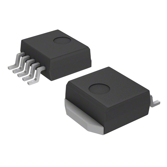
The CS8481 is available in a D2PAK−5.
Features
• 3.3 V/250 mA Primary Output
• 5.0 V/100 mA Secondary Output
• 3.0% Tolerance, Both Outputs
• ON/OFF Control for Primary Output
• Low Quiescent Current Drain (100 �A VOUT2)
• Low Reverse Current
• Protection Features
− Reverse Battery (−15 V)
− 74 V Peak Transient Voltage
− Short Circuit
− Overtemperature
− Overvoltage (34 V)
http://onsemi.com
D2PAK−5
DP SUFFIX
CASE 936AC
1
5
PIN CONNECTIONS AND
MARKING DIAGRAM
Tab = GND
Pin 1. VIN
2. VOUT1
3. GND
4. VOUT2
5. ENABLE
CS8481
AWLYWW
1
A
WL, L
YY, Y
WW, W
= Assembly Location
= Wafer Lot
= Year
= Work Week
ORDERING INFORMATION*
Package
Shipping†
CS8481YDP5
D2PAK−5
50 Units/Rail
CS8481YDPR5
D2PAK−5
750 Tape & Reel
Device
*Consult your local sales representative for SO−8,
SO−16, DIP−8, DIP−16, TO−220−5, and D2PAK−7
packaging options.
†For information on tape and reel specifications,
including part orientation and tape sizes, please
refer to our Tape and Reel Packaging Specifications
Brochure, BRD8011/D.
Semiconductor Components Industries, LLC, 2004
January, 2004 − Rev. 9
1
Publication Order Number:
CS8481/D
�CS8481
Primary Output
VOUT1 (3.3 V)
VIN
ENABLE
+
−
VOUT1SENSE
Current Limit
+
−
Bandgap
Reference
Overvoltage
Shutdown
Thermal
Shutdown
Secondary Output
VOUT2 (5.0 V)
VOUT2SENSE
Current Limit
+
−
Pwr GND
GND
Figure 1. Block Diagram
MAXIMUM RATINGS*
Rating
Value
Unit
30
−15
74
V
V
V
10
V
Internally Limited
−
Maximum Junction Temperature
−40 to +150
°C
Storage Temperature Range
−55 to +150
°C
4.0
kV
230 peak
°C
Input Voltage (VIN)
Operating Range
Reverse Battery
Peak Transient Voltage (60 V Load Dump @ 14 V VIN)
ENABLE
Power Dissipation
Electrostatic Discharge (Human Body Model)
Lead Temperature Soldering
1. 60 second maximum above 183°C
*The maximum package power dissipation must be observed.
Reflow (SMD styles only) (Note 1)
http://onsemi.com
2
�CS8481
ELECTRICAL CHARACTERISTICS: (6.0 V ≤ VIN ≤ 26 V, IOUT1 = IOUT2 = 100 �A, −40°C ≤ TA ≤ 125°C,
−40°C ≤ TC ≤ 125°C; unless otherwise specified.)
Test Conditions
Characteristic
Min
Typ
Max
Unit
3.2
3.3
3.4
V
Primary Output Stage (VOUT1)
Output Voltage, VOUT1
100 �A ≤ IOUT1 ≤ 250 mA
Line Regulation
6.0 V ≤ VIN ≤ 26 V
−
5.0
50
mV
Load Regulation
1.0 mA ≤ IOUT1 ≤ 250 mA, VIN = 14 V
−
5.0
50
mV
Quiescent Current
ENABLE = HIGH, VIN = 16V, IOUT1 = 250 mA
−
22
50
mA
Ripple Rejection
f = 120 Hz, IOUT1 = 125 mA, 7.0 V ≤ VIN ≤ 17 V
60
70
−
dB
Current Limit
9.0 V ≤ VIN ≤ 26 V
260
400
−
mA
Short Circuit Current Limit
VOUT1 = 0 V, VIN = 16 V
25
−
−
mA
Reverse Current
VOUT1 = 3.3 V, VIN = 0 V
−
100
1500
�A
Output Voltage, (VOUT2)
100 �A ≤ IOUT2 ≤ 100 mA
4.85
5.00
5.15
V
Dropout Voltage
IOUT2 = 100 mA
IOUT2 = 100 �A
−
400
100
600
150
mV
mV
Line Regulation
6.0 V ≤ VIN ≤ 26 V
−
5.0
50
mV
Load Regulation
100 �A ≤ IOUT2 ≤ 100 mA, VIN = 14 V
−
5.0
50
mV
Quiescent Current
ENABLE = LOW, VIN = 12.8 V
ENABLE = HIGH, VIN = 16 V, IOUT2 = 100 mA
−
−
100
8.0
150
30
�A
mA
Ripple Rejection
f = 120 Hz; IOUT2 = 10 mA, 7.0 V ≤ VIN ≤ 17 V
60
70
−
dB
Current Limit
9.0 V ≤ VIN ≤ 26 V
105
200
−
mA
Short Circuit Current Limit
VOUT2 = 0 V, VIN = 16 V, IOUT1 = 0 A
25
−
−
mA
Reverse Current
VOUT2 = 5.0 V, VIN = 0 V
−
100
250
�A
Secondary Output (VOUT2)
ENABLE Function (ENABLE)
Input Threshold
ENABLE = LOW, 6.0 V ≤ VIN ≤ 26 V
ENABLE = HIGH, 6.0 V ≤ VIN ≤ 26 V
−
2.0
1.2
1.2
0.8
−
V
V
Input Bias Current
0 V ≤ VENABLE ≤ 5.0 V
−2.0
0
2.0
�A
Note 2
150
180
−
°C
30
34
38
V
Protection Circuits
Overtemperature Threshold
Overvoltage Shutdown
−
2. Guaranteed by Design.
PACKAGE PIN DESCRIPTION
PACKAGE LEAD #
D2PAK−5
LEAD SYMBOL
1
VIN
2
VOUT1
3
GND
4
VOUT2
5
ENABLE
FUNCTION
Supply voltage to IC, usually direct from battery.
3.3 V regulated output which is activated by ENABLE input.
Ground connection.
Standby output 5.0 V, 100 mA capability; always on.
CMOS compatible input lead; switches VOUT1. When ENABLE
is high, VOUT1 is active.
http://onsemi.com
3
�CS8481
DEFINITION OF TERMS
Load Regulation − The change in output voltage for a
change in load current at constant chip temperature.
Long Term Stability − Output voltage stability under
accelerated life−test conditions after 1000 hours with
maximum rated voltage and junction temperature.
Quiescent Current − The part of the positive input
current that does not contribute to the positive load current,
i.e., the regulator ground lead current.
Ripple Rejection − The ratio of the peak−to−peak input
ripple voltage to the peak−to−peak output ripple voltage.
Short Circuit Current Limit − Peak current that can be
delivered by the outPut when forced to 0 V.
Temperature Stability of VOUT − The percentage
change in output voltage for a thermal variation from room
temperature to either temperature extreme.
Current Limit − Peak current that can be delivered to the
output.
Dropout Voltage − The input−output voltage differential
at which the circuit ceases to regulate against further
reduction in input voltage. Measured when the output
voltage has dropped 100 mV from the nominal value
obtained at 14 V input, dropout voltage is dependent upon
load current and junction temperature.
Input Output Differential − The voltage difference
between the unregulated input voltage and the regulated
output voltage for which the regulator will operate.
Input Voltage − The DC voltage applied to the input
terminals with respect to ground.
Line Regulation − The change in output voltage for a
change in the input voltage. The measurement is made under
conditions of low dissipation or by using pulse techniques
such that the average chip temperature is not significantly
affected.
74 V
VIN
14 V
ENABLE
2.0 V
0.8 V
30 V
34 V
3.3 V
14 V
3.0 V
3.3 V
3.3 V
3.3 V
3.3 V
3.3 V
2.4 V
VOUT1
0V
0V
5.0 V
VOUT2 5.0 V
System
Condition
5.0 V
5.0 V
0V
5.0 V
0V
5.0 V
5.0 V
2.4 V
0V
Turn
On
Load
Dump
Low VIN
Line
Noise, Etc.
VOUT1
Short
Circuit
VOUT2
Short
Circuit
Thermal
Shutdown
Turn
Off
Figure 2. Typical Circuit Waveform
APPLICATION NOTES
General
Worst−case is determined at the minimum ambient
temperature and maximum load expected.
Output capacitors can be increased in size to any desired
value above the minimum. One possible purpose of this
would be to maintain the output voltages during brief
conditions of negative input transients that might be
characteristic of a particular system.
Capacitors must also be rated at all ambient temperatures
expected in the system. To maintain regulator stability down
to −40°C, capacitors rated at that temperature must be used.
More information on capacitor selection for SMART
REGULATORs is available in the SMART REGULATOR
application note, “Compensation for Linear Regulators,”
document number SR003AN/D, available through the
Literature Distribution Center or via our website at
http://www.onsemi.com.
The CS8481 is a Micropower dual regulator. All bias
required to operate the internal circuitry is derived from the
standby output, VOUT2. If this output experiences an over
current situation and collapses, then VOUT1 will also
collapse (see Figure 2).
If there is critical circuitry that must remain active under
most conditions it should be connected to VOUT2. Any
circuitry that is likely to be subjected to a short circuit, e.g.,
circuitry outside the module, should be connected to VOUT1.
External Capacitors
Output capacitors are required for stability with the
CS8481. Without them, the regulator outputs will oscillate.
Actual size and type may vary depending upon the
application load and temperature range. Capacitor effective
series resistance (ESR) is also a factor in the IC stability.
http://onsemi.com
4
�CS8481
ENABLE
IIN
The ENABLE function controls VOUT1. When ENABLE
is high, VOUT1 is on. When ENABLE is low, VOUT1 is off.
Calculating Power Dissipation in a
Dual Output Linear Regulator
PD(max) � �VIN(max) � VOUT1(min)�IOUT1(max) �
�VIN(max) � VOUT2(min)�IOUT2(max) � VIN(max)IQ (1)
Heat Sinks
A heat sink effectively increases the surface area of the
package to improve the flow of heat away from the IC and
into the surrounding air.
Each material in the heat flow path between the IC and the
outside environment will have a thermal resistance. Like
series electrical resistances, these resistances are summed to
determine the value of R�JA:
R�JA � R�JC � R�CS � R�SA
The value of R�JA can be compared with those in the
package section of the data sheet. Those packages with
R�JA’s less than the calculated value in equation 2 will keep
the die temperature below 150°C.
In some cases, none of the packages will be sufficient to
dissipate the heat generated by the IC, and an external
heatsink will be required.
R�JC appears in the package section of the data sheet. Like
R�JA, it too is a function of package type. R�CS and R�SA are
functions of the package type, heatsink and the interface
between them. These values appear in heat sink data sheets
of heat sink manufacturers.
VCC
VOUT2
VIN
C2**
C1 *
CS8481
22 �F
ESR < 8 �
�P
VOUT1
22 �F
ESR < 8 �
C3**
Load
(3)
where:
R�JC = the junction−to−case thermal resistance,
R�CS = the case−to−heatsink thermal resistance, and
R�SA = the heatsink−to−ambient thermal resistance.
(2)
VBATT
VOUT2
Figure 3. Dual Output Regulator With Key
Performance Parameters Labeled.
Once the value of PD(max) is known, the maximum
permissible value of R�JA can be calculated:
0.1 �F
IOUT2
IQ
where:
VIN(max) is the maximum input voltage,
VOUT1(min) is the minimum output voltage from VOUT1,
VOUT2(min) is the minimum output voltage from VOUT2,
IOUT1(max) is the maximum output current, for the
application,
IOUT2(max) is the maximum output current, for the
application, and
IQ is the quiescent current the regulator consumes at both
IOUT1(max) and IOUT2(max).
150°C � TA
PD
VOUT1
Control
Features
The maximum power dissipation for a dual output
regulator (Figure 3) is
R�JA �
IOUT1
SMART
REGULATOR
VIN
ENABLE
I/O
GND
GND
* C1 required if regulator is located far from power supply filter.
** C2 and C3 required for stability. Capacitor must operate at minimum temperature expected during system operations.
Figure 4. Test and Application Circuit
http://onsemi.com
5
�CS8481
PACKAGE DIMENSIONS
D2PAK−5
DP SUFFIX
CASE 936AC−01
ISSUE O
For D2PAK Outline and
Dimensions − Contact Factory
PACKAGE THERMAL DATA
Parameter
D2PAK−5
Unit
R�JC
Typical
2.4
°C/W
R�JA
Typical
10−50*
°C/W
* Depending on thermal properties of substrate. R�JA = R�JC + R�CA
SMART REGULATOR is a registered trademark of Semiconductor Components Industries, LLC (SCILLC).
ON Semiconductor and
are registered trademarks of Semiconductor Components Industries, LLC (SCILLC). SCILLC reserves the right to make changes without further notice
to any products herein. SCILLC makes no warranty, representation or guarantee regarding the suitability of its products for any particular purpose, nor does SCILLC assume any liability
arising out of the application or use of any product or circuit, and specifically disclaims any and all liability, including without limitation special, consequential or incidental damages.
“Typical” parameters which may be provided in SCILLC data sheets and/or specifications can and do vary in different applications and actual performance may vary over time. All
operating parameters, including “Typicals” must be validated for each customer application by customer’s technical experts. SCILLC does not convey any license under its patent rights
nor the rights of others. SCILLC products are not designed, intended, or authorized for use as components in systems intended for surgical implant into the body, or other applications
intended to support or sustain life, or for any other application in which the failure of the SCILLC product could create a situation where personal injury or death may occur. Should
Buyer purchase or use SCILLC products for any such unintended or unauthorized application, Buyer shall indemnify and hold SCILLC and its officers, employees, subsidiaries, affiliates,
and distributors harmless against all claims, costs, damages, and expenses, and reasonable attorney fees arising out of, directly or indirectly, any claim of personal injury or death
associated with such unintended or unauthorized use, even if such claim alleges that SCILLC was negligent regarding the design or manufacture of the part. SCILLC is an Equal
Opportunity/Affirmative Action Employer. This literature is subject to all applicable copyright laws and is not for resale in any manner.
PUBLICATION ORDERING INFORMATION
LITERATURE FULFILLMENT:
Literature Distribution Center for ON Semiconductor
P.O. Box 5163, Denver, Colorado 80217 USA
Phone: 303−675−2175 or 800−344−3860 Toll Free USA/Canada
Fax: 303−675−2176 or 800−344−3867 Toll Free USA/Canada
Email: orderlit@onsemi.com
N. American Technical Support: 800−282−9855 Toll Free
USA/Canada
ON Semiconductor Website: http://onsemi.com
Order Literature: http://www.onsemi.com/litorder
Japan: ON Semiconductor, Japan Customer Focus Center
2−9−1 Kamimeguro, Meguro−ku, Tokyo, Japan 153−0051
Phone: 81−3−5773−3850
http://onsemi.com
6
For additional information, please contact your
local Sales Representative.
CS8481/D
�


 工商网监
湘ICP备2023018690号
工商网监
湘ICP备2023018690号
