Revised July 2001
DM7442A
BCD to Decimal Decoder
General Description
Features
These BCD-to-decimal decoders consist of eight inverters
and ten, four-input NAND gates. The inverters are connected in pairs to make BCD input data available for
decoding by the NAND gates. Full decoding of input logic
ensures that all outputs remain off for all invalid (10–15)
input conditions.
■ Diode clamped inputs
■ Also for application as 4-line-to-16-line decoders;
3-line-to-8-line decoders
■ All outputs are high for invalid input conditions
■ Typical power dissipation 140 mW
■ Typical propagation delay 17 ns
Ordering Code:
Order Number
DM7442AN
Package Number
N16E
Package Description
16-Lead Plastic Dual-In-Line Package (PDIP), JEDEC MS-001, 0.300" Wide
Connection Diagram
© 2001 Fairchild Semiconductor Corporation
DS006516
www.fairchildsemi.com
DM7442A BCD to Decimal Decoder
August 1986
�DM7442A
Function Table
No.
BCD Input
Decimal Output
D
C
B
A
0
1
2
3
4
5
6
7
8
9
0
L
L
L
L
L
H
H
H
H
H
H
H
H
H
1
L
L
L
H
H
L
H
H
H
H
H
H
H
H
2
L
L
H
L
H
H
L
H
H
H
H
H
H
H
3
L
L
H
H
H
H
H
L
H
H
H
H
H
H
4
L
H
L
L
H
H
H
H
L
H
H
H
H
H
5
L
H
L
H
H
H
H
H
H
L
H
H
H
H
6
L
H
H
L
H
H
H
H
H
H
L
H
H
H
7
L
H
H
H
H
H
H
H
H
H
H
L
H
H
8
H
L
L
L
H
H
H
H
H
H
H
H
L
H
9
H
L
L
H
H
H
H
H
H
H
H
H
H
L
I
H
L
H
L
H
H
H
H
H
H
H
H
H
H
N
H
L
H
H
H
H
H
H
H
H
H
H
H
H
V
H
H
L
L
H
H
H
H
H
H
H
H
H
H
A
H
H
L
H
H
H
H
H
H
H
H
H
H
H
L
H
H
H
L
H
H
H
H
H
H
H
H
H
H
I
H
H
H
H
H
H
H
H
H
H
H
H
H
H
D
H = HIGH Level
L = LOW Level
Logic Diagram
www.fairchildsemi.com
2
�Supply Voltage
Note 1: The “Absolute Maximum Ratings” are those values beyond which
the safety of the device cannot be guaranteed. The device should not be
operated at these limits. The parametric values defined in the Electrical
Characteristics tables are not guaranteed at the absolute maximum ratings.
The “Recommended Operating Conditions” table will define the conditions
for actual device operation.
7V
Input Voltage
5.5V
0°C to +70°C
Operating Free Air Temperature Range
Storage Temperature Range
−65°C to +150°C
Recommended Operating Conditions
Symbol
Parameter
Min
Nom
Max
Units
4.75
5
5.25
V
VCC
Supply Voltage
VIH
HIGH Level Input Voltage
VIL
LOW Level Input Voltage
0.8
V
IOH
HIGH Level Output Current
−0.8
mA
IOL
LOW Level Output Current
16
mA
TA
Free Air Operating Temperature
70
°C
2
V
0
Electrical Characteristics
over recommended operating free air temperature range (unless otherwise noted)
Symbol
Parameter
Conditions
VI
Input Clamp Voltage
VCC = Min, II = −12 mA
VOH
HIGH Level
VCC = Min, IOH = Max
Output Voltage
VIL = Max, VIH = Min
LOW Level
VCC = Min, IOL = Max
Output Voltage
VIH = Min, VIL = Max
VOL
Min
2.4
Typ
(Note 2)
Max
Units
−1.5
V
3.4
0.2
V
0.4
V
mA
II
Input Current @ Max Input Voltage
VCC = Max, VI = 5.5V
1
IIH
HIGH Level Input Current
VCC = Max, VI = 2.4V
40
µA
IIL
LOW Level Input Current
VCC = Max, VI = 0.4V
−1.6
mA
IOS
Short Circuit Output Current
VCC = Max (Note 3)
ICC
Supply Current
VCC = Max (Note 4)
−18
−55
mA
28
56
mA
Min
Max
Units
25
ns
30
ns
25
ns
30
ns
Note 2: All typicals are at VCC = 5V, TA = 25°C.
Note 3: Not more than one output should be shorted at a time.
Note 4: ICC is measured with all outputs open and all inputs grounded.
Switching Characteristics
at VCC = 5V and TA = 25°C
Symbol
tPHL
Parameter
Conditions
Propagation Delay Time
CL = 15 pF
HIGH-to-LOW Level Output
RL = 400Ω
from A, B, C or D through
2 Levels of Logic
tPHL
Propagation Delay Time
HIGH-to-LOW Level Output
from A, B, C or D through
3 Levels of Logic
tPLH
Propagation Delay Time
LOW-to-HIGH Level Output
from A, B, C or D through
2 Levels of Logic
tPLH
Propagation Delay Time
LOW-to-HIGH Level Output
from A, B, C or D through
3 Levels of Logic
3
www.fairchildsemi.com
DM7442A
Absolute Maximum Ratings(Note 1)
�DM7442A BCD to Decimal Decoder
Physical Dimensions inches (millimeters) unless otherwise noted
16-Lead Plastic Dual-In-Line Package (PDIP), JEDEC MS-001, 0.300" Wide
Package Number N16E
Fairchild does not assume any responsibility for use of any circuitry described, no circuit patent licenses are implied and
Fairchild reserves the right at any time without notice to change said circuitry and specifications.
LIFE SUPPORT POLICY
FAIRCHILD’S PRODUCTS ARE NOT AUTHORIZED FOR USE AS CRITICAL COMPONENTS IN LIFE SUPPORT
DEVICES OR SYSTEMS WITHOUT THE EXPRESS WRITTEN APPROVAL OF THE PRESIDENT OF FAIRCHILD
SEMICONDUCTOR CORPORATION. As used herein:
2. A critical component in any component of a life support
device or system whose failure to perform can be reasonably expected to cause the failure of the life support
device or system, or to affect its safety or effectiveness.
1. Life support devices or systems are devices or systems
which, (a) are intended for surgical implant into the
body, or (b) support or sustain life, and (c) whose failure
to perform when properly used in accordance with
instructions for use provided in the labeling, can be reasonably expected to result in a significant injury to the
user.
www.fairchildsemi.com
www.fairchildsemi.com
4
�
很抱歉,暂时无法提供与“DM7442AN”相匹配的价格&库存,您可以联系我们找货
免费人工找货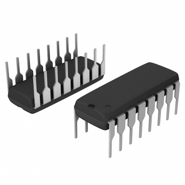


 工商网监
湘ICP备2023018690号
工商网监
湘ICP备2023018690号
