ES1A - ES1D
ES1A - ES1D
Features
•
For surface mount applications.
•
Glass passivated junction.
•
Low profile package.
•
Easy pick and place.
•
Built-in strain relief.
•
Superfast recovery times for
high efficiency.
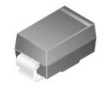
SMA/DO-214AC
COLOR BAND DENOTES CATHODE
Fast Rectifiers
Absolute Maximum Ratings*
Symbol
TA = 25°C unless otherwise noted
Value
Parameter
1A
50
1B
100
1C
150
1.0
1D
200
Units
VRRM
IF(AV)
Maximum Repetitive Reverse Voltage
Average Rectified Forward Current, @ TA=120°C
IFSM
Non-repetitive Peak Forward Surge Current
8.3 ms Single Half-Sine-Wave
Storage Temperature Range
30
A
-50 to +150
°C
Operating Junction Temperature
-50 to +150
°C
Tstg
TJ
V
A
*These ratings are limiting values above which the serviceability of any semiconductor device may be impaired.
Thermal Characteristics
Parameter
Symbol
Value
Units
PD
Power Dissipation
1.47
W
RθJA
Thermal Resistance, Junction to Ambient*
85
°C/W
RθJL
Thermal Resistance, Junction to Lead*
35
°C/W
*Device mounted on FR-4 PCB 0.013 mm.
Electrical Characteristics
Symbol
TA = 25°C unless otherwise noted
Device
Parameter
1A
VF
Forward Voltage @ 1.0 A
trr
Reverse Recovery Time
IF = 0.5 A, IR = 1.0 A, IRR = 0.25 A
Reverse Current @ rated VR
IR
CT
Total Capacitance
VR = 4.0 V, f = 1.0 MHz
2010 Semiconductor Components Industries, LLC.
October-2017, Rev. 3
TA = 25°C
TA = 100°C
1B
1C
Units
1D
0.92
V
15
ns
5.0
100
µA
µA
pF
7.0
Publication Order Number:
ES1A/D
�ES1A - ES1D
10
1.5
1.25
Forward Current, IF [A]
Average Rectified Forward Current, IF [A]
Typical Characteristics
1
0.75
RESISTIVE OR
INDUCTIVE LOAD
P.C.B. MOUNTED
ON 0.2 x 0.2"
(5.0 x 5.0 mm)
COPPER PAD AREAS
0.5
0.25
0
0
25
50
75
100
125
Ambient Temperature [ºC]
150
0.1
0.01
TA = 25º C
Pulse Width = 300µ
µs
2% Duty Cycle
0.001
0.4
175
Figure 1. Forward Current Derating Curve
0.6
0.8
1
1.2
Forward Voltage, VF [V]
1.4
Figure 2. Forward Voltage Characteristics
1000
30
25
Reverse Current, IR [uA]
Peak Forward Surge Current, IFSM [A]
1
20
15
10
5
0
1
2
5
10
20
Number of Cycles at 60Hz
50
100
Figure 3. Non-Repetitive Surge Current
100
T A = 125 º C
10
TA = 75º C
1
T A = 25º C
0.1
0
60
80
100
120
140
20
40
Percent of Rated Peak Reverse Voltage [%]
Figure 4. Reverse Current vs Reverse Voltage
Total Capacitance, C T [pF]
14
12
10
8
6
4
2
0
0.1
1
10
Reverse Voltage, V R [V]
100
Figure 5. Total Capacitance
50Ω
NONINDUCTIVE
50Ω
NONINDUCTIVE
+0.5A
trr
(-)
DUT
50V
(approx)
50Ω
NONINDUCTIVE
Pulse
Generator
(Note 2)
0
-0.25A
(+)
OSCILLOSCOPE
(Note 1)
NOTES:
1. Rise time = 7.0 ns max; Input impedance = 1.0 megaohm 22 pf.
2. Rise time = 10 ns max; Source impedance = 50 ohms.
-1.0A
1.0cm
SET TIME BASE FOR
5/ 10 ns/ cm
Reverse Recovery Time Characterstic and Test Circuit Diagram
www.onsemi.com
2
�ON Semiconductor and
are trademarks of Semiconductor Components Industries, LLC dba ON Semiconductor or its subsidiaries in the United States and/or other countries.
ON Semiconductor owns the rights to a number of patents, trademarks, copyrights, trade secrets, and other intellectual property. A listing of ON Semiconductor’s product/patent
coverage may be accessed at www.onsemi.com/site/pdf/Patent−Marking.pdf. ON Semiconductor reserves the right to make changes without further notice to any products herein.
ON Semiconductor makes no warranty, representation or guarantee regarding the suitability of its products for any particular purpose, nor does ON Semiconductor assume any liability
arising out of the application or use of any product or circuit, and specifically disclaims any and all liability, including without limitation special, consequential or incidental damages.
Buyer is responsible for its products and applications using ON Semiconductor products, including compliance with all laws, regulations and safety requirements or standards,
regardless of any support or applications information provided by ON Semiconductor. “Typical” parameters which may be provided in ON Semiconductor data sheets and/or
specifications can and do vary in different applications and actual performance may vary over time. All operating parameters, including “Typicals” must be validated for each customer
application by customer’s technical experts. ON Semiconductor does not convey any license under its patent rights nor the rights of others. ON Semiconductor products are not
designed, intended, or authorized for use as a critical component in life support systems or any FDA Class 3 medical devices or medical devices with a same or similar classification
in a foreign jurisdiction or any devices intended for implantation in the human body. Should Buyer purchase or use ON Semiconductor products for any such unintended or unauthorized
application, Buyer shall indemnify and hold ON Semiconductor and its officers, employees, subsidiaries, affiliates, and distributors harmless against all claims, costs, damages, and
expenses, and reasonable attorney fees arising out of, directly or indirectly, any claim of personal injury or death associated with such unintended or unauthorized use, even if such
claim alleges that ON Semiconductor was negligent regarding the design or manufacture of the part. ON Semiconductor is an Equal Opportunity/Affirmative Action Employer. This
literature is subject to all applicable copyright laws and is not for resale in any manner.
PUBLICATION ORDERING INFORMATION
LITERATURE FULFILLMENT:
Literature Distribution Center for ON Semiconductor
19521 E. 32nd Pkwy, Aurora, Colorado 80011 USA
Phone: 303−675−2175 or 800−344−3860 Toll Free USA/Canada
Fax: 303−675−2176 or 800−344−3867 Toll Free USA/Canada
Email: orderlit@onsemi.com
❖
© Semiconductor Components Industries, LLC
N. American Technical Support: 800−282−9855 Toll Free
USA/Canada
Europe, Middle East and Africa Technical Support:
Phone: 421 33 790 2910
Japan Customer Focus Center
Phone: 81−3−5817−1050
ON Semiconductor Website: www.onsemi.com
Order Literature: http://www.onsemi.com/orderlit
For additional information, please contact your local
Sales Representative
www.onsemi.com
�


 工商网监
湘ICP备2023018690号
工商网监
湘ICP备2023018690号


