ON Semiconductor
Is Now
To learn more about onsemi™, please visit our website at
www.onsemi.com
onsemi and and other names, marks, and brands are registered and/or common law trademarks of Semiconductor Components Industries, LLC dba “onsemi” or its affiliates and/or
subsidiaries in the United States and/or other countries. onsemi owns the rights to a number of patents, trademarks, copyrights, trade secrets, and other intellectual property. A listing of onsemi
product/patent coverage may be accessed at www.onsemi.com/site/pdf/Patent-Marking.pdf. onsemi reserves the right to make changes at any time to any products or information herein, without
notice. The information herein is provided “as-is” and onsemi makes no warranty, representation or guarantee regarding the accuracy of the information, product features, availability, functionality,
or suitability of its products for any particular purpose, nor does onsemi assume any liability arising out of the application or use of any product or circuit, and specifically disclaims any and all
liability, including without limitation special, consequential or incidental damages. Buyer is responsible for its products and applications using onsemi products, including compliance with all laws,
regulations and safety requirements or standards, regardless of any support or applications information provided by onsemi. “Typical” parameters which may be provided in onsemi data sheets and/
or specifications can and do vary in different applications and actual performance may vary over time. All operating parameters, including “Typicals” must be validated for each customer application
by customer’s technical experts. onsemi does not convey any license under any of its intellectual property rights nor the rights of others. onsemi products are not designed, intended, or authorized
for use as a critical component in life support systems or any FDA Class 3 medical devices or medical devices with a same or similar classification in a foreign jurisdiction or any devices intended for
implantation in the human body. Should Buyer purchase or use onsemi products for any such unintended or unauthorized application, Buyer shall indemnify and hold onsemi and its officers, employees,
subsidiaries, affiliates, and distributors harmless against all claims, costs, damages, and expenses, and reasonable attorney fees arising out of, directly or indirectly, any claim of personal injury or death
associated with such unintended or unauthorized use, even if such claim alleges that onsemi was negligent regarding the design or manufacture of the part. onsemi is an Equal Opportunity/Affirmative
Action Employer. This literature is subject to all applicable copyright laws and is not for resale in any manner. Other names and brands may be claimed as the property of others.
�Features
Description
6 MHz Fixed-Frequency Operation
35 µA Typical Quiescent Current
The FAN5361 is a 600 mA or 750 mA, step-dow n, sw itching
voltage regulator that delivers a fixed output from a 2.3 V to
5.5 V input voltage supply. Using a proprietary architecture
w ith synchronous rectification, the FAN5361 is capable of
delivering a peak efficiency of 92%, w hile maintaining
efficiency over 80% at load currents as low as 1 mA.
Best-in-Class Load Transient Response
Best-in-Class Efficiency
600 mA or 750 mA Output Current Capability
2.3 V to 5.5 V Input Voltage Range
The regulator operates at a nominal fixed frequency of
6 MHz, w hich reduces the value of the external components
to 470 nH for the output inductor and 4.7 µF for the output
capacitor. The PWM modulator can be synchronized to an
external frequency source.
1.0 to 1.90 V Fixed Output Voltage
Low Ripple Light-Load PFM Mode
Forced PWM and External Clock Synchronization
Internal Soft-Start
Input Under-Voltage Lockout (UVLO)
Thermal Shutdow n and Overload Protection
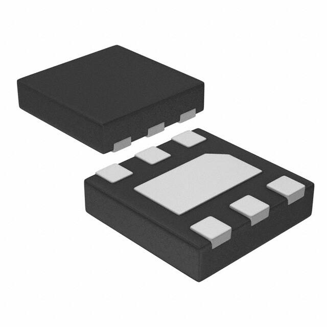
6-bump WLCSP, 0.4 mm Pitch
6-pin 2 x 2 mm UMLP
Applications
Cell Phones, Smart Phones
®
Tablets, Netbooks , Ultra-Mobile PCs
®
®
3G, LTE, WiMAX™, WiBro , and WiFi Data Cards
Gaming Devices, Digital CamerasDC/DC Micro Modules
At moderate and light loads, pulse frequency modulation is
used to operate the device in pow er-save mode w ith a
typical quiescent current of 35 µA. Even w ith such a low
quiescent current, the part exhibits excellent transient
response during large load sw ings. At higher loads, the
system automatically sw itches to fixed-frequency control,
operating at 6 MHz. In shutdow n mode, the supply current
drops below 1 µA, reducing pow er consumption. For
applications that require minimum ripple or fixed frequency,
PFM mode can be disabled using the MODE pin.
The FAN5361 is available in 6-bump, 0.4 mm pitch, WaferLevel Chip-Scale Package (WLCSP) and a 6-lead 2 x 2 mm
ultra-thin MLP package (UMLP).
Typical Applications
MODE
L1
SW
470nH
FB
4.7F
A1
A2
B1
B2
C1
C2
FB
VIN
EN
COUT
CIN
2.2F
4.7F
GND
L1
SW
2
6
(AGND)
5
GND
EN
470nH
MODE
COUT
Figure 1.
1
3
4
CIN
2.2F
VIN
Typical Applications
All trademarks are the property of their respective owners.
© 2008 Semiconductor Components Industries, LLC.
October-2017, Rev. 2
Publication Order Number:
FAN5361/D
FAN5361 — 6 MHz, 600 mA / 750 mA Synchronous Buck Regulator
FAN5361
6 MHz, 600 mA / 750 mA Synchronous Buck Regulator
�Output
Voltage (1)
Part Number
FAN5361UC123X*
1.233 V
FAN5361UC182X
1.820 V
FAN5361UC19X
1.900 V
FAN5361UMP123X
1.233 V
FAN5361UMP15X
1.500 V
FAN5361UMP182X
1.820 V
Package
Temperature Range
Packing
–40 to +85°C
Tape and Reel
WLCSP-6, 0.4 mm Pitch
6-Lead, 2 x 2 mm UMLP
Note:
1. Other voltage options available on request. Contact a ON Semiconductor representative.
*
This device is End of Life. Please contact sales for additional information and assistance with replacement devices.
Pin Configurations
MODE
A1
A2
VIN
VIN
A2
A1
MODE
SW
B1
B2
EN
EN
B2
B1
SW
FB
C1
C2
GND
GND
C2
C1
FB
Figure 2.
WLCSP, Bum ps Facing Dow n
Figure 3.
FB 1
SW 2
6 GND
P1
(GND)
5
MODE 3
Figure 4.
WLCSP, Bum ps Facing Up
EN
4 VIN
UMLP, Leads Facing Dow n
Pin Definitions
Pin #
WLCSP UMLP
Name
Description
MODE. Logic 1 on this pin forces the IC to stay in PWM mode. A logic 0 allow s the IC to
automatically sw itch to PFM during light loads. The regulator also synchronizes its sw itching
MODE
frequency to four times the frequency provided on this pin. Do not leave this pin floating. When
tying HIGH, use at least 1kΩ series resistor if V IN is expected to exceed 4.5 V.
A1
3
B1
2
SW
Sw itching Node . Connect to output inductor.
C1
1
FB
Feedback / V OUT. Connect to output voltage.
C2
6
GND
B2
5
EN
Enable. The device is in shutdow n mode w hen voltage to this pin is 1.2 V. Do not leave this pin floating. When tying HIGH, use at least 1 kΩ series resistor if V IN is
expected to exceed 4.5 V.
A2
4
VIN
Input Voltage . Connect to input pow er source.
Ground. Pow er and IC ground. All signals are referenced to this pin.
www.onsemi.com
2
FAN5361 — 6 MHz, 600 mA / 750 mA Synchronous Buck Regulator
Ordering Information
�Stresses exceeding the absolute maximum ratings may damage the device. The device may not function or be operable above
the recommended operating conditions and stressing the parts to these levels is not recommended. In addition, extended
exposure to stresses above the recommended operating conditions may affect device reliability. The absolute maximum ratings
are stress ratings only.
Symbol
V IN
V SW
V CTRL
Parameter
Input Voltage
Max.
–0.3
7.0
Unit
V
(2)
V
(2)
V
(2)
V
Voltage on SW Pin
–0.3
V IN + 0.3
EN and MODE Pin Voltage
–0.3
V IN + 0.3
–0.3
Other Pins
ESD
Min.
Electrostatic Discharge
Protection Level
V IN + 0.3
Human Body Model per JESD22-A114
4.0
Charged Device Model per JESD22-C101
1.5
kV
TJ
Junction Temperature
–40
+150
°C
TSTG
Storage Temperature
–65
+150
°C
+260
°C
TL
Lead Soldering Temperature, 10 Seconds
Note:
2. Lesser of 7 V or V IN+0.3 V.
Recommended Operating Conditions
The Recommended Operating Conditions table defines the conditions for actual device operation. Recommended operating
conditions are specified to ensure optimal performance to the datasheet specifications. ON Semiconductor does not recommend
exceeding them or designing to Absolute Maximum Ratings.
Symbol
Parameter
V CC
Supply Voltage Range
IOUT
Output Current
L
CIN
COUT
Min.
Typ.
2.3
0
Max.
Unit
5.5
V
600
mA
Inductor
0.47
µH
Input Capacitor
2.2
µF
12.0
µF
–40
+85
°C
–40
+125
°C
Output Capacitor
1.6
TA
Operating Ambient Temperature
TJ
Operating Junction Temperature
4.7
Thermal Properties
Junction-to-ambient thermal resistance is a function of application and board layout. This data is measured w ith four -layer 1s2p
boards in accordance to JEDEC standard JESD51. Special attention must be paid not to exceed junction temperature T J(max) at a
given ambient temperate TA.
Symbol
JA
Parameter
Junction-to-Ambient Thermal Resistance
www.onsemi.com
3
Typical
Unit
WLCSP
150
°C/W
UMLP
49
°C/W
FAN5361 — 6 MHz, 600 mA / 750 mA Synchronous Buck Regulator
Absolute Maximum Ratings
�Minimum and maximum values are at V IN = V EN = 2.3V to 5.5V, V MODE = 0V (AUTO Mode), TA = -40°C to +85°C; circuit of
Figure 1, unless otherw ise noted. Typical values are at TA = 25°C, V IN = V EN = 3.6 V.
Symbol
Parameter
Conditions
Min.
Typ.
Max.
Unit
35
55
µA
Pow er Supplies
IQ
I(SD)
No Load, Not Sw itching
Quiescent Current
PWM Mode
6
mA
Shutdow n Supply Current
V IN = 3.6 V, EN = GND
0.05
1.00
µA
V UVLO
Under-Voltage Lockout Threshold
Rising V IN
2.15
2.25
V
V UVHYST
Under-Voltage Lockout Hysteresis
150
mV
Logic Inputs: EN and MODE Pins
V IH
Enable HIGH-Level Input Voltage
V IL
Enable LOW-Level Input Voltage
V LHYST
Logic Input Hysteresis Voltage
IIN
Enable Input Leakage Current
1.2
V
0.4
100
Pin to V IN or GND
V
mV
0.01
1.00
µA
Sw itching and Synchronization
f SW
(3)
V IN = 3.6 V, TA = 25°C
5.4
6.0
6.6
MHz
Square Wave at MODE Input
1.3
1.5
1.7
MHz
1.832
1.900
1.957
PWM Mode
1.832
1.900
1.938
ILOAD = 0 to 600 mA
1.784
1.820
1.875
PWM Mode
1.784
1.820
1.856
ILOAD = 0 to 600 mA
1.470
1.500
1.545
PWM Mode
1.470
1.500
1.530
ILOAD = 0 to 600 mA
1.207
1.233
1.272
PWM Mode
1.207
1.233
1.259
From EN Rising Edge
180
300
PMOS On Resistance
V IN = V GS = 3.6 V
350
NMOS On Resistance
V IN = V GS = 3.6 V
225
PMOS Open-Loop Peak Current
(5)
Limit
V OUT = 1.233 V, 1.5 V, 1.82 V
900
1100
1250
V OUT = 1.9 V
1180
1375
1550
TTSD
Thermal Shutdow n
CCM Only
THYS
Thermal Shutdow n Hysteresis
f SYNC
Sw itching Frequency
MODE Synchronization Range
(3)
Regulation
1.900 V
1.820 V
VO
Output Voltage
Accuracy
1.500 V
1.233 V
tSS
Soft-Start
ILOAD = 0 to 750 mA
(4)
(4)
V
µs
Output Driver
RDS(on)
ILIM(OL)
m
150
°C
15
°C
Notes:
3. Limited by the effect of tOFF minimum (see Figure 14 and Figure 15 in Typical Performance Characteristics).
4. Output voltage accuracy minimum: 1.862 V for V IN 2.7 to 5.5 V on 1.9 V option.
5. Refer to Operation Description and Typical Characteristics for closed-loop data.
www.onsemi.com
4
mA
FAN5361 — 6 MHz, 600 mA / 750 mA Synchronous Buck Regulator
Electrical Characteristics
�Unless otherw ise noted, V IN = V EN = 3.6 V, V MODE = 0 V (AUTO Mode), V OUT = 1.82 V, TA = 25°C.
100%
100%
95%
95%
90%
90%
85%
80%
Efficiency
Efficiency
85%
Auto 2.3VIN
75%
70%
Auto 2.7VIN
65%
Auto 3.6VIN
80%
75%
25C
70%
85C
65%
60%
60%
Auto 4.2VIN
55%
-30C
55%
50%
50%
1
10
100
1000
1
10
I LOAD Output Current (mA)
Figure 5.
Efficiency vs. Load Current and Input Supply Figure 6.
1000
Efficiency vs. Load Current and Tem perature
100%
100%
95%
95%
90%
90%
85%
85%
Efficiency
Efficiency
100
I LOAD Output Current (mA)
80%
75%
VIN=2.3V
70%
80%
75%
70%
VIN=2.7V
65%
65%
VIN=3.6V
60%
55%
55%
50%
50%
1
10
100
Auto PFM/PWM
60%
VIN=4.2V
1000
Forced PWM
1
10
I LOAD Output Current (mA)
Figure 7.
100
1000
I LOAD Output Current (mA)
1.233 V OUT Efficiency vs. Load Current
and Supply
Figure 8.
Efficiency, Auto PWM/PFM vs. Forced PWM
1.248
1.84
VIN=2.3V
1.243
VIN=2.7V
1.83
VOUT (V)
VOUT (V)
VIN=3.6V
1.82
VIN=2.3V
1.238
VIN=4.2V
1.233
VIN=2.7V
1.81
1.228
VIN=3.6V
VIN=4.2V
1.223
1.80
0
100
200
300
400
500
0.0
600
Figure 9.
Load Regulation
0.1
0.2
0.3
0.4
0.5
0.6
I LOAD Output Current (A)
Load Current (mA)
Figure 10. 1.233 V OUT Load Regulation vs. Input Supply
www.onsemi.com
5
FAN5361 — 6 MHz, 600 mA / 750 mA Synchronous Buck Regulator
Typical Performance Characteristics
�Unless otherw ise noted, V IN = V EN = 3.6 V, V MODE = 0 V (AUTO Mode), V OUT = 1.82 V, TA = 25°C.
1.830
45
40
3.6VIN
1.825
5.5VIN
2.5VIN
30
1.820
Vout (mVpp)
VOUT (V)
35
1.815
25
20
15
10
1.810
Auto PWM/PFM
Forced PWM
5
1.805
0
1
10
100
1,000
0
100
200
I LOAD Output Current (mA)
Figure 11. Load Regulation, Auto PFM / PWM and
Forced PWM
400
500
600
Figure 12. 1.82 V OUT Peak-to-Peak Output Voltage
Ripple
7
30
Switching Frequency (MHz)
FPWM Mode
3.6VIN
25
5.5VIN
2.5VIN
20
Vout (mVpp)
300
Load Current (mA)
15
10
5
6
5
4
3
VIN>2.9V
VIN=2.7V
2
VIN=2.5V
VIN=2.3V
0
1
0
100
200
300
400
500
600
0
0.1
0.2
0.3
Load Current (mA)
Figure 13. 1.233 V OUT Peak-to-Peak Output Voltage
Ripple
0.5
0.6
Figure 14. Effect of t OFF(MIN) on Reducing Sw itching
Frequency
7
350
FPWM Mode
6
300
5
Load Current (mA)
Switching Frequency (MHz)
0.4
Load Current (A)
4
3
VIN>2.4V
2
Always PWM
250
200
The switching mode changes
at these borders
150
100
Always PFM
50
1
PFM border
VIN=2.3V
PWM border
0
0
0
0.1
0.2
0.3
0.4
0.5
0.6
2.5
3.0
3.5
4.0
4.5
5.0
Input Voltage (V)
Load Current (A)
Figure 15. 1.233 V OUT Effect of t OFF(MIN) on Reducing
Sw itching Frequency
www.onsemi.com
6
Figure 16. PFM / PWM Boundaries
5.5
FAN5361 — 6 MHz, 600 mA / 750 mA Synchronous Buck Regulator
Typical Performance Characteristics (Continued)
�Unless otherw ise noted, V IN = V EN = 3.6 V, V MODE = 0 V (AUTO Mode), V OUT = 1.82 V, TA = 25°C.
42
250
Always PWM
40
Quiescent Current (A)
The switching mode changes
at these borders
150
100
Always PFM
50
PFM border
38
36
34
32
PWM border
VEN=VIN
0
VEN=1.8V
2.5
3.0
3.5
4.0
4.5
5.0
30
5.5
2.0
2.5
3.0
3.5
Input Voltage(V)
0.18
VIN=5.5V
VEN=0V
0.14
0.12
0.10
0.08
0.06
0.04
0.02
0.00
-40
4.5
5.0
Figure 18. Quiescent Current vs. Input Voltage
0.20
0.16
4.0
VIN Input Voltage (V)
Figure 17. 1.233 V OUT PFM / PWM Boundaries
Supply Current (µA)
Load Current (mA)
200
-20
0
20
40
60
80
Ambient Temperature (°C)
Figure 19. Shutdow n Current vs. Tem perature
www.onsemi.com
7
5.5
FAN5361 — 6 MHz, 600 mA / 750 mA Synchronous Buck Regulator
Typical Performance Characteristics (Continued)
�Unless otherw ise noted, V IN = V EN = 3.6 V, V MODE = 0 V (AUTO Mode), V OUT = 1.82 V, TA = 25°C, 5µs/div. horizontal sw eep.
Figure 20. Line Transient 3.3 V IN to 3.9 V IN,
50 m A Load, 10 µs/div.
Figure 21. Line Transient 3.3 V IN to 3.9 V IN,
250 m A Load, 10 µs/div.
Figure 22.
Com bined Line/Load Transient 3.9 to
Figure 23. Com bined Line/Load Transie nt 3.3 to 3.9 V IN
3.3 V IN Com bined w ith 40 m A to 400 m A Load Transient
Com bined w ith 400 m A to 40 m A Load Transient
Figure 24. Load Transient 0 to 150 m A, 2.5 V IN
Figure 25. Load Transient 50 to 250 m A, 2.5 V IN
www.onsemi.com
8
FAN5361 — 6 MHz, 600 mA / 750 mA Synchronous Buck Regulator
Typical Performance Characteristics (Continued)
�Unless otherw ise noted, V IN = V EN = 3.6 V, V MODE = 0 V (AUTO Mode), V OUT = 1.82 V, TA = 25°C, 5 µs/div. horizontal sw eep.
Figure 26. Load Transient 150 to 400 m A, 2.5 V IN
Figure 27. Load Transient 0 to 150 m A, 3.6 V IN
Figure 28. Load Transient 50 to 250 m A, 3.6 V IN
Figure 29. Load Transient 150 to 400 m A, 3.6 V IN
Figure 30. Load Transient 0 to 150 m A, 4.5 V IN
Figure 31. Load Transient 50 to 250 m A, 4.5 V IN
Figure 32. Load Transient 150 to 400 m A, 4.5 V IN
www.onsemi.com
9
FAN5361 — 6 MHz, 600 mA / 750 mA Synchronous Buck Regulator
Typical Performance Characteristics (Continued)
�Unless otherw ise noted, V IN = V EN = 3.6 V, V MODE = 0 V (AUTO Mode), V OUT = 1.82 V, TA = 25°C, 5 µs/div. horizontal sw eep.
Figure 33. Metallic Short Applied at V OUT, 50 μs/div.
Figure 34. Metallic Short Applied at V OUT
Figure 35. Over-Current Fault Response,
RLOAD = 1 Ω, 50 μs/div.
Figure 36. Over-Current Fault Response, RLOAD = 1 Ω
Figure 37. Overload Recovery to Light Load, 50 μs/div.
Figure 38. Soft-Start, RLOAD = 50 Ω, 20 μs/div.
www.onsemi.com
10
FAN5361 — 6 MHz, 600 mA / 750 mA Synchronous Buck Regulator
Typical Performance Characteristics (Continued)
�Unless otherw ise noted, V IN = V EN = 3.6 V, V MODE = 0 V (AUTO Mode), V OUT = 1.82 V, TA = 25°C.
SW
Figure 39. SW-Node Jitter (Infinite Persistence), ILOAD = 200 m A, 50 ns/div.
Figure 40. Pow er Supply Rejection Ratio at 300 m A Load
www.onsemi.com
11
FAN5361 — 6 MHz, 600 mA / 750 mA Synchronous Buck Regulator
Typical Performance Characteristics (Continued)
�The FAN5361 is a 600 mA or 750 mA, step-dow n, sw itching
voltage regulator that delivers a fixed output from an input
voltage supply of 2.3 V to 5.5 V. Using a proprietary
architecture w ith synchronous rectification, the FAN5361 is
capable of delivering a peak efficiency of 92%, w hile
maintaining efficiency over 80% at load currents as low as
1 mA. The regulator operates at a nominal frequency of
6 MHz at full load, w hich reduces the value of the external
components to 470 nH for the inductor and 4.7 µF for the
output capacitor.
Control Scheme
The FAN5361 uses a proprietary, non-linear, fixed-frequency
PWM modulator to deliver a fast load transient response,
w hile maintaining a constant sw itching frequency over a w ide
range of operating conditions. The regulator performance is
independent of the output capacitor ESR, allow ing for the use
of ceramic output capacitors. Although this type of operation
normally results in a sw itching frequency that varies w ith input
voltage and load current, an internal frequency loop holds the
sw itching frequency constant over a large range of input
voltages and load currents.
For very light loads, the FAN5361 operates in Discontinuous
Current Mode (DCM) single-pulse PFM mode, w hich
produces low output ripple compared w ith other PFM
architectures. Transition betw een PWM and PFM is
seamless, w ith a glitch of less than 18 mV at V OUT during the
transition betw een DCM and CCM modes.
Combined
w ith
exceptional
transient
response
characteristics, the very low quiescent current of the
controller (35 µA) maintains high efficiency; even at very light
loads, w hile preserving fast transient response for
applications requiring tight output regulation.
Enable and Soft-Start
When EN is LOW, all circuits in FAN5361 are off and the IC
draw s ~50 nA of current. When EN is HIGH and V IN is above
its UVLO threshold, the regulator begins a soft-start cycle. The
output ramp during soft-start is a fixed slew rate of 50 mV/s
from 0 to 1 V OUT, then 12.5 mV/s until the output reaches its
setpoint. Regardless of the state of the MODE pin, PFM mode
is enabled to prevent current from being discharged from COUT
if soft-start begins w hen COUT is charged.
The IC may fail to start if heavy load is applied during startup
and/or if excessive COUT is used. This is due to the currentlimit fault response, w hich protects the IC in the event of an
over-current condition present during soft-start.
The current required to charge COUT during soft-start is
commonly referred to as “displacement current” is given as:
IDISP COUT
w here the
dV
dt
(1)
dV
term refers to the soft-start slew rate above.
dt
To prevent shut-dow n during soft-start, the follow ing condition
must be met:
IDISP ILOAD IMAX(DC)
(2)
w here IMAX(DC) is the maximum load current the IC is
guaranteed to support (600 mA or 750 mA).
Table 1 show s combinations of COUT that allow the IC to start
successfully w ith the minimum RLOAD that can be supported.
Table 1. Minim um RLOAD Values for Soft-Start w ith
Various COUT Values
COUT
Minim um RLOAD
4.7 F, 0402
V OUT / 0.60
2 X 4.7 F, 0402
V OUT / 0.60
10 F, 0603
V OUT / 0.60
10 F, 0805
V OUT / 0.50
Startup into Large COUT
Multiple soft-start cycles are required for no-load startup if
COUT is greater than 15 F. Large COUT requires light initial
load to ensure the FAN5361 starts appropriately. The IC
shuts dow n for 85 s w hen IDISP exceeds ILIMIT for more than
21 s of current limit. The IC then begins a new soft-start
cycle. Since COUT retains its charge w hen the IC is off, the IC
reaches regulation after multiple soft-start attempts.
MODE Pin
Logic 1 on this pin forces the IC to stay in PWM mode. A
logic 0 allow s the IC to automatically sw itch to PFM during
light loads. If the MODE pin is toggled, the converter
synchronizes its sw itching frequency to four times the
frequency on the mode pin (f MODE).
The MODE pin is internally buffered w ith a Schmitt trigger,
w hich allow s the MODE pin to be driven w ith slow rise and
fall times. An asymmetric duty cycle for frequency
synchronization is also permitted as long as the minimum
time below V IL(MAX) or above V IH(MAX) is 100 ns.
Current Limit, Fault Shutdown, and Restart
A heavy load or short circuit on the output causes the current
in the inductor to increase until a maximum current threshold
is reached in the high-side sw itch. Upon reaching this point,
the high-side sw itch turns off, preventing high currents from
causing damage. The regulator continues to limit the current
cycle-by-cycle. After 21 µs of current limit, the regulator
triggers an over-current fault, causing the regulator to shut
dow n for about 85s before attempting a restart.
If the fault w as caused by short circuit, the soft-start circuit
attempts to restart and produces an over-current fault after
about 32 s, w hich results in a duty cycle of less than 30%,
limiting pow er dissipation.
The closed-loop peak-current limit, ILIM(PK) , is not the same as
the open-loop tested current limit, ILIM(OL) , in the Electrical
Characteristics table. This is primarily due to the effect of
propagation delays of the IC current limit comparator.
www.onsemi.com
12
FAN5361 — 6 MHz, 600 mA / 750 mA Synchronous Buck Regulator
Operation Description
�When EN is HIGH, the under-voltage lockout keeps the part
from operating until the input supply voltage rises high
enough to properly operate. This ensures no misbehavior of
the regulator during startup or shutdow n.
Thermal Shutdown (TSD)
When the die temperature increases, due to a high load
condition and/or a high ambient temperature, the output
sw itching is disabled until the temperature on the die has
fallen sufficiently. The junction temperature at w hich the
thermal shutdow n activates is nominally 150°C w ith a 15°C
hysteresis.
When V IN is LOW, fixed sw itching is maintained as long as
VOUT
1 tOFF (MIN ) fSW 0.7 .
VIN
The sw itching frequency drops w hen the regulator cannot
provide sufficient duty cycle at 6MHz to maintain regulation.
This occurs w hen V OUT is greater than or equal to 1.82 V and
V IN is below 2.9 V at high load currents (see Figure 15).
The calculation for sw itching frequency is given by:
1
fSW min
, 6MHz
t SW (MAX )
(3)
w here:
Minimum Off-Time Effect on Switching
Frequency
tOFF(MIN) is 50 ns. This imposes constraints on the maximum
VOUT
that the FAN5361 can provide, or the maximum
VIN
output voltage it can provide at low V IN w hile maintaining a
fixed sw itching frequency in PWM mode.
VOUT IOUT ROFF
tSW (MAX ) 50ns 1
V
IN IOUT RON VOUT
w here:
ROFF
RON
www.onsemi.com
13
= RDSON _ N DCR L
= RDSON _ P DCR L
(4)
FAN5361 — 6 MHz, 600 mA / 750 mA Synchronous Buck Regulator
Under-Voltage Lockout (UVLO)
�Selecting the Inductor
IRMS
The output inductor must meet both the required inductance
and the energy handling capability of the application. The
inductor value affects average current limit, the PWM-toPFM transition point, output voltage ripple, and efficiency.
VOUT VIN VOUT
VIN
L fSW
Table 2 show s the effects of inductance higher or low er than
the recommended 470 nH on regulator performance.
The maximum average load current, IMAX(LOAD), is related to
the peak current limit, ILIM(PK) by the ripple current, given by:
IMAX (LOAD)
Output Capacitor
Table 3 suggests 0402 capacitors. 0603 capacitors may
further improve performance in that the effective capacitance
is higher. This improves transient response and output ripple.
(6)
The transition betw een PFM and PWM operation is
determined by the point at w hich the inductor valley current
crosses zero. The regulator DC current w hen the inductor
current crosses zero, IDCM , is:
IDCM
I
2
(8)
Increasing the inductor value produces low er RMS currents,
but degrades transient response. For a given physical
inductor size, increased inductance usually results in an
inductor w ith low er saturation current and higher DCR.
(5)
I
ILIM(PK)
2
I2
12
The increased RMS current produces higher losses through
the RDS(ON) of the IC MOSFETs, as w ell as the inductor DCR.
The ripple current (∆I) of the regulator is:
I
2
IOUT (DC)
Increasing COUT has no effect on loop stability and can
therefore be increased to reduce output voltage ripple or to
improve transient response. Output voltage ripple, ∆V OUT, is:
1
VOUT I
ESR
8 COUT fSW
(7)
The FAN5361 is optimized for operation w ith L = 470 nH, but
is stable w ith inductances up to 1.2 H (nominal). Up to
2.2 H(nominal) may be used; how ever, in that case, V IN must
be greater than or equal to 2.7 V. The inductor should be rated
to maintain at least 80% of its value at ILIM(PK) .
(9)
Input Capacitor
The 2.2 F ceramic input capacitor should be placed as
close as possible betw een the VIN pin and GND to minimize
the parasitic inductance. If a long w ire is used to bring pow er
to the IC, additional “bulk” capacitance (electrolytic or
tantalum) should be placed betw een CIN and the pow er
source lead to reduce ringing that can occur betw een the
inductance of the pow er source leads and CIN.
Efficiency is affected by the inductor DCR and inductance
value. Decreasing the inductor value for a given physical size
typically decreases the DCR; but since ∆I increases, the RMS
current increases, as do the core and skin effect losses.
The effective capacitance value decreases as V IN increases
due to DC bias effects.
Table 2. Effects of Changes in Inductor Value (from 470 nH Recom m ended Value) on Regulator Perform ance
IMAX(LOAD)
∆VOUT
Transient Response
Increase
Increase
Decrease
Degraded
Decrease
Decrease
Increase
Improved
Inductor Value
Table 3. Recom m ended Passive Com ponents and their Variation Due to DC Bias
Component Description
Vendor
L1
470 nH, 2012,
90 m,1.1 A
Murata LQM21PNR47MC0
Murata LQM21PNR54MG0
Hitachi Metals HSLI-201210AG-R47
CIN
2.2 F, 6.3 V,
X5R, 0402
COUT
4.7 F, X5R,
0402
Min.
Typ.
Max. (6)
Comment
300 nH 470 nH 520 nH
Minimum value occurs
at maximum current
Murata or Equivalent
GRM155R60J225ME15
GRM188R60J225KE19D
1.0 F
2.2 F
2.4 F
Decrease primarily due
to DC bias (V IN) and
elevated temperature
Murata or Equivalent GRM155R60G475M
GRM155R60E475ME760
1.6 F
4.7 F
5.2 F
Decrease primarily due
to DC bias (V OUT)
Note:
6. Higher inductance values are also acceptable. See “Selecting the Inductor” instructions in Applications Information.
www.onsemi.com
14
FAN5361 — 6 MHz, 600 mA / 750 mA Synchronous Buck Regulator
Applications Information
�erratically due to excessive noise. This reduces sw itching
cycle jitter and ensures good overall performance. It is
important to place the common GND of CIN and COUT as close
as possible to the FAN5361 C2 terminal. There is some
flexibility in moving the inductor further aw ay from the IC; in
that case, V OUT should be considered at the COUT terminal.
There are only three external components: the inductor and
the input and output capacitors. For any buck sw itcher IC,
including the FAN5361, it is important to place a low -ESR
input capacitor very close to the IC, as show n in Figure 41.
The input capacitor ensures good input decoupling, w hich
helps reduce noise appearing at the output terminals and
ensures that the control sections of the IC do not behave
VIN
470nH
A1
A2
B1
B2
C1
C2
CIN
GND
COUT
VOUT
Figure 41. PCB Layout Guidance
The table below pertains to the Marketing Outline Draw ing on the follow ing page.
Product-Specific Dimensions
Product
D
E
X
Y
FAN5361UCX
1.370 ±0.040
0.970 ±0.040
0.285
0.285
www.onsemi.com
15
FAN5361 — 6 MHz, 600 mA / 750 mA Synchronous Buck Regulator
PCB Layout Guidelines
�F
0.03 C
E
2X
A
0.40
B
A1
BALL A1
INDEX AREA
D
(Ø0.20)
Bottom of Cu Pad
0.40
F
(Ø0.30)
Solder Mask
Opening
0.03 C
2X
TOP VIEW
RECOMMENDED LAND PATTERN
(NSMD PAD TYPE)
0.06 C
0.05 C
0.378±0.018
0.208±0.021
0.586±0.039
E
SEATING PLANE
C
D
NOTES:
SIDE VIEWS
A. NO JEDEC REGISTRATION APPLIES.
B. DIMENSIONS ARE IN MILLIMETERS.
Ø0.260±0.010
6X
0.40
0.005
C
B
0.40
(Y) +/-0.018
A
F
1 2
(X) +/-0.018
BOTTOM VIEW
C A B
C. DIMENSIONS AND TOLERANCES PER
ASMEY14.5M, 2009.
D. DATUM C, THE SEATING PLANE IS DEFINED
BY THE SPHERICAL CROWNS OF THE BALLS.
E. PACKAGE TYPICAL HEIGHT IS 586 MICRONS
±39 MICRONS (547-625 MICRONS).
F. FOR DIMENSIONS D, E, X, AND Y SEE
PRODUCT DATASHEET.
G. DRAWING FILENAME: UC006ACrev5.
Figure 42. 6-Bum p WLCSP, 0.4m m Pitch
www.onsemi.com
16
FAN5361 — 6 MHz, 600 mA / 750 mA Synchronous Buck Regulator
Physical Dimensions
�0.10 C
2.0
2X
A
B
1.60
1.50
2.0
6
4
0.50
0.10 C
2X
PIN1
IDENT
1.10
1.40
TOP VIEW
1
3
0.30
0.55 MAX
0.65
0.10 C
0.08 C
2.40
(0.15)
RECOMMENDED LAND PATTERN
0.05
0.00
C
SEATING
PLANE
SIDE VIEW
NOTES:
A. OUTLINE BASED ON JEDEC REGISTRATION
MO-229, VARIATION VCCC.
1.50
MAX
PIN1
IDENT
1
3
B. DIMENSIONS ARE IN MILLIMETERS.
6x
1.10
MAX
0.35
0.25
D. DRAWING FILENAME: MKT-UMLP06Crev1
4
6
C. DIMENSIONS AND TOLERANCES PER
ASME Y14.5M, 1994.
0.35
6x
0.25
0.65
1.30
0.10 C A B
0.05 C
BOTTOM VIEW
Figure 43. 6-Lead, 2 x 2 m m , Ultra-Thin Molded Leadless Package (UMLP)
www.onsemi.com
17
FAN5361 — 6 MHz, 600 mA / 750 mA Synchronous Buck Regulator
Physical Dimensions
�FAN5361 — 6 MHz, 600 mA / 750 mA Synchronous Buck Regulator
ON Semiconductor and the ON Semiconductor logo are trademarks of Semiconductor Components Industries, LLC dba ON Semiconductor or its subsidiaries in the United States and/or
other countries. ON Semiconductor owns the rights to a number of patents, trademarks, copyrights, trade secrets, and other intellectual property. A listing of ON Semiconductor’s
product/patent coverage may be accessed at www.onsemi.com/site/pdf/Patent-Marking.pdf. ON Semiconductor reserves the right to make changes without further notice to any products
herein. ON Semiconductor makes no warranty, representation or guarantee regarding the suitability of its products for any par ticular purpose, nor does ON Semiconductor assume any
liability arising out of the application or use of any product or circuit, and specifically disclaims any and all liability, including without limitation special, consequential or incidental damages.
Buyer is responsible for its products and applications using ON Semiconductor products, including compliance with all laws, regulations and safety requirements or standards, regardless of
any
support
or
applications
information
provided
by
ON Semiconductor. “Typical” parameters which may be provided in ON Semiconductor data sheets and/or specificati ons can and do vary in different applications and actual performance
may vary over time. All operating parameters, including “Typicals” must be validated for each customer application by customer’s technical experts. ON Semiconductor does not convey any
license under its patent rights nor the rights of others. ON Semiconductor products are not designed, intended, or authorized for use as a critical component in life support systems or any
FDA Class 3 medical devices or medical devices with a same or similar classification in a foreign jurisdiction or any devices intended for implantation in the human body. Should Buyer
purchase or use ON Semiconductor products for any such unintended or unauthorized application, Buyer shall indemnify and hold ON Semiconductor and its officers, employees,
subsidiaries, affiliates, and distributors harmless against all claims, costs, damages, and expenses, and reasonable attorney fees arising out of, directly or indirectly, any claim of personal
injury or death associated with such unintended or unauthorized use, even if such claim alleges that ON Semiconductor was negligent regarding the design or manufacture of the part. ON
Semiconductor is an Equal Opportunity/Affirmative Action Employer. This literature is subject to all applicable copyright laws and is not for resale in any manner.
PUBLICATION ORDERING INFORMATION
LITERATURE FULFILLMENT:
Literature Distribution Center for ON Semiconductor
19521 E. 32nd Pkwy, Aurora, Colorado 80011 USA
Phone: 303-675-2175 or 800-344-3860 Toll Free USA/Canada
Fax : 303-675-2176 or 800-344-3867 Toll Free USA/Canada
Email: orderlit@onsemi.com
N. Amer ican Technical Support: 800-282-9855 Toll Free
USA/Canada.
Eur ope, Middle East and Afr ica Technical Support:
Phone: 421 33 790 2910
Japan Customer Focus Center
Phone: 81-3-5817-1050
www.onsemi.com
18
ON Semiconductor Website: www.onsemi.com
Or der Literature: http://www.onsemi.com/orderlit
For additional information, please contact your local
Sales Representative
�


 工商网监
湘ICP备2023018690号
工商网监
湘ICP备2023018690号
