FDBS09H04A_F085A/FDPS09H04A_F085A
Smart High Side Switch
Features
Description
• Short circuit protection with latch
N channel power FET with charge pump, current controlled
input and diagnostic feedback with load current sense, integrated in Smart Trench chip on chip technology. Provides
embedded protective functions.
• Current limitation
• Overload protection
• Thermal shutdown with restart
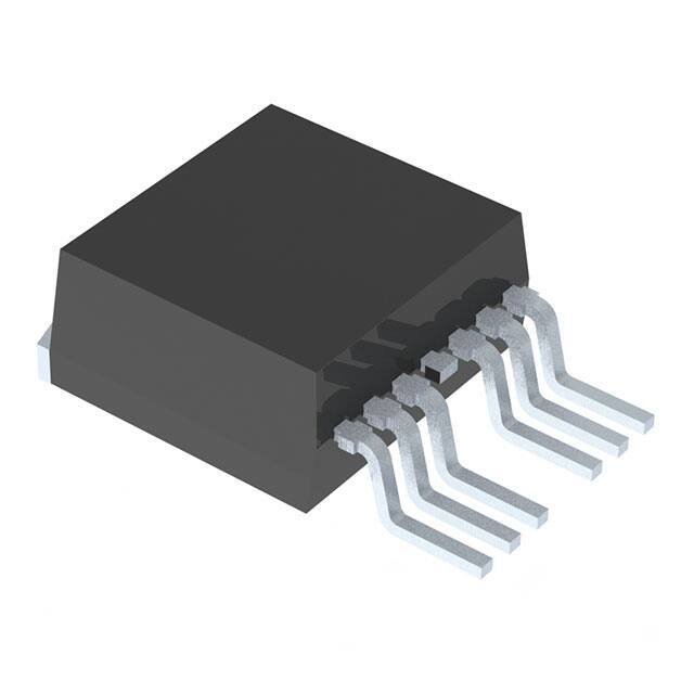
TO263-7L
• Overvoltage protection (including load dump)
• Loss of ground protection
• Loss of supply protection (with external diode for charged
inductive load)
1
• Very low standby current
7
• Fast demagnetization of inductive loads
TO220-7L
• ESD protection
• Optimized static electromagnetic compatibility
• Diagnostic function - Proportional load current sense (with
defined fault signal in case of overload operation, over temperature shutdown and/or short circuit shutdown)
• Qualified to AEC
Typical Applications
• Power switch with current sense diagnostic feedback for DC
grounded loads
• All types of resistive, inductive, and capacitive loads
• Replace electromechanical relays, fuses and discrete circuits
Ordering Information
Part Number
Package
Operating
Temperature
FDBS09H04A_F085A
TO263-7L
-40 C - 150 C
Eco Status
RoHS
Packing Method
Tape & Reel
For Fairchild’s definition of “green” Eco Status, please visit: http://www.fairchildsemi.com/company/green/rohs_green.html.
©2011 Fairchild Semiconductor Corporation
FDBS09H04A_F085A/FDPS09H04A_F085A
1
www.fairchildsemi.com
FDBS09H04A_F085A/FDPS09H04A_F085A Smart High Side Switch
April 2012
�Rbb
Charge
Pump
Voltage
Source
Current
Limit
Vbb
4
Gate
Protection
1
High-side Driver
OUT 2
6
7
SCIS
Input / Output
IN ESD & OVP
3
Protection
5
UVLO
&
Control
Logic
IS
Temp.
Sense
Current
Sense
Overload
Detection
Output Voltage
Detection
Pin Definitions
Pin Number
Pin Name
I/O
1
OUT
A
Output to loads; Pins 1, 2, 6 and 7 must be externally shorted
2
OUT
A
Output to loads; Pins 1, 2, 6 and 7 must be externally shorted
3
IN
A
Input; Activates the power switch if shorted to ground
4
Vbb
P
Supply Voltage; Pin 4 and tab are internally shorted
5
IS
A
Sense Output, Diagnostic feedback; Provides at normal operation a sense
current proportional to the load current; in case of overload, over temperature and/or short circuit a defined current is provided
6
OUT
A
Output to loads; Pins 1, 2, 6 and 7 must be externally shorted
7
OUT
A
Output to loads; Pins 1, 2, 6 and 7 must be externally shorted
©2011 Fairchild Semiconductor Corporation
FDBS09H04A_F085A/FDPS09H04A_F085A
Pin Function Description
2
www.fairchildsemi.com
FDBS09H04A_F085A/FDPS09H04A_F085A Smart High Side Switch
Block Diagram
�At Tj=25C unless otherwise specified.
Parameter
Symbol
Values
Unit
Supply voltage
Vbb
38
V
Supply voltage for full short circuit protection 1)
Vbb
30
V
VLoadDump 2)
45
V
Load dump protection VLoadDump = UA + VS, UA=13.5V
RI=2, RL=1, td=400ms, IN=Low or High
IL
Self-limited
A
Tj
Tstg
-40 - 150
-55 - 150
C
C
Ptot
81
W
EAS
388
mJ
Load current (short-circuit current)
Operating temperature range
Storage temperature range
Power Dissipation (DC)
3)
Inductive load switch-off energy dissipation
Single pulse, IL=12.5A, L=5mH, Vbb=12V, Tj=150C
Electrostatic discharge capability (ESD)
(Human Body Model)
IS
VESD
2
KV
IN
VESD
2
KV
VBB, Output
VESD
5
KV
IIN
IIS
+15, -120
+15, -120
mA
dVbIN / dt
self-limited
20
V/us
Current through input pin (DC)
Current through current sense pin (DC)
Input voltage slew rate Vbb 16V 4)
Notes:
1) Short circuit is defined as a combination of remaining resistances and inductances. See schematic on page11.
2) VLoad dump is setup without the DUT connected to the generator.
3) See also diagram on page 11.
4) See also on page 7. Slew rate limitation can be achieved by means of using a series resistor RIN in the input path. This resistor is also required for reverse operation. See also
page 10.
©2011 Fairchild Semiconductor Corporation
FDBS09H04A_F085A/FDPS09H04A_F085A
3
www.fairchildsemi.com
FDBS09H04A_F085A/FDPS09H04A_F085A Smart High Side Switch
Absolute Maximum Ratings
�At Tj=25C, Vbb=12V unless otherwise specified.
Parameter
Symbol
Conditions
RthJC 5)
RthJA
(junction to case)
(junction to ambient)
device on PCB 6), SMD version only
Min. Typ. Max. Unit
Thermal Characteristics
Thermal resistance
-
0.6
70
35
0.8
45
K/W
Load Switching Capability and Characteristics
On-state resistance
(pin 3 to pins 1, 2, 6, 7)
RON
VIN=0, Vbb=5.5V, IL=10A, Tj=25C
VIN=0, Vbb=5.5V, IL=10A, Tj=150C
VIN=0, Vbb=12V, IL=10A, Tj=25C
VIN=0, Vbb=12V, IL=10A, Tj=150C
-
5.5
10
5.5
10
9
15
9
15
m
VON(NL)
Tj=-40 - 150C
-
35
65
mV
IL(ISO)
ISO Proposal7): VON 1V, typ Tj = -40 - 150C
3.5
5.2
7.5
mA
KILIS
IIN=0(e.g. during deenergizing of induc-
tive loads)
Sense current under fault conditions17)
Sense saturation current
Fault-sense signal delay after input
current positive slope
Current sense leakage current
IIS,lim
VON < 1V, typ Tj = -40 - 150C
3.5
5.8
8.5
mA
tdelay(fault)
VON > 1V, typ Tj = -40 - 150C
350
500
650
us
IIS(LL)
IIN = 0
-
0
0.5
uA
Current sense offset current
IIS(LH)
VIN = 0, IL 20A, Tj = -40 - 150C
-
300
650
us
Current sense settling timeduring on
condition 18)
tslc(IS)
IL =10 --> 20A ,Tj=-40 ~ 150C
-
50
100
us
Overvoltage protection
VZ,IS
Ibb = 15mA, Tj = -40 - 150C
42.5
47.3
-
V
Required current capability of input
switch
IIN(on)
Tj = -40 - 150C
-
1.5
3.0
mA
Input current for turn-off
IIN(off)
Tj = -40 - 150C
-
-
15
uA
Input
Notes:
16) See also Figures 4.x and 6.x on page 15 and 16.
17) Fault conditions are overload during on (i.e. VON>1V typ.), over temperature and short circuit; see also truth table on page 7.
18) Not subject to production test, specified by design.
©2011 Fairchild Semiconductor Corporation
FDBS09H04A_F085A/FDPS09H04A_F085A
6
www.fairchildsemi.com
FDBS09H04A_F085A/FDPS09H04A_F085A Smart High Side Switch
Electrical Characteristics
�FDBS09H04A_F085A/FDPS09H04A_F085A Smart High Side Switch
Application Information
1. Truth Table
Sense current under fault conditions
Output Level
Current Sense
Normal operation
Input Current Level
L
H
L
H
0 (IIS(LL))
nominal
Overload 19)
L
H
L
H
0 (IIS(LL))
IIS,fault
Short circuit to GND 20)
L
H
L
L
0 (IIS(LL))
IIS,fault
Over temperature
L
H
L
L
0 (IIS(LL))
IIS,fault
Short circuit to Vbb
L
H
H
H
0 (IIS(LL))
< nominal 21)
Open load
L
H
Z
H
0 (IIS(LL))
0 (IIS(LH))
L = “ Low “ Level, Z = High impedance, potential depends on external circuit, H = “HIGH” Level
2.Terms
Ibb
VON
VbIN
4
VbIS
V bb
Vbb
3
IN
OUT
IL
1,2,6,7
IS
R IN
IIN
IIS
VOUT
VIN
5
VIS
R IS
Notes:
19) Overload is detected at the following condition: 1V (typ.) < VON < 3.5V (typ.). See also page 10.
20) Short Circuit is detected at the following condition: VON > 3.5V (typ.). See also page 11.
21) Low ohmic short to Vbb may reduce the output current IL and therefore also the sense current IIS.
©2011 Fairchild Semiconductor Corporation
FDBS09H04A_F085A/FDPS09H04A_F085A
7
www.fairchildsemi.com
�3.1 Input circuit (ESD protection)
Vbb
VZ,IN
VbIN
ZD
Rbb
VIN
IIN
ESD zener diode: 47.3V typ., max 15mA
3.2 Current sense output
Vbb
Rbb
VZ,IS
IIS,fault
IS
IIS
VIS
RIS
VZ,IS = 47.3V ( typ.), RIS = 1K nominal (or 1K /n, if n devices are connected in parallel). IS = IL/kilis can be only driven by the internal circuit as long as VOUT - VIS > 5V. Therefore RIS should be less than
Vbb
– 5V------------------------8.5mA
Note: For large values of RIS the voltage VIS can reach almost Vbb. See also over voltage protection. If you don't use the current
sense output in your application, you can leave it open.
3.3 Inductive and over voltage output clamp
Vbb
VZ1
VON
OUT
VON is clamped to VON(CL) = 41.5V typical
©2011 Fairchild Semiconductor Corporation
FDBS09H04A_F085A/FDPS09H04A_F085A
8
www.fairchildsemi.com
FDBS09H04A_F085A/FDPS09H04A_F085A Smart High Side Switch
3. Detailed Function Blocks
�Vbb
VZ,IN VZ,IS
Rbb
RIN
Logic
IN
OUT
IS
RV
RIS
VZ,VIS
Rbb = 85 typ., VZ,IN = VZ,IS = 47.3V typ., RIS = 1K nominal. Note that when over voltage exceeds 47.3V typ. a voltage above 5V
can occur between IS and GND, if RV, VZ,VIS are not used.
3.5 Reverse battery protection
Vbb
Rbb
RIN
IN
Logic
OUT
IS
RL
RIS
RIS typ. 1K Add RIN for reverse battery protection in application with Vbb above 16V;
1 - ------1
0.082A
-------+ - --------------------------R IN R is V bb – 9V
To minimize power dissipation at reverse battery operation, the overall current into the IN and IS pin should be about 82mA. The current can be provided by using a small signal diode D in parallel to the input switch, by using a MOSFET input switch or by properly
adjusting the current through RIS. Since the current via Rbb generates additional heat in the device, this has to be taken into account
in the overall thermal consideration.
©2011 Fairchild Semiconductor Corporation
FDBS09H04A_F085A/FDPS09H04A_F085A
9
www.fairchildsemi.com
FDBS09H04A_F085A/FDPS09H04A_F085A Smart High Side Switch
3.4 Overvoltage protection of logic part
�Vbb
+
OUT
Vbb
-
IN
-IL
IS
VOUT
IIS
+
=
VIS
VIN
-
RIS
The device can be operated in inverse load current mode (VOUT > Vbb > 0V). The current sense feature is not available during this
kind of operation (IIS = 0). In case of inverse operation the intrinsic drain source diode is eventually conducting resulting in considerably increased power dissipation. The transition from inverse to forward mode can result in a delayed switch on.
Note: Temperature protection during inverse load current operation is not possible!
3.7 Vbb disconnect with energized inductive load
Vbb
IN
OUT
VD
Vbb
IS
VZL
Provide a current path with load current capability by using a diode, a Z-diode, or a varistor(VZL+ VD < 38V if RIN = 0). For higher
clamp voltages currents at IN and IS have to be limited to 120 mA.
3.8 Overload detection
Vbb
VON
Detection
Logic
OUT
Fault Condition: VON > 1V typ.
©2011 Fairchild Semiconductor Corporation
FDBS09H04A_F085A/FDPS09H04A_F085A
10
www.fairchildsemi.com
FDBS09H04A_F085A/FDPS09H04A_F085A Smart High Side Switch
3.6 Inverse load current operation
�FDBS09H04A_F085A/FDPS09H04A_F085A Smart High Side Switch
3.9 Short circuit
Vbb
5uH
IN
OUT
10mohm
LSC
IS
Vbb
=
IIN
-iL(t)
RSC
SC
RIS
ZL
Fault Condition: VON > VON(SC) (3.5V typ.) and t > td(SC) (typ. 650us)
Short circuit is a combination of primary and secondary impedances and resistances.
3.10 Inductive load switch-off energy dissipation
Ebb
EAS
ELoad
Vbb
Vbb
IN
=
-iL(t)
OUT
EL
IS
L
{R
ZL
RIS
IIN
L
ER
Energy stored in load inductance:
EL = 1 2 L IL
2
While demagnetizing load inductance, the energy dissipated in MOSFET is
E AS = E bb + E L – E R =
VON CL iL t dt
with an approximate solution for RL > 0 Vout(CL) = VoN(CL) - Vbb:
IL L
IL RL
E AS = --------------- V ON CL ln 1 + -----------------------------
2 RL
V OUT CL
©2011 Fairchild Semiconductor Corporation
FDBS09H04A_F085A/FDPS09H04A_F085A
11
www.fairchildsemi.com
�FDBS09H04A_F085A/FDPS09H04A_F085A Smart High Side Switch
3.11 Maximum allowable load inductance for a single switch off
L=f(IL); Tj = 150C, Vbb=12V, RL = 0
1000
L[mH]
100
10
1
0.1
0.01
©2011 Fairchild Semiconductor Corporation
1
FDBS09H04A_F085A/FDPS09H04A_F085A
10
12
I_L[A]
100
www.fairchildsemi.com
�VBB
Control
IN
Rin
IS
Diagnosis
OUT
Ris
M
Vbb
Rbb
*1
RIN
1K
On
Off
Output
*3
R1
4
IN
Bat
OUT
3
100
C
1,2,6,7
IS
5
R2
R3
MCU
*2
R4
3K
Load
ADC
*1
5.1V
RIS
1K
1) Ris and Rin is recommended as 1k
2) Put diode or capacitor between load to protect device or to remove noise.
3) For reverse battery protection function, R1 should be used less than 120at -18V.
©2011 Fairchild Semiconductor Corporation
FDBS09H04A_F085A/FDPS09H04A_F085A
13
www.fairchildsemi.com
FDBS09H04A_F085A/FDPS09H04A_F085A Smart High Side Switch
Typical Application Circuit
�IIN
IIN
VOUT
VOUT
90%
ton
dV/dtoff
dV/dton
toff
10%
IL
IL
Load1
Tslc(IS)
Load2
IIs
IIs
t
Tson(IS)
t
Tsoff(IS)
Figure 2a. Switching motors and lamps
As long as VbIS < VZ,IS the sense current will never
exceed IIS,fault and/or IIS,lim
Figure 1a. Switching a resistive load,
change of load current in ON-condition
The sense signal is not valid during a settling time
after turn-on/off and after change of load current
IIN
IL(SC)
[A]
120
100
VOUT
80
VON(CL)
60
40
IL
20
VON
IIs
0
t
Figure 2b. Switching an inductive load
©2011 Fairchild Semiconductor Corporation
FDBS09H04A_F085A/FDPS09H04A_F085A
10
20
30
[V]
Figure 3a. Typical current limitation characteristic
In case of VON > VON(SC)(typ.3.5V) the device will
be switched off by internal short circuit detection
14
www.fairchildsemi.com
FDBS09H04A_F085A/FDPS09H04A_F085A Smart High Side Switch
Timing Diagrams
�IL
IL
VON > VON(SC)
Td(SC2)
td(SC1)
VON
tm
IIs
1V typ
IIS,fault
tdelay(fault)
tdealy(fault)
t
IIs
Figure 3b. Short circuit type one:
shut down by short circuit detection, reset by IIN=0
IIS,fault
IL/KiLiS
t
Shut down remains latched until next reset via input
Figure 3c. Short circuit type two:
shut down by short circuit detection, reset by IIN=0
IIN
IIN
IIS
VOUT
IIS,fault
IL
Vbb-VOUT
Auto
Restart
VON=1V typ.
RON*IL,lim
Is
Tj
t
t
IL/kilis
Figure 4a. Over temperature Reset if Tj < Tjt
©2011 Fairchild Semiconductor Corporation
FDBS09H04A_F085A/FDPS09H04A_F085A
IIS,lim
IIS,fault
Figure 4b. Overload Reset if Tj < Tjt
15
www.fairchildsemi.com
FDBS09H04A_F085A/FDPS09H04A_F085A Smart High Side Switch
IIN
IIN
�IIS
4
IIS,Lim
VIN = 0
3
VON(CL)
Dynamic,short
Undervoltage
not below
2
IL,Lim
VbIN(u)
1
IL(min)
IIN = 0
IIS(LH)
Vbb
0
VbIN(u) Vbb(ucp)
VON(CL)
0
Figure 5. Under voltage restart of charge pump and
over voltage clamp
10
IL
20
30
40
50 [A]
Figure 6a. Current sense versus load current
[V]
0.1
VON
kLILIS
30000
0.05
20000
10000
IL
0
5
10
15
20
25
30
IL
[A]
2
FDBS09H04A_F085A/FDPS09H04A_F085A
6
8
10
12
14
[A]
Figure 7. Output voltage drop versus load current
Figure 6b. Current sense ratio
©2011 Fairchild Semiconductor Corporation
4
16
www.fairchildsemi.com
FDBS09H04A_F085A/FDPS09H04A_F085A Smart High Side Switch
[mA]
VOUT
�FDBS09H04A_F085A/FDPS09H04A_F085A Smart High Side Switch
Package Dimensions
©2011 Fairchild Semiconductor Corporation
FDBS09H04A_F085A/FDPS09H04A_F085A
17
www.fairchildsemi.com
�FDBS09H04A_F085A/FDPS09H04A_F085A Smart High Side Switch
©2011 Fairchild Semiconductor Corporation
FDBS09H04A_F085A/FDPS09H04A_F085A
18
www.fairchildsemi.com
�FDBS09H04A_F085A/FDPS09H04A_F085A Smart High Side Switch
©2011 Fairchild Semiconductor Corporation
FDBS09H04A_F085A/FDPS09H04A_F085A
19
www.fairchildsemi.com
�


 工商网监
湘ICP备2023018690号
工商网监
湘ICP备2023018690号
