ON Semiconductor
Is Now
To learn more about onsemi™, please visit our website at
www.onsemi.com
onsemi and and other names, marks, and brands are registered and/or common law trademarks of Semiconductor Components Industries, LLC dba “onsemi” or its affiliates and/or
subsidiaries in the United States and/or other countries. onsemi owns the rights to a number of patents, trademarks, copyrights, trade secrets, and other intellectual property. A listing of onsemi
product/patent coverage may be accessed at www.onsemi.com/site/pdf/Patent-Marking.pdf. onsemi reserves the right to make changes at any time to any products or information herein, without
notice. The information herein is provided “as-is” and onsemi makes no warranty, representation or guarantee regarding the accuracy of the information, product features, availability, functionality,
or suitability of its products for any particular purpose, nor does onsemi assume any liability arising out of the application or use of any product or circuit, and specifically disclaims any and all
liability, including without limitation special, consequential or incidental damages. Buyer is responsible for its products and applications using onsemi products, including compliance with all laws,
regulations and safety requirements or standards, regardless of any support or applications information provided by onsemi. “Typical” parameters which may be provided in onsemi data sheets and/
or specifications can and do vary in different applications and actual performance may vary over time. All operating parameters, including “Typicals” must be validated for each customer application
by customer’s technical experts. onsemi does not convey any license under any of its intellectual property rights nor the rights of others. onsemi products are not designed, intended, or authorized
for use as a critical component in life support systems or any FDA Class 3 medical devices or medical devices with a same or similar classification in a foreign jurisdiction or any devices intended for
implantation in the human body. Should Buyer purchase or use onsemi products for any such unintended or unauthorized application, Buyer shall indemnify and hold onsemi and its officers, employees,
subsidiaries, affiliates, and distributors harmless against all claims, costs, damages, and expenses, and reasonable attorney fees arising out of, directly or indirectly, any claim of personal injury or death
associated with such unintended or unauthorized use, even if such claim alleges that onsemi was negligent regarding the design or manufacture of the part. onsemi is an Equal Opportunity/Affirmative
Action Employer. This literature is subject to all applicable copyright laws and is not for resale in any manner. Other names and brands may be claimed as the property of others.
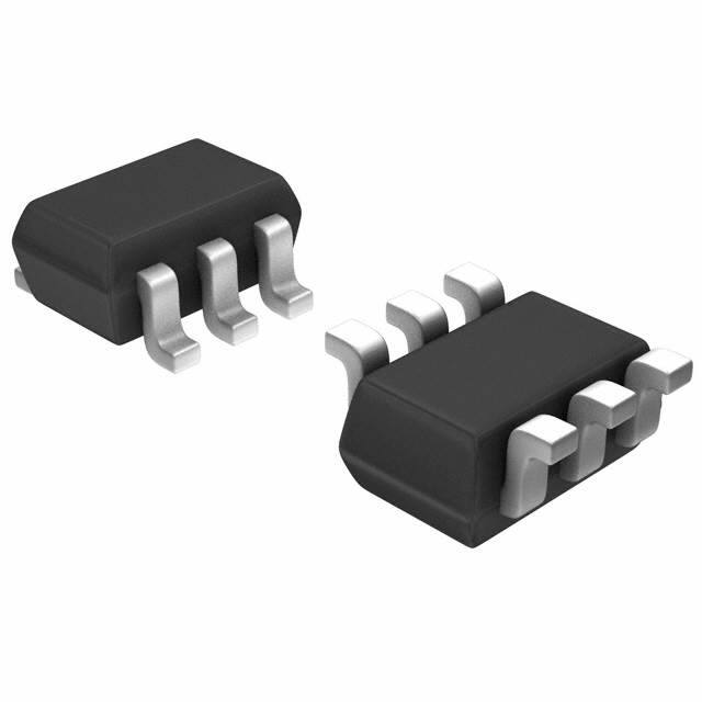
�Integrated Load Switch
General Description
This device is particularly suited for compact power
management in portable electronic equipment where 2.5V to 8V
input and 1.5A output current capability are needed. This load
switch integrates a small N-Channel power MOSFET (Q1) that
drives a large P-Channel power MOSFET (Q2) in one tiny
SC70-6 package.
Features
Max rDS(on) = 150mΩ at VGS = 4.5V, ID = –1.5A
Max rDS(on) = 195mΩ at VGS = 2.5V, ID = –1.3A
Max rDS(on) = 280mΩ at VGS = 1.8V, ID = –1.1A
Max rDS(on) = 480mΩ at VGS = 1.5V, ID = –0.9A
Applications
Control MOSFET (Q1) includes Zener protection for ESD
ruggedness ( >4KV Human body model)
Power management
Load switch
High performance trench technology for extremely low rDS(on)
Compact industry standard SC70-6 surface mount package
RoHS Compliant
Q2
Vin,R1
3
4
Equivalent Circuit
Vout,C1
IN
ON/OFF
5
R1,C1
6
Q1
2
Vout,C1
1
R2
VDROP
OUT
ON/OFF
Pin 1
SC70-6
See Application Circuit
MOSFET Maximum Ratings TA = 25°C unless otherwise noted
Parameter
Symbol
VIN
Gate to Source Voltage (Q2)
VON/OFF
Gate to Source Voltage (Q1)
ILoad
Load Current
TJ, TSTG
Units
V
–0.5 to 8
V
-Continuous
(Note 2)
1.5
-Pulsed
(Note 2)
6
(Note 1a)
0.36
(Note 1b)
0.3
Power Dissipation for Single Operation
PD
Ratings
±8
Operating and Storage Junction Temperature Range
A
W
–55 to +150
°C
Thermal Characteristics
RθJA
Thermal Resistance, Junction to Ambient Single operation
(Note 1a)
350
RθJA
Thermal Resistance, Junction to Ambient Single operation
(Note 1b)
415
°C/W
Package Marking and Ordering Information
Device Marking
.2L
Device
FDG6342L
©2008 Semiconductor Components Industries, LLC.
October-2017, Rev.2
Package
SC70-6
1
Reel Size
7’’
Tape Width
8mm
Quantity
3000units
Publication Order Number:
FDG6342L/D
FDG6342L Integrated Load Switch
FDG6342L
�Symbol
Parameter
Test Conditions
Min
Typ
Max
Units
–1
µA
Off Characteristics
BVIN
VIN Breakdown Voltage
ID = -250µA, VON/OFF = 0V
ILoad
Zero Gate Voltage Drain Current
VIN = -6.4V, VON/OFF = 0V
8
V
IFL
Leakage Current, Forward
VIN = 8V, VON/OFF = 0V
10
µA
IRL
Leakage Current, Reverse
VIN = –8V, VON/OFF = 0V
–10
µA
V
On Characteristics (note 2)
VON/OFF(th)
rDS(on)
Gate Threshold Voltage
VIN = VON/OFF, ID = -250µA
Static Drain to Source On Resistance (Q2)
Static Drain to Source On Resistance (Q1)
0.8
1.5
VIN = 4.5V, ID = –1.5A
0.65
125
150
VIN = 2.5V, ID = –1.3A
150
195
VIN = 1.8V, ID = –1.1A
200
280
VIN = 1.5V, ID = –0.9A
250
480
VIN = 4.5V, ID = 0.4A
2.6
4.0
VIN = 2.7V, ID = 0.2A
3.3
5.0
mΩ
Ω
Drain-Source Diode Characteristics
IS
Maximum Continuous Drain to Source Diode Forward Current
VSD
Source to Drain Diode Forward Voltage
VON/OFF = 0V, IS = –0.25A (Note 2)
–0.6
–0.25
A
–1.2
V
NOTES:
1. RθJA is determined with the device mounted on a 1in2 pad 2 oz copper pad on a 1.5 x 1.5 in. board of FR-4 material. RθJC is guaranteed by design while RθJA is determined by
the user's board design.
a. 350°C/W when mounted on a
1 in2 pad of 2 oz copper .
2. Pulse Test: Pulse Width < 300µs, Duty cycle < 2.0%.
FDG6342LLoad Switch Application circuit
Q2
IN
OUT
C1
R1
Q1
LOAD
ON/OFF
R2
External Component Recommendation:
For additional in-rush current control, R2 and C1 can be added. For more information, see application note AN1030
www.onsemi.com
2
b. 415°C/W when mounted on
a minimum pad of 2 oz copper.
FDG6342L Integrated Load Switch
Electrical Characteristics TJ = 25°C unless otherwise noted
�0.5
0.5
VIN = -1.5V
VON/OFF = 1.5-8V
PW = 300µs, D < 2%
0.4
TJ = 125oC
0.3
-VDROP, (V)
-VDROP, (V)
0.4
VIN = -1.8V
VON/OFF = 1.5-8V
PW = 300µs, D < 2%
TJ = 25oC
0.2
0.1
TJ = 125oC
0.3
TJ = 25oC
0.2
0.1
0.0
0.0
0.4
0.8
1.2
1.6
0.0
0.0
2.0
0.5
1.0
-IL, (A)
Figure 1. Conduction Voltage Drop
Variation with Load Current.
2.5
3.0
0.5
VIN = -2.5V
VON/OFF = 1.5-8V
PW = 300µs, D < 2%
TJ
VIN = -4.5V
VON/OFF = 1.5-8V
PW = 300µs, D < 2%
0.4
= 125oC
-VDROP, (V)
0.4
-VDROP, (V)
2.0
Figure 2. Conduction Voltage Drop
Variation with Load Current.
0.5
0.3
TJ = 25oC
0.2
0.1
TJ = 125oC
0.3
TJ = 25oC
0.2
0.1
0.0
0.0
0.5
1.0
1.5
2.0
2.5
3.0
0.0
0.0
3.5
0.5
1.0
1.5
-IL, (A)
2.0
2.5
3.0
3.5
4.0
4.5
-IL, (A)
Figure 3. Conduction Voltage Drop
Variation with Load Current.
Figure 4. Conduction Voltage Drop
Variation with Load Current.
0.6
IL = -1.3A
VON/OFF = 1.5-8V
PW = 300µs, D < 2%
0.5
0.4
0.3
TJ = 125oC
0.2
TJ =
0.1
0.0
1.0
1.5
25oC
2.0
2.5
3.0
3.5
4.0
4.5
rDS(on), ON-RESISTANGE (Ω)
0.6
rDS(on), ON-RESISTANGE (Ω)
1.5
-IL, (A)
IL = -1.5A
VON/OFF = 1.5-8V
PW = 300µs, D < 2%
0.5
0.4
TJ = 125oC
0.3
0.2
0.1
TJ = 25oC
0.0
1.0
-VIN, INPUT VOLTAGE (V)
1.5
2.0
2.5
3.0
3.5
4.0
-VIN, INPUT VOLTAGE (V)
Figure 5. On-Resistance Variation
With Input Voltage
Figure 6. On-Resistance Variation
With Input Voltage
www.onsemi.com
3
4.5
FDG6342L Integrated Load Switch
Typical Characteristics TJ = 25°C unless otherwise noted
�FDG6342L Integrated Load Switch
Dimensional Outline and Pad Layout
Package drawings are provided as a service to customers considering ON Semiconductor components. Drawings may change in
any manner without notice. Please note the revision and/or date on the drawing and contact a ON Semiconductor representative to
verify or obtain the most recent revision. Package specifications do not expand the terms of ON Semiconductor’s worldwide terms
and conditions, specifically the warranty therein, which covers ON Semiconductor products.
www.onsemi.com
4
�ON Semiconductor and
are trademarks of Semiconductor Components Industries, LLC dba ON Semiconductor or its subsidiaries in the United States and/or other countries.
ON Semiconductor owns the rights to a number of patents, trademarks, copyrights, trade secrets, and other intellectual property. A listing of ON Semiconductor’s product/patent
coverage may be accessed at www.onsemi.com/site/pdf/Patent−Marking.pdf. ON Semiconductor reserves the right to make changes without further notice to any products herein.
ON Semiconductor makes no warranty, representation or guarantee regarding the suitability of its products for any particular purpose, nor does ON Semiconductor assume any liability
arising out of the application or use of any product or circuit, and specifically disclaims any and all liability, including without limitation special, consequential or incidental damages.
Buyer is responsible for its products and applications using ON Semiconductor products, including compliance with all laws, regulations and safety requirements or standards,
regardless of any support or applications information provided by ON Semiconductor. “Typical” parameters which may be provided in ON Semiconductor data sheets and/or
specifications can and do vary in different applications and actual performance may vary over time. All operating parameters, including “Typicals” must be validated for each customer
application by customer’s technical experts. ON Semiconductor does not convey any license under its patent rights nor the rights of others. ON Semiconductor products are not
designed, intended, or authorized for use as a critical component in life support systems or any FDA Class 3 medical devices or medical devices with a same or similar classification
in a foreign jurisdiction or any devices intended for implantation in the human body. Should Buyer purchase or use ON Semiconductor products for any such unintended or unauthorized
application, Buyer shall indemnify and hold ON Semiconductor and its officers, employees, subsidiaries, affiliates, and distributors harmless against all claims, costs, damages, and
expenses, and reasonable attorney fees arising out of, directly or indirectly, any claim of personal injury or death associated with such unintended or unauthorized use, even if such
claim alleges that ON Semiconductor was negligent regarding the design or manufacture of the part. ON Semiconductor is an Equal Opportunity/Affirmative Action Employer. This
literature is subject to all applicable copyright laws and is not for resale in any manner.
PUBLICATION ORDERING INFORMATION
LITERATURE FULFILLMENT:
Literature Distribution Center for ON Semiconductor
19521 E. 32nd Pkwy, Aurora, Colorado 80011 USA
Phone: 303−675−2175 or 800−344−3860 Toll Free USA/Canada
Fax: 303−675−2176 or 800−344−3867 Toll Free USA/Canada
Email: orderlit@onsemi.com
❖
© Semiconductor Components Industries, LLC
N. American Technical Support: 800−282−9855 Toll Free
USA/Canada
Europe, Middle East and Africa Technical Support:
Phone: 421 33 790 2910
Japan Customer Focus Center
Phone: 81−3−5817−1050
ON Semiconductor Website: www.onsemi.com
Order Literature: http://www.onsemi.com/orderlit
For additional information, please contact your local
Sales Representative
www.onsemi.com
�


 工商网监
湘ICP备2023018690号
工商网监
湘ICP备2023018690号
