FGD3040G2-F085C
FGB3040G2-F085C
EcoSPARK� 2 Ignition IGBT
300 mJ, 400 V, N−Channel Ignition IGBT
Features
•
•
•
•
www.onsemi.com
SCIS Energy = 300 mJ at TJ = 25°C
Logic Level Gate Drive
AEC−Q101 Qualified and PPAP Capable
These Devices are Pb−Free and are RoHS Compliant
COLLECTOR
Applications
• Automotive Ignition Coil Driver Circuits
• High Current Ignition System
• Coil on Plug Application
R1
GATE
R2
EMITTER
MAXIMUM RATINGS (TJ = 25°C unless otherwise noted)
Symbol
Parameter
Value
Unit
BVCER
Collector to Emitter Breakdown
Voltage (IC = 1 mA)
400
V
BVECS
Emitter to Collector Voltage − Reverse
Battery Condition (IC = 10 mA)
28
V
ESCIS25
ISCIS = 14.2 A, L = 3.0 mHy,
RGE = 1 KW, TC = 25°C (Note 1)
300
mJ
170
mJ
Collector Current Continuous
at VGE = 5.0 V, TC = 25°C
41
A
IC110
Collector Current Continuous
at VGE = 5.0 V, TC = 110°C
25.6
A
VGEM
Gate to Emitter Voltage Continuous
±10
V
PD
Power Dissipation Total, TC = 25°C
150
W
1
W/°C
−55 to +175
°C
Lead Temperature for Soldering
Purposes (1/8” from case for 10 s)
300
°C
TPKG
Reflow Soldering according to
JESD020C
260
°C
ESD
HBM−Electrostatic Discharge Voltage
at 100 pF, 1500 W
4
kV
CDM−Electrostatic Discharge Voltage
at 1 W
2
kV
ESCIS150 ISCIS = 10.8 A, L = 3.0 mHy,
RGE = 1 KW, TC = 150°C (Note 2)
IC25
Power Dissipation Derating, TC > 25°C
TJ, TSTG Operating Junction and Storage
Temperature
TL
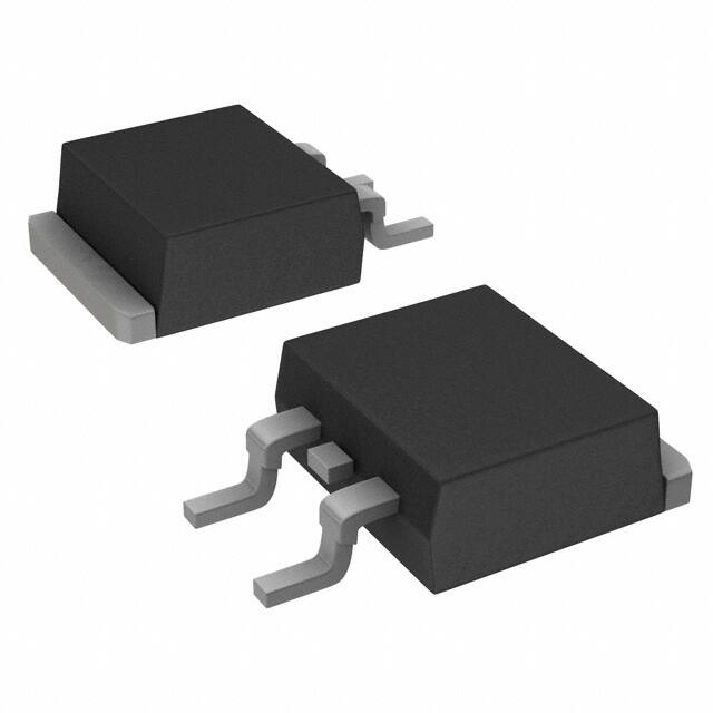
D2PAK−3
CASE 418AJ
DPAK3
CASE 369AS
MARKING DIAGRAM
AYWW
XXX
XXXXXG
A
Y
WW
XXXX
G
= Assembly Location
= Year
= Work Week
= Device Code
= Pb−Free Package
ORDERING INFORMATION
See detailed ordering and shipping information on page 2
of this data sheet.
Stresses exceeding those listed in the Maximum Ratings table may damage the
device. If any of these limits are exceeded, device functionality should not be
assumed, damage may occur and reliability may be affected.
1. Self clamped inductive Switching Energy (ESCIS25) of 300 mJ is based on
the test conditions that is starting TJ = 25°C, L = 3 mHy, ISCIS = 14.2 A,
VCC = 100 V during inductor charging and VCC = 0 V during time in clamp.
2. Self Clamped inductive Switching Energy (ESCIS150) of 170 mJ is based on
the test conditions that is starting TJ = 150°C, L = 3mHy, ISCIS = 10.8 A,
VCC = 100 V during inductor charging and VCC = 0 V during time in clamp.
© Semiconductor Components Industries, LLC, 2016
April, 2019 − Rev. 1
1
Publication Order Number:
FGX3040G2−F085C//D
�FGD3040G2−F085C
THERMAL RESISTANCE RATINGS
Characteristic
Symbol
Max
Units
RqJC
1
°C/W
Junction−to−Case – Steady State (Drain)
ELECTRICAL CHARACTERISTICS (TJ = 25°C unless otherwise specified)
Symbol
Parameter
Test Conditions
Min
Typ.
Max.
Units
OFF CHARACTERISTICS
BVCER
Collector to Emitter Breakdown
Voltage
ICE = 2 mA, VGE = 0 V,
RGE = 1 kW,
TJ = −40 to 150°C
370
400
430
V
BVCES
Collector to Emitter Breakdown
Voltage
ICE = 10 mA, VGE = 0 V,
RGE = 0,
TJ = −40 to 150°C
390
420
450
V
BVECS
Emitter to Collector Breakdown
Voltage
ICE = −75 mA, VGE = 0 V,
TJ = 25°C
28
−
−
V
BVGES
Gate to Emitter Breakdown Voltage
IGES = ±2 mA
±12
±14
−
V
ICER
Collector to Emitter Leakage Current
VCE = 175 V
RGE = 1 kW
TJ = 25°C
−
−
25
mA
TJ = 150°C
−
−
1
mA
VEC = 24 V
TJ = 25°C
−
−
1
mA
TJ = 150°C
−
−
40
−
120
−
W
10K
−
30K
W
IECS
Emitter to Collector Leakage Current
R1
Series Gate Resistance
R2
Gate to Emitter Resistance
ON CHARACTERISTICS
VCE(SAT)
Collector to Emitter Saturation
Voltage
ICE = 6 A, VGE = 4 V, TJ = 25°C
−
1.15
1.25
V
VCE(SAT)
Collector to Emitter Saturation
Voltage
ICE = 10 A, VGE = 4.5 V, TJ = 150°C
−
1.35
1.50
V
VCE(SAT)
Collector to Emitter Saturation
Voltage
ICE = 15 A, VGE = 5 V, TJ = 150°C
−
1.68
1.85
V
DYNAMIC CHARACTERISTICS
QG(ON)
Gate Charge
ICE = 10 A, VCE = 12 V, VGE = 5 V
VGE(TH)
Gate to Emitter Threshold Voltage
ICE = 1 mA
VCE = VGE
Gate to Emitter Plateau Voltage
VCE = 12 V, ICE = 10 A
VGEP
−
21
−
nC
TJ = 25°C
1.3
1.5
2.2
V
TJ = 150°C
0.75
1.2
1.8
−
2.8
−
V
VCE = 14 V, RL = 1 W,
VGE = 5 V, RG = 470 W,
TJ = 25°C
−
0.9
4
ms
−
1.9
7
VCE = 300 V, L = 1 mH,
VGE = 5 V, RG = 470 W,
ICE = 6.5 A, TJ = 25°C
−
4.8
10
−
2.0
15
SWITCHING CHARACTERISTICS
td(ON)R
trR
td(OFF)L
tfL
Current Turn−On Delay
Time−Resistive
Current Rise Time−Resistive
Current Turn−Off Delay
Time−Inductive
Current Fall Time−Inductive
Product parametric performance is indicated in the Electrical Characteristics for the listed test conditions, unless otherwise noted. Product
performance may not be indicated by the Electrical Characteristics if operated under different conditions.
PACKAGE MARKING AND ORDERING INFORMATION
Device
Package
Shipping†
FGD3040G2−F085C
DPAK
(Pb−Free)
2500 Units / Tape & Reel
FGB3040G2−F085C
D2PAK
(Pb−Free)
800 Units / Tape & Reel
†For information on tape and reel specifications, including part orientation and tape sizes, please refer to our Tape and Reel Packaging
Specifications Brochure, BRD8011/D.
www.onsemi.com
2
�FGD3040G2−F085C
TYPICAL CHARACTERISTICS
Figure 1. Self Clamped Inductive Switching
Current vs. Time in Clamp
Figure 2. Self Clamped Inductive
Switching Current vs. Inductance
Figure 4. Collector to Emitter On−State Voltage
vs. Junction Temperature
Figure 3. Collector to Emitter On−State Voltage
vs. Junction Temperature
Figure 5. Collector to Emitter On−State Voltage
vs. Collector Current
Figure 6. Collector to Emitter On−State Voltage
vs. Collector Current
www.onsemi.com
3
�FGD3040G2−F085C
TYPICAL CHARACTERISTICS (continued)
Figure 7. Collector to Emitter On−State Voltage
vs. Collector Current
Figure 8. Transfer Characteristics
Figure 10. Gate Charge
Figure 9. DC Collector Current vs. Case
Temperature
Figure 11. Threshold Voltage vs. Junction
Temperature
Figure 12. Leakage Current vs. Junction
Temperature
www.onsemi.com
4
�FGD3040G2−F085C
TYPICAL CHARACTERISTICS (continued)
Figure 13. Switching Time vs. Junction Temperature
Figure 14. Capacitance vs. Collector to Emitter
Figure 15. Break Down Voltage vs. Series Resistance
Figure 16. IGBT Normalized Transient Thermal Impedance, Junction to Case
www.onsemi.com
5
�FGD3040G2−F085C
TEST CIRCUIT AND WAVEFORMS
Figure 17. Inductive Switching Test Circuit
Figure 18. tON and tOFF Switching Test Circuit
Figure 19. Energy Test Circuit
Figure 20. Energy Waveforms
ECOSPARK is registered trademark of Semiconductor Components Industries, LLC (SCILLC) or its subsidiaries in the United States and/or other countries.
www.onsemi.com
6
�MECHANICAL CASE OUTLINE
PACKAGE DIMENSIONS
DPAK3 (TO−252 3 LD)
CASE 369AS
ISSUE O
DOCUMENT NUMBER:
DESCRIPTION:
98AON13810G
DPAK3 (TO−252 3 LD)
DATE 30 SEP 2016
Electronic versions are uncontrolled except when accessed directly from the Document Repository.
Printed versions are uncontrolled except when stamped “CONTROLLED COPY” in red.
PAGE 1 OF 1
ON Semiconductor and
are trademarks of Semiconductor Components Industries, LLC dba ON Semiconductor or its subsidiaries in the United States and/or other countries.
ON Semiconductor reserves the right to make changes without further notice to any products herein. ON Semiconductor makes no warranty, representation or guarantee regarding
the suitability of its products for any particular purpose, nor does ON Semiconductor assume any liability arising out of the application or use of any product or circuit, and specifically
disclaims any and all liability, including without limitation special, consequential or incidental damages. ON Semiconductor does not convey any license under its patent rights nor the
rights of others.
© Semiconductor Components Industries, LLC, 2019
www.onsemi.com
�MECHANICAL CASE OUTLINE
PACKAGE DIMENSIONS
D2PAK−3 (TO−263, 3−LEAD)
CASE 418AJ
ISSUE F
SCALE 1:1
GENERIC MARKING DIAGRAMS*
XX
XXXXXXXXX
AWLYWWG
IC
DOCUMENT NUMBER:
DESCRIPTION:
XXXXXXXXG
AYWW
Standard
98AON56370E
AYWW
XXXXXXXXG
AKA
Rectifier
XXXXXX
XXYMW
SSG
DATE 11 MAR 2021
XXXXXX = Specific Device Code
A
= Assembly Location
WL
= Wafer Lot
Y
= Year
WW
= Work Week
W
= Week Code (SSG)
M
= Month Code (SSG)
G
= Pb−Free Package
AKA
= Polarity Indicator
*This information is generic. Please refer to
device data sheet for actual part marking.
Pb−Free indicator, “G” or microdot “ G”,
may or may not be present. Some products
may not follow the Generic Marking.
Electronic versions are uncontrolled except when accessed directly from the Document Repository.
Printed versions are uncontrolled except when stamped “CONTROLLED COPY” in red.
D2PAK−3 (TO−263, 3−LEAD)
PAGE 1 OF 1
ON Semiconductor and
are trademarks of Semiconductor Components Industries, LLC dba ON Semiconductor or its subsidiaries in the United States and/or other countries.
ON Semiconductor reserves the right to make changes without further notice to any products herein. ON Semiconductor makes no warranty, representation or guarantee regarding
the suitability of its products for any particular purpose, nor does ON Semiconductor assume any liability arising out of the application or use of any product or circuit, and specifically
disclaims any and all liability, including without limitation special, consequential or incidental damages. ON Semiconductor does not convey any license under its patent rights nor the
rights of others.
© Semiconductor Components Industries, LLC, 2018
www.onsemi.com
�onsemi,
, and other names, marks, and brands are registered and/or common law trademarks of Semiconductor Components Industries, LLC dba “onsemi” or its affiliates
and/or subsidiaries in the United States and/or other countries. onsemi owns the rights to a number of patents, trademarks, copyrights, trade secrets, and other intellectual property.
A listing of onsemi’s product/patent coverage may be accessed at www.onsemi.com/site/pdf/Patent−Marking.pdf. onsemi reserves the right to make changes at any time to any
products or information herein, without notice. The information herein is provided “as−is” and onsemi makes no warranty, representation or guarantee regarding the accuracy of the
information, product features, availability, functionality, or suitability of its products for any particular purpose, nor does onsemi assume any liability arising out of the application or use
of any product or circuit, and specifically disclaims any and all liability, including without limitation special, consequential or incidental damages. Buyer is responsible for its products
and applications using onsemi products, including compliance with all laws, regulations and safety requirements or standards, regardless of any support or applications information
provided by onsemi. “Typical” parameters which may be provided in onsemi data sheets and/or specifications can and do vary in different applications and actual performance may
vary over time. All operating parameters, including “Typicals” must be validated for each customer application by customer’s technical experts. onsemi does not convey any license
under any of its intellectual property rights nor the rights of others. onsemi products are not designed, intended, or authorized for use as a critical component in life support systems
or any FDA Class 3 medical devices or medical devices with a same or similar classification in a foreign jurisdiction or any devices intended for implantation in the human body. Should
Buyer purchase or use onsemi products for any such unintended or unauthorized application, Buyer shall indemnify and hold onsemi and its officers, employees, subsidiaries, affiliates,
and distributors harmless against all claims, costs, damages, and expenses, and reasonable attorney fees arising out of, directly or indirectly, any claim of personal injury or death
associated with such unintended or unauthorized use, even if such claim alleges that onsemi was negligent regarding the design or manufacture of the part. onsemi is an Equal
Opportunity/Affirmative Action Employer. This literature is subject to all applicable copyright laws and is not for resale in any manner.
PUBLICATION ORDERING INFORMATION
LITERATURE FULFILLMENT:
Email Requests to: orderlit@onsemi.com
onsemi Website: www.onsemi.com
◊
TECHNICAL SUPPORT
North American Technical Support:
Voice Mail: 1 800−282−9855 Toll Free USA/Canada
Phone: 011 421 33 790 2910
Europe, Middle East and Africa Technical Support:
Phone: 00421 33 790 2910
For additional information, please contact your local Sales Representative
�


 工商网监
湘ICP备2023018690号
工商网监
湘ICP备2023018690号
