Battery Fuel Gauge LSI
[Smart LiB Gauge]
for 1-Cell Lithium-ion/
Polymer (Li+) with Low Power
2�mA Operation
LC709204F
www.onsemi.com
Overview
LC709204F is a Fuel Gauge for 1−Cell Lithium−ion/Polymer
batteries. It is part of our Smart LiB Gauge family of Fuel Gauges
which measure the battery RSOC (Relative State Of Charge) using its
unique algorithm called HG−CVR2. The HG−CVR2 algorithm
provides accurate RSOC information even under unstable conditions
(e.g. changes of battery; temperature, loading, aging and
self−discharge). An accurate RSOC contributes to the operating time
of portable devices. The Fuel Gauge (in other words, Gas Gauge,
Battery Monitor or Battery Gauge) feature of HG−CVR2 algorithm
makes LSI highly applicable in various application. The LSI can
immediately start battery measurement by setting a few parameters
after battery insertion. Learning cycles that make complicated
manufacturing process of applications can be avoided.
The LSI also supports battery safety by alarm functions and SOH
(State of Health) reporting to the application processor. The operating
consumption current is very low 2 mA and it is suitable for applications
such as wearables and 1 series N parallel batteries.
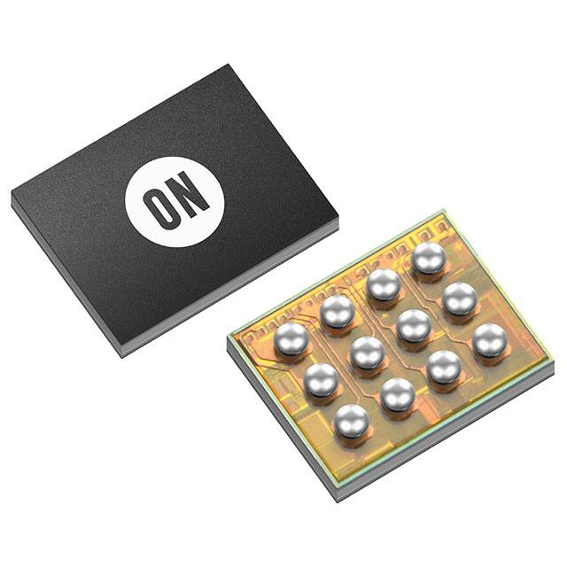
WLCSP12 1.48x1.91x0.51
CASE 567XE
MARKING DIAGRAM
204**
AWLYW
204**
A
WL
YW
Features
• HG−CVR2 Algorithm Technology
Small Footprint: No Need for Current Sensing Resistor
♦ Accurate RSOC of Aging Battery
♦ Stable Gauging by Automatic Convergence of Error
♦ Immediate Accurate Gauging after Battery Insertion
♦ Eliminates Learning Cycle
Low Power Consumption
♦ 2 mA Operational Mode Current
Improvement of the Battery Safety by Alarm Function
RSOC / Voltage / Temperature
Battery Lifetime Measurement
SOH / Cycle Count / Operating Time
Remaining Time Estimation
Time to Full / Time to Empty
Three Temperature Inputs
♦ Inputs to sense two NTC Thermistors
♦ Via I2C
Detection of Battery Operating Conditions
Charging / Discharging
Detection of Battery Insertion
I2C Interface (supported up to 400 kHz)
These Devices are Pb−Free, Halogen Free/BFR Free and are RoHS
Compliant
♦
•
•
•
•
•
•
•
•
•
© Semiconductor Components Industries, LLC, 2019
September, 2019 − Rev. 0
1
= 20401 (LC709204FXE−01TBG)
= Assembly Site
= Wafer Lot Number
= Assembly Start Week
ORDERING INFORMATION
See detailed ordering and shipping information on page 20 of
this data sheet.
Applications
•
•
•
•
•
Wearables / IoT Devices
Smartphones/PDA Devices
Digital Cameras
Portable Game Players
USB-related Devices
Publication Order Number:
LC709204F/D
�LC709204F
Application Circuit Example
ALARMB
VDD
1uF
T
TSENSE1
LC709204F
REG
VSS
ALARMB
2.2uF
Protection IC
SDA
PACK+
NTC Thermistor
SDA
Battery Pack
NTC Thermistor
SCL
SCL
TSENSE2
10 kW
10 kW
10 kW
Application
processor
System-VSS
System-VDD
Application
PACK-
Figure 1. Example of an Application Schematic using LC709204F
(The temperature is measured using TSENSE1 pin.)
Application
Battery Pack
REG
Thermistor -sense
2.2uF
PACK-
Figure 2. Example of an Application Schematic using LC709204F
(The Temperature is sent via I2C.)
www.onsemi.com
2
Protection IC
LC709204F
ALARMB
NTC Thermistor
ALARMB
SDA
T
TSENSE1
VSS
SDA
1uF
VDD
SCL
SCL
TSENSE2
10 kW
10 kW
10 kW
Application
processor
System-VSS
System-VDD
PACK+
�LC709204F
VDD
Regulator
REG
DRV
I 2C
Interface
SCL
SDA
TSENSE1
TSENSE2
Analog Front End
ALARMB
Look up table for
internal battery
impedance & OCV
Processing
unit
ADC
Timer
Internal
Thermistor
Power on reset
Figure 3. Block Diagram
ALARMB
TEST1
NF1
NF2
C1
C2
C3
C4
SCL
TEST2
B1
B2
B3
B4
SDA
VSS
REG
VDD
A1
A2
A3
A4
TSENSE2
TSENSE1
(Bottom View)
Figure 4. Pin Assignment
www.onsemi.com
3
TEST1
TEST2
VSS
�LC709204F
Table 1. PIN FUNCTION
WLCSP12
Name
I/O
Description
A1
SDA
I/O
I2C
B1
SCL
I/O
I2C Clock pin (open drain). Pull−up must be done externally.
C1
ALARMB
O
This pin indicates alarm by low output (open drain). Pull−up must be done externally.
Keep this pin OPEN when not in use.
A2
VSS
−
Connect this pin to the battery’s negative (−) pin.
B2
TEST2
I
Connect this pin to the battery’s negative (−) pin.
C2
TEST1
I
Connect this pin to the battery’s negative (−) pin.
A3
REG
O
Regulator output. Connect this pin to the capacitor.
B3
TSENSE2
I/O
Sense input and power supply for a thermistor. Connect 10 kW NTC thermistor to measure “Ambient
temperature (0x30)”. Keep this pin OPEN when not in use.
C3
NF1
−
No function pin. Keep this pin OPEN. Short−pin with TSENSE2 is permitted to pull out it.
Connect this pin to the battery’s positive (+) pin.
A4
VDD
−
B4
TSENSE1
I/O
C4
NF2
−
Data pin (open drain). Pull−up must be done externally.
Sense input and power supply for a thermistor. Connect 10 kW NTC thermistor to measure “Cell
temperature (0x08)”. Keep this pin OPEN when not in use.
No function pin. Keep this pin OPEN.
Table 2. ABSOLUTE MAXIMUM RATINGS (TA = 25°C, VSS = 0 V)
Specification
Symbol
Pin/Remarks
VDD (V)
Min
Typ
Max
Unit
VDD max
VDD
−
−0.3
−
+6.5
V
Input Voltage
VI (1)
ALARMB, SDA,
SCL, NF1, NF2
−
−0.3
−
+6.5
Output Voltage
Vo (1)
REG,
TSENSE1,
TSENSE2
−
−0.3
−
+4.6
Allowable Power Dissipation
Pd max
−
−
−
150
mW
_C
Parameter
Maximum Supply Voltage
Conditions
TA = −40 to
+85_C
Operating Ambient Temperature
Taopr
−
−40
−
+85
Storage Ambient Temperature
Tstg
−
−40
−
+125
Stresses exceeding those listed in the Maximum Ratings table may damage the device. If any of these limits are exceeded, device functionality
should not be assumed, damage may occur and reliability may be affected.
Table 3. ALLOWABLE OPERATING CONDITIONS (TA = −40 to +85°C, VSS = 0 V)
Specification
Parameter
Symbol
Pin/Remarks
Operating Supply Voltage
VDD (1)
VDD
Conditions
VDD (V)
Min
Typ
Max
Unit
−
2.5
−
5.0
V
Functional operation above the stresses listed in the Recommended Operating Ranges is not implied. Extended exposure to stresses beyond
the Recommended Operating Ranges limits may affect device reliability.
www.onsemi.com
4
�LC709204F
Table 4. ELECTRICAL CHARACTERISTICS (TA = −40 to +85°C, VSS = 0 V, Typ: 4 V, TA = 25°C)
Parameter
Symbol
Pin/
Remarks
VREG
Specification
VDD [V]
Min
Typ
Max
Unit
REG
2.5 to 5.0
2.3
2.7
3.0
V
VDD
2.5 to 5.0
Ta = −20_C to +70_C
Average current with 0.01C
Constant discharge.
Conditions
LDO
LDO Output Voltage
CONSUMPTION CURRENT
Operational Mode
IDD (1)
Sleep Mode
IDD (2)
Ta = −20_C to +70_C
μA
2
2.5 to 5.0
1.3
INPUT / OUTPUT
V
High Level Input
Voltage
VIH
ALARMB,
SDA, SCL
2.5 to 5.0
Low Level Input
Voltage
VIL
ALARMB,
SDA, SCL
2.5 to 5.0
0.5
High Level Input
Current
IIH
ALARMB,
SDA, SCL,
NF1, NF2
VIN = VDD
(including output transistor
off leakage current)
2.5 to 5.0
1
mA
Low Level Input
Current
IIL
ALARMB,
SDA, SCL,
NF1, NF2
VIN = VSS
(including output transistor
off leakage current)
2.5 to 5.0
Low Level Output
Voltage
VOL (1)
ALARMB,
SDA, SCL
IOL = 3.0 mA
3.3 to 5.0
0.4
V
IOL = 1.3 mA
2.5 to 5.0
Hysteresis Voltage
VHYS
ALARMB,
SDA, SCL
2.5 to 5.0
0.2
Pull−up Resistor
Resistance
Rpu
TSENSE1,
TSENSE2
2.5 to 5.0
10
Pull−up Resistor
Temperature
Coefficient
Rpuc
TSENSE1, Ta = −20_C to +70_C
TSENSE2
2.5 to 5.0
VOL (2)
1.4
5.5
−1
0.4
−0.05
kΩ
+0.05
%/_C
2.4
V
90
ms
POWER ON RESET
Reset Release Voltage
VRR
Initialization Time after
Reset Release
TINIT
VDD
2.4 to 5.0
TIMER
Time Measurement
Accuracy
TME
Ta = 25_C
2.5 to 5.0
−1
+1
%
Ta = +25_C
4
−7.5
+7.5
mV/cell
2.5 to 5.0
−20
+20
BATTERY VOLTAGE
Voltage Measurement
Accuracy
VME (1)
VME (2)
VDD
Ta = −20_C to +70_C
Product parametric performance is indicated in the Electrical Characteristics for the listed test conditions, unless otherwise noted. Product
performance may not be indicated by the Electrical Characteristics if operated under different conditions.
www.onsemi.com
5
�LC709204F
Table 5. I2C SLAVE CHARACTERISTICS (TA = −40 to +85°C, VSS = 0 V)
Specification
VDD (V)
Max
Unit
−
400
kHz
Symbol
Pin/Remarks
Clock Frequency
TSCL
SCL
Bus Free Time between STOP Condition
and START Condition
TBUF
SCL, SDA
(See Figure 5)
1.3
−
ms
Hold Time (Repeated) START Condition.
First Clock Pulse is Generated after this
Interval
THD:STA
SCL, SDA
(See Figure 5)
0.6
−
ms
Repeated START Condition Setup Time
TSU:STA
SCL, SDA
(See Figure 5)
0.6
−
ms
STOP Condition Setup Time
TSU:STO
SCL, SDA
(See Figure 5)
0.6
−
ms
Data Hold Time
THD:DAT
SCL, SDA
(See Figure 5)
0
−
ms
Data Setup Time
TSU:DAT
SCL, SDA
(See Figure 5)
100
−
ns
Clock Low Period
TLOW
SCL
(See Figure 5)
1.3
−
ms
Clock High Period
THIGH
SCL
(See Figure 5)
0.6
−
ms
Time-out Interval (Notes 1, 2)
TTMO
SCL, SDA
(See Figure 6)
12
14
s
Parameter
Conditions
Min
2.5 to 5.0
1. This LSI resets I2C communication if the communication takes more than TTMO. It initializes an internal timer to measure the interval when
it detects ninth clock pulse. It can receive a new START condition after the reset.
2. This LSI may lose I2C communication at this reset operation. Then if a master can’t receive a response it must restart transaction from START
condition.
TBUF
SDA
THD;STA
TLOW
THD;DAT
THIGH
TSU;STO
TSU;STA
TSU;DAT
SCL
P
S
S
Figure 5. I2C Timing Diagram
P
SDA
TTMO
SCL
1
S
2
8
1
9
ACK
Figure 6. I2C Time-out Interval
www.onsemi.com
6
2
8
9
ACK
�LC709204F
I2C Communication Protocol
Communication protocol type: I2C
Frequency: Supported up to 400 kHz
Slave Address: 0001011 (The first 8−bits after the Strat Condition is 0x16 (WRITE) or 0x17 (READ).)
This LSI will stretch the clock.
Bus Protocols
S
Sr
Rd
Wr
A
N
P
CRC−8
…
:
:
:
:
:
:
:
:
:
:
:
Start Condition
Repeated Start Condition
Read (bit value of 1)
Write (bit value of 0)
ACK (bit value of 0)
NACK (bit value of 1)
Stop Condition
Slave Address to Last Data (CRC−8−ATM : ex.3778 mV : 0x16, 0x09, 0x17, 0xC2, 0x0E → 0x86)
Master-to-Slave
Slave-to-Master
Continuation of protocol
S
Slave Address
Wr
A
Command Code
A
Sr
Slave Address
Rd
A
Data Byte Low
A
A
CRC−8
N
P
Data Byte High
* When you do not read CRC−8, LSI data is not reliable. CRC−8−ATM ex: (5 bytes) 0x16, 0x09, 0x17, 0xC2,
0x0E → 0x86
Figure 7. Read Word Protocol
S
Slave Address
Data Byte Low
Wr
A
A
Command Code
Data Byte High
A
A
CRC−8
* When you do not add CRC−8, the Written data (Data byte Low/High) become invalid.
CRC−8−ATM ex: (4 bytes) 0x16, 0x09, 0x55, 0xAA → 0x3B
Figure 8. Write Word Protocol
www.onsemi.com
7
A
P
�LC709204F
Table 6. FUNCTION OF REGISTERS
Command
Code
0x00, 0x01
Register Name
R/W
Range
Unit
Initial
Value
Description
No Function
−
−
0x03
TimeToEmpty
R
0x0000 to 0xFFFF
minutes
0x04
Before RSOC
W
0xAA55: 1st sampling
0xAA56: 2nd sampling
0xAA57: 3rd sampling
0xAA58: 4th sampling
Optional Command, especially for
obtaining the voltage with intentional timing
after power on reset, see Figure 9.
0x05
TimeToFull
R
0x0000 to 0xFFFF
minutes
0x06
TSENSE1 Thermistor B
R/W
0x0000 to 0xFFFF
K
0x07
Initial RSOC
W
0xAA55: Initialize RSOC
Initialize RSOC with current voltage when
0xAA55 is set.
0x08
Cell Temperature
(TSENSE1)
R
0x0980 to 0x0DCC
(−30℃ to 80℃)
0.1K
(0.0℃ =
0x0AAC)
0x09C4 to 0x1388
(2.5 V to 5 V)
mV
W
R
Registers that the access is prohibited
−
Displays estimated time to
empty.
−
Displays estimated time to full.
0xFFFF
Sets B−constant of the
TSENSE1 thermistor.
0x0D34
(3380K)
Displays Cell Temperature.
Sets Cell Temperature in
mode.
I2C
0x09
Cell Voltage
0x0A
Current Direction
R/W
0x0000: Auto mode
0x0001: Charge mode
0xFFFF: Discharge mode
Selects Auto/Charge/Discharge mode.
0x0B
APA
(Adjustment Pack
Application)
R/W
0x0000 to 0xFFFF
Sets Adjustment parameter.
0x0C
APT
(Adjustment Pack
Thermistor)
R/W
0x0000 to 0xFFFF
Sets a value to adjust temperature
measurement delay timing.
0x0D
RSOC
R/W
0x0000 to 0x0064
(0% to 100%)
%
Displays RSOC value based
on a 0−100 scale
0x0E
TSENSE2 Thermistor B
R/W
0x0000 to 0xFFFF
K
Sets B−constant of the
TSENSE2 thermistor.
0x0F
ITE (Indicator to Empty)
R
0x0000 to 0x03E8
(0.0% to 100.0%)
0.1%
Displays Cell Voltage.
Displays RSOC value based
on a 0−1000 scale
0x11
IC Version
R
0x0000 to 0xFFFF
Displays an internal management code.
0x12
Change Of The
Parameter
R/W
0x0000 to 0x0004
Selects a battery profile.
0x13
Alarm Low RSOC
R/W
0x0000: Disable
0x0001 to 0x0064:
%
0xFFFF
−
0x0BA6
(25℃)
−
0x0000
−
0x001E
−
0x0D34
(3380K)
−
−
0x0000
Sets RSOC threshold to
generate Alarm signal.
0x0000
Sets Voltage threshold to
generate Low Cell Voltage
Alarm signal.
0x0000
Threshold
(1% to 100%)
0x14
Alarm Low Cell Voltage
R/W
0x0000: Disable
0x09C4 to 0x1388:
Threshold (2.5 V to 5 V)
0x15
IC Power Mode
R/W
0x0001: Operational
mode
0x0002: Sleep mode
Selects Power mode.
0x0002
0x16
Status Bit
R/W
0x0000 to 0x0003
BIT0: Controls TSENSE1 thermistor
BIT1: Controls TSENSE2 thermistor
0x0000
0x17
Cycle Count
R
0x0000 to 0xFFFF
0x19
Battery Status
R/W
0x0000 to 0xFFFF
Displays various kinds of alarm and
estimated state of the battery.
0x1A
Number of the
Parameter
R
0x0000 to 0xFFFF
Displays Battery profile code.
www.onsemi.com
8
mV
count
Displays cycle count.
0x0000
0x00C0
−
�LC709204F
Table 6. FUNCTION OF REGISTERS (continued)
Command
Code
0x1C
0x1D
Register Name
R/W
Termination Current
Rate
R/W
Empty Cell Voltage
R/W
Range
Unit
0x0002 to 0x001E:
0.01C
Description
Initial
Value
Sets termination current rate.
0x0002
Sets empty cell voltage.
0x0000
Sets ITE so that RSOC is 0%.
0x0000
mV
Sets Voltage threshold to
generate High Cell Voltage
Alarm signal.
0x0000
Threshold
(0.02C to 0.3C)
0x0000: Disable
0x09C4 to 0x1388:
mV
Threshold
(2.5 V to 5 V)
0x1E
ITE Offset
R/W
0x0000 to 0x03E8
(0.0% to 100.0%)
0x1F
Alarm High Cell Voltage
R/W
0x0000: Disable
0x09C4 to 0x1388:
Threshold (2.5 V to 5 V)
0x20
Alarm Low Temperature
R/W
0x0000: Disable
0x0980 to 0x0DCC:
Threshold (−30_C to 80_C)
0.1K
(0.0℃ =
0x0AAC)
Sets Voltage threshold to
generate Low Temperature
alarm signal.
0x0000
0x21
Alarm High
Temperature
R/W
0x0000: Disable
0x0980 to 0x0DCC:
Threshold (−30_C to 80_C)
0.1K
(0.0℃ =
0x0AAC)
Sets Voltage threshold to
generate High Temperature
alarm signal.
0x0000
0x25, 0x24
Total Run Time
R/W
0x00000000 to
0x00FFFFFF
0x24: Lower 16bits
0x25: Higher 8bits
minutes
Displays operating time.
0x0000
0x27, 0x26
Accumulated
Temperature
R/W
0x00000000 to
0xFFFFFFFF
0x26: Lower 16bits
0x27: Higher 16bits
2K
minutes
Displays accumulated temperature.
0x0000
0x29, 0x28
Accumulated RSOC
R/W
0x00000000 to
0xFFFFFFFF
0x28: Lower 16bits
0x29: Higher 16bits
%
minutes
Displays accumulated RSOC.
0x0000
0x2A
Maximum Cell Voltage
R/W
0x09C4 to 0x1388
(2.5V to 5V)
mV
Displays the maximum
historical Cell Voltage.
0x0000
0x2B
Minimum Cell Voltage
R/W
0x09C4 to 0x1388
(2.5V to 5V)
mV
Displays the minimum
historical Cell Voltage.
0x1388
(5V)
0x2C
Maximum Cell
Temperature
(TSENSE1)
R/W
0x0980 to 0x0DCC
(−30℃ to 80℃)
0.1K
(0.0℃ =
0x0AAC)
Displays the historical
maximum temperature of
TSENSE1.
0x0980
Minimum Cell
Temperature
(TSENSE1)
R/W
0x0980 to 0x0DCC
(−30℃ to 80℃)
0.1K
(0.0℃ =
0x0AAC)
Displays the historical
minimum temperature of
TSENSE1.
0x0DCC
0x0980 to 0x0DCC
(−30℃ to 80℃)
0.1K
(0.0℃ =
0x0AAC)
Displays Ambient
Temperature.
0x0BA6
%
Displays State of Health of
a battery on a 0−100 scale
0x0064
(100%)
0x2D
0x30
0.1%
Ambient Temperature
(TSENSE2)
R
State of Health
R
0x0000 to 0x0064
0x37, 0x36
User ID
R
0x00000000 to
0xFFFFFFFF
0x36: Lower 16bits
0x37: Higher 16bits
Displays 32bits User ID.
More than
0x40
No Function
−
−
Registers that the access is prohibited.
0x32
0xXXXX = Hexadecimal notation
3. The initial value of User ID is set on IC at ID Writing process. Please refer to an application note about how to write.
www.onsemi.com
9
(−30℃)
(80℃)
(25℃)
(Note 3)
−
�LC709204F
TimeToEmpty (0x03)
TSENSE1 Thermistor B (0x06)
This register contains estimated time to empty in minutes.
The empty is defined as the state that RSOC(0x0D) is 0%.
Sets B-constant of the thermistor which is connected to
TSENSE1. Refer to the specification sheet of the thermistor
for the set value to use.
Before RSOC (0x04)
This command is the optional Command, used especially
for obtaining the voltage with intentional timing after power
on reset. Generally the LSI will get initial RSOC by Open
Circuit Voltage (OCV) of a battery. It is desirable for battery
current to be less than 0.025C to get expected OCV. (i.e. less
than 75 mA for 3000 mAh design capacity battery.) The LSI
initializes RSOC by measured battery voltage in initial
sequence. But if reported RSOC after reset release is not
expected value, “Before RSOC” command or “Initial
RSOC” command can initialize RSOC again.
The LSI samples battery voltage four times during initial
sequence. The sampling interval is around 10 ms. See
Figure 9. RSOC is initialized using the 1st sampled voltage
automatically with the initial sequence. The four sampled
voltage are maintained until the LSI is reset. “Before RSOC”
command can select a voltage for RSOC initialization from
them. See Table 7. If the battery is not charged during initial
sequence the maximum voltage is suitable for more accurate
initial RSOC. Try all “Before RSOC” command and read
RSOC (0x0D) to search the maximum voltage. The higher
RSOC after the command is caused by the higher voltage.
Initial RSOC (0x07)
The LSI can be forced to initialize RSOC by sending the
Before RSOC Command (0×04 = AA55) or the Initial
RSOC Command (0×07 = AA55).
The LSI initializes RSOC by the measured voltage at that
time when the Initial RSOC command is written. (See
Figure 10). The maximum time to initialize RSOC after the
command is written is 1.5 ms.
Figure 10. Initial RSOC Command
Cell Temperature (TSENSE1) (0x08)
This register contains the cell temperature from −30_C
(0×0980) to +80_C (0×0DCC) measured in 0.1_C units.
When Bit 0 of Status Bit (0x16) is 1 the LSI measures the
attached thermistor and loads the temperature into the Cell
Temperature register. For this mode, the thermistor shall be
connected to the LSI as shown in Figure 1. TSENSE1 pin
provides power to the thermistor and senses it. Temperature
measurement timing is controlled by the LSI, and the power
to the thermistor is supplied only at the time.
The Cell Temperature is used for battery measurement
that includes RSOC. Then when Bit 0 of Status Bit (0x16)
is 0 the application processor must input temperature of the
battery to this register. Update of Cell temperature is
recommended if the temperature changes more than 1_C
during battery charging and discharging.
Figure 9. Sampling order for Before RSOC Command
Table 7. BEFORE RSOC COMMAND
Command
Code
DATA
Sampling order of
Battery Voltage for
RSOC Initialization
0x04
0xAA55
1st sampling
0xAA56
2nd sampling
0xAA57
3rd sampling
0xAA58
4th
Cell Voltage (0x09)
This register contains the VDD voltage in mV.
Current Direction (0x0A)
This register is used to control the reporting of RSOC. In
Auto mode the RSOC is reported as it increases or decreases.
In Charge mode the RSOC is not permitted to decrease. In
Discharge mode the RSOC is not permitted to increase.
With consideration of capacity influence by temperature,
we recommend operating in Auto because RSOC is affected
sampling
TimeToFull (0x05)
This register contains estimated time to full in minutes.
The full is defined as the state that RSOC (0x0D) is 100%.
www.onsemi.com
10
�LC709204F
by the cell temperature. A warm cell has more capacity than
a cold cell. Be sure not to charge in the Discharge mode and
discharge in the Charge mode; it will create an error.
An example of RSOC reporting is shown in Figure 11 and
Figure 12.
APAvalue + Lower_APA ) (Upper_APA * Lower_APA)
Capacity * Lower_Cap.
Upper_Cap. * Lower_Cap.
(eq. 1)
Calculation example in case 1500 mAh battery Type−01:
APAvalue + 45:0x2D ) (50:0x3A * 45:0x2D)
1500 * 1000
+ 52:0x34
2000 * 1000
The upper 8−bits and the lower 8−bits of APA register are
for charging and discharging adjustment parameters each.
See Table 9. Table 8 shows them as the same value. For
example the set value in APA register is 0x0D0D for 0x0D
APA value.
But RSOC accuracy may be improved by setting different
values each depending on the target battery characteristics.
Please contact ON Semiconductor if you don’t satisfy the
RSOC accuracy. The deeper adjustment of APA value may
improve the accuracy.
Figure 11. Discharge Mode
(An example with increasing in temperature. A warm
cell has more capacity than a cold cell. Therefore
RSOC increases without charging in Auto mode)
Table 8. TYPICAL APA VALUE FOR CHARGING AND
DISCHARGING ADJUSTMENT
Figure 12. Charge Mode
(An example with decreasing in temperature. A cold
cell has less capacity than a warm cell. Therefore
RSOC decreases without discharging in Auto mode)
Adjustment Pack Application (0x0B)
This register contains APA values which are parameter to
fit installed battery profiles in a target battery characteristics.
Appropriate APA values for the target battery will improve
RSOC accuracy.
Typical APA values can be taken from the design capacity
of the battery in Table 8. Table 8 shows relations of typical
APA value and the design capacity. Use capacity per 1−cell
for the table if some batteries are connected in parallel.
Calculate APA values using linear supplement if there is not
a requested design capacity in the table. See following
formula.
APA[15:8],APA[7:0]
Design
Capacity
Type−01
Type−06
Type−07
50 mAh
0x13, 0x13
0x0C, 0x0C
0x03, 0x03
100 mAh
0x15, 0x15
0x0E, 0x0E
0x05, 0x05
200 mAh
0x18, 0x18
0x11, 0x11
0x07, 0x07
500 mAh
0x21, 0x21
0x17, 0x17
0x0D, 0x0D
1000 mAh
0x2D, 0x2D
0x1E, 0x1E
0x13, 0x13
2000 mAh
0x3A, 0x3A
0x28, 0x28
0x19, 0x19
3000 mAh
0x3F, 0x3F
0x30, 0x30
0x1C, 0x1C
4000 mAh
0x42, 0x42
0x34, 0x34
−
5000 mAh
0x44, 0x44
0x36, 0x36
−
6000 mAh
0x45, 0x45
0x37, 0x37
−
APA[15:8], APA[7:0]
Design
Capacity
Type−04
Type−05
2600 mAh
0x10, 0x10
0x06, 0x06
Table 9. BIT CONFIGURATION OF APA REGISTER
BITS
Register Name
APA[15:8]
APA value for charging adjustment
APA[7:0]
APA value for discharging adjustment
Adjustment Pack Thermistor (0x0C)
This LSI will power external NTC thermistors
periodically to measure CELL and AMBIENT temperature.
Internal pull−up resistors of TSENSE1 and TSENSE2 turn
www.onsemi.com
11
�LC709204F
of a battery. The other is rescaling. Set Sleep mode to keep
the data. Writing to this register is not necessary in normal
operation. ITE (0x0F) will be updated with the writing too.
on for the charging. This register contains the delay time
from the turn−on to the temperature measurement. The
delay time is calculated by following formula.
Delay + 0.167 ms
(200 ) APT)
TSENSE2 Thermistor B (0x0E)
(eq. 2)
Sets B−constant of the thermistor which is connected to
TSENSE2. Refer to the specification sheet of the thermistor
for the set value to use.
The both of TSENSE1 and TSENSE2 resistors turn on at
the same time. See Figure 13 about the delay and waveform.
The default APT (0x001E) will meet most of circuits where
a capacitor as shown in Figure 14 is not placed. This will
delay the measurement with this register if there is
a capacitor in target battery pack.
Indicator to Empty (0x0F)
This register contains RSOC in 0.1%.
IC Version (0x11)
This register contains an internal management code. The
value is not published.
TSENSE1/TSENSE2 Voltage
Delay
Change of the Parameter (0x12)
The LSI contains five type battery profiles. This register
can select a target battery profile from them. See Table 10.
Nominal/rated voltage or charging voltage of the target
battery support to determine which battery profile shall be
used.
In addition to the selection this command initializes
RSOC using the selected battery profile and the 1st sampled
voltage during initial sequence. Refer to Before RSOC
(0x04) section about the voltage.
Measures voltage
Time
Figure 13. Example of TSENSE1 and TSENSE2
Voltage at Temperature Measurement
Alarm Low RSOC (0x13)
Application
The ALARMB pin will output low level and the bit 9 of
BatteryStatus register (0x19) will be set to 1 when RSOC
(0x0D) falls below this value. ALARMB pin will be
released from low when RSOC value rises than this value.
But the bit 9 keeps 1 until it is written or Power−on reset. Set
this register to 0 to disable. Figure 15.
Battery Pack
VDD
PACK+
VSS
LC709204F
T
NTC Thermistor
TSENSE
PACK-
A capacitor across a thermistor
Figure 14. An Example of a Capacitor Across
the Thermistor
RSOC (0x0D)
This register contains rescaled RSOC in 1%. It is same as
ITE (0x0F) when Termination current rate (0x1C) and
Empty Cell Voltage (0x1D) are default values.
When this register is written in Operational mode the data
may be updated by following two behaviors of the LSI. One
is the automatic convergence to close RSOC to actual value
Figure 15. Alarm Low RSOC
www.onsemi.com
12
�LC709204F
Table 10. BATTERY PROFILE VS. REGISTER
IC Type
Battery
Type
Nominal / Rated
Voltage
Charging Voltage
Number of the Parameter
(0x1A)
Change of the
Parameter (0x12)
LC709204FXE−01TBG
01
3.7 V
4.2 V
0x1001
0x00
04
UR18650ZY (Panasonic)
0x01
05
ICR18650−26H (SAMSUNG)
0x02
06
3.8 V
4.35 V
0x03
07
3.85V
4.4V
0x04
Alarm Low Cell Voltage (0x14)
is released from low. When it is switched from Sleep mode
to Operational mode RSOC calculation is continued by
using the data which was measured in the previous
Operational mode.
The ALARMB pin will output low level and the bit 11 of
BatteryStatus register (0x19) will be set to 1 if Cell Voltage
(0x09) falls below this value. ALARMB pin will be released
from low if VDD rises than this value. But the bit 11 keeps 1
until it is written or Power−on reset. Set this register to 0 to
disable. Figure 16.
Status Bit (0x16)
This register controls temperature measurement with
external thermistors. Bit 0 of this register controls
TSENSE1 thermistor and bit 1 controls TSENSE2. When
the bits are set to 1 the LSI measures temperature with the
attached thermistor and loads the temperature into the Cell
Temperature or Ambient Temperature register. When the
bits are set to 0 the LSI stops the measurement.
CycleCount (0x17)
This register contains the number of charging and
discharging cycles of a battery. The cycle is counted as “1”
when the total decrement of RSOC reaches 100%. The count
is started with 0 after battery insertion. Figure 17.
Figure 16. Alarm Low Cell Voltage
IC Power Mode (0x15)
The LSI has two power modes. Operational mode (0x15
= 01) or Sleep mode (0x15 = 02). In the Operational mode
all functions operate with full calculation and tracking of
RSOC during charge and discharge. In the Sleep mode only
I2C communication functions is enable and ALARMB pin
Figure 17. CycleCount
www.onsemi.com
13
�LC709204F
BatteryStatus (0x19)
(0.02C). The arrival of RSOC to the maximum value
becomes early when this value exceeds 0x02. This register
produces an offset between ITE and RSOC on full charge
side. See Figure 19. This offset value is calculated according
to battery profile and this register value.
This register contains different alarm and estimated states
of the battery. See Table 11. Each alarm bit is set to 1 when
each alarm condition is satisfied. The bits which are set to 1
once will keep 1 even if the alarm conditions are resolved.
Set the alarm bits to 0 after having confirmed the cause of the
alarm.
Status bit 6 that is Discharging reports estimated state of
the battery. It means that a battery is discharged for 1 and
charged for 0.
Status bit 7 that is INITIALIZED helps that an application
processor detects the power−on reset of LSI on battery
insertion. The bit is set to 1 after power−on reset. Then the
processor can detect the power−on reset if it has set the bit
to 0 after previous power−on reset.
Empty Cell Voltage (0x1D)
Set the minimum battery voltage when RSOC is 0% in
mV. When this LSI detects that Cell Voltage (0x09) is lower
than Empty Cell Voltage (0x1D) it will set the ITE (0x0F)
value of the moment to ITE Offset (0x1E) automatically. See
Figure 18. RSOC (0x0D) is rescaled so that it is 0% when
ITE (0x0F) is equal to ITE Offset (0x1E). Following
formulas indicate the update conditions of ITE Offset
(0x1E).
Cell Voltage (0x09) < Empty Cell Voltage (0x1D) (eq. 3)
ITE (0x0F) > ITE Offset (0x1E) (eq. 4)
Cell Temperature (0x08) > 0x0AAC(05C) (eq. 5)
Table 11. BATTERY STATUS
ALARMB
control
Initial
value
15
High Cell Voltage
n
0
14
Reserved
−
0
13
Reserved
−
0
12
High Temperature
n
0
11
Low Cell Voltage
n
0
10
Reserved
−
0
9
Low RSOC
n
0
8
Low Temperature
n
0
7
INITIALIZED
−
1
6
Discharging
−
1
5
Reserved
−
0
4
Reserved
−
0
3
Reserved
−
0
2
Reserved
−
0
1
Reserved
−
0
0
Reserved
−
0
Set this register to 0 not to update ITE Offset (0x1E)
automatically.
ITE
STATUS
Function
Cell Voltage
ALARM
BIT
Empty Cell Voltage
ITE Offset
Discharging time
Figure 18. Empty Cell Voltage and ITE Offset in
Discharging
RSOC without rescalling
100
RSOC with rescalling
90
80
70
RSOC
Number of the Parameter (0x1A)
The register contains identity of installed battery profile.
Termination Current Rate (0x1C)
Full charge offset
60
50
ITE Offset
40
30
Set the termination current rate in charging when RSOC
(0x0D) arrives at 100% in 0.01C. (i.e. the set value is 0x02
for 3000mAh design capacity and 60mA termination
current.) The installed battery profiles are designed so that
ITE (0x0F) arrives at 0x3E8 when the battery current rate in
charging decreases to 0.02C.
Therefore ITE (0x0F) and RSOC (0x0D) will arrive at the
maximum value at the same time when this value is 0x02
20
10
0
0
100
200
300
400
500
600
700
800
900
1000
ITE
Figure 19. Rescaled RSOC by ITE Offset and
Termination Current Rate
www.onsemi.com
14
�LC709204F
ITE Offset (0x1E)
Maximum Cell Voltage (0x2A)
This register is referred to transform ITE (0x0F) to RSOC
(0x0D). RSOC will be rescaled so that it is 0% when ITE
(0x0F) is equal to this register. See Figure 19. Refer to
Termination current rate section about the Full charge offset
in the figure.
There are two methods to update this register. One is to
write it directly. The other is an automatic update by Empty
Cell Voltage (0x1D). Refer to Empty Cell Voltage section
about it.
The maximum Cell Voltage (0x09) is stored. This register
will be updated whenever the higher voltage is detected. If
the lower voltage is written it can detect the higher voltage
than the written voltage again.
Minimum Cell Voltage (0x2B)
The minimum Cell Voltage (0x09) is stored. This register
will be updated whenever the lower voltage is detected. If
the higher voltage is written it can detect the lower voltage
than the written voltage again.
Alarm High Cell Voltage (0x1F)
Maximum Cell Temperature (TSENSE1) (0x2C)
The ALARMB pin will output low level and the bit 15 of
BatteryStatus register (0x19) register will be set to 1 when
Cell Voltage (0x09) rises than this value. ALARMB pin will
be released from low when Cell Voltage falls below this
value. But the bit 15 keeps 1 until it is written or Power−on
reset. Set this register to 0 to disable.
The maximum Cell Temperature (0x08) is stored. This
register will be updated whenever the higher temperature is
detected. If the lower temperature is written it can detect the
higher temperature than the written temperature again.
Minimum Cell Temperature (TSENSE1) (0x2D)
The minimum Cell Temperature (0x08) is stored. This
register will be updated whenever the lower temperature is
detected. If the higher temperature is written it can detect the
lower temperature than the written temperature again.
Alarm Low Temperature (0x20)
The ALARMB pin will output low level and the bit 8 of
BatteryStatus register (0x19) will be set to 1 when Cell
Temperature (0x08) falls below this value. ALARMB pin
will be released from low when Cell Temperature rises than
this value. But the bit 8 keeps 1 until it is written or Power−on
reset. Set this register or Bit 0 of Status Bit (0x16)to 0 to
disable.
Ambient Temperature (TSENSE2) (0x30)
This register contains the ambient temperature from
−30°C (0×0980) to +80°C (0×0DCC) measured in 0.1°C
units. When Bit 1 of Status Bit (0x16) is 1 the LSI measures
the attached thermistor and loads the temperature into the
Ambient Temperature register. The operation is the same as
TSENSE1.
Ambient Temperature is not used for battery gauging.
Therefore a temperature measurement of any place is
possible.
Alarm High Temperature (0x21)
The ALARMB pin will output low level and the bit 12 of
BatteryStatus register (0x19) will be set to 1 when Cell
Temperature (0x18) rises than this value. ALARMB pin will
be released from low when Cell Temperature falls below this
value. But the bit 12 keeps 1 until it is written or Power−on
reset. Set this register or Bit 0 of Status Bit (0x16) to 0 to
disable.
State of Health (0x32)
This register contains State of Health of a battery in 1%
unit. After the battery insertion, this register is started at
100%. It decreases by deterioration of the battery.
TotalRuntime (0x24, 0x25)
This register contains an elapsed time of Operational
mode after battery insertion in minutes. The LSI stops the
counting when it reaches 0xFFFFFF. When this register is
written it starts counting from the written value. It doesn’t
count in Sleep mode.
User ID (0x36, 0x37)
This register contains 32bits data written in built−in
NVM. It is usable for various purposes. Refer to an
application note about how to write the NVM.
Accumulated Temperature (0x26, 0x27)
HG−CVR2
In Operational mode this register accumulates Cell
Temperature (0x08) value per minute. It stops the
accumulating when it reaches 0xFFFFFFFF. When this
register is written it starts accumulating from the written
value. It doesn’t count in Sleep mode.
Hybrid Gauging by Current-Voltage Tracking with
Internal Resistance
HG−CVR2 is ON Semiconductor’s unique method
which is used to calculate accurate RSOC. HG−CVR2 first
measures battery voltage and temperature. Precise reference
voltage is essential for accurate voltage measurement.
LC709204F has accurate internal reference voltage circuit
with little temperature dependency.
It also uses the measured battery voltage and internal
impedance and Open Circuit Voltage (OCV) of a battery for
Accumulated RSOC (0x28, 0x29)
In Operational mode this register accumulates RSOC
(0x0D) value per minute. It stops the accumulating when it
reaches 0xFFFFFFFF. When this register is written it starts
accumulating from the written value. It doesn’t count in
Sleep mode.
www.onsemi.com
15
�LC709204F
Automatic Convergence of the Error
the current measurement. OCV is battery voltage without
load current. The measured battery voltage is separated into
OCV and varied voltage by load current. The varied voltage
is the product of load current and internal impedance. Then
the current is determined by the following formulas.
V(VARIED) + V(MEASURED) * OCV
I+
V(VARIED)
R(INTERNAL)
A problem of coulomb counting method is the fact that the
error is accumulated over time − This error must be
corrected. The general gauges using coulomb counting
method must find an opportunity to correct it.
This LSI with HG−CVR2 has the feature that the error of
RSOC converges autonomously, and doesn’t require
calibration opportunities. The error constantly converges in
the value estimated from the Open Circuit Voltage.
Figure 20 shows the convergent characteristic example
from the initialize error.
Also, coulomb counting method cannot detect accurate
residual change because the amount of the current from
self-discharge is too small but HG−CVR2 is capable to deal
with such detection by using the voltage information.
(eq. 6.)
(eq. 7.)
Where V(VARIED) is varied voltage by load current,
V(MEASURED) is measured voltage, R(INTERNAL) is
internal impedance of a battery. Detailed information about
the internal impedance and OCV is installed in the LSI. The
internal impedance is affected by remaining capacity,
load-current, temperature, and more. Then the LSI has the
information as look up table. HG−CVR2 accumulates
battery coulomb using the information of the current and a
steady period by a high accuracy internal timer. The
remaining capacity of a battery is calculated with the
accumulated coulomb.
Simple and Quick Setup
In general, it is necessary to obtain multiple parameters for
a fuel gauge and it takes a lot of resource and additional
development time of the users. One of the unique features of
LC709204F is very small number of parameters to be
prepared by the beginning of battery measurement – the
minimum amount of parameter which users may make is
one because Adjustment pack application register has to
have one. Such simple and quick start-up is realized by
having multiple profile data in the LSI to support various
types of batteries. Please contact your local sales office to
learn more information on how to measure a battery that
cannot use already-prepared profile data.
How to Identify Aging
By repeating discharge/charge, internal impedance of
a battery will gradually increase, and the Full Charge
Capacity (FCC) will decrease. In coulomb counting method
RSOC is generally calculated using the FCC and the
Remaining Capacity (RM).
RSOC +
RM
FCC
100%
(eq. 8.)
Then the decreased FCC must be preliminarily measured
with learning cycle. But HG−CVR2 can measure the RSOC
of deteriorated battery without learning cycle. The internal
battery impedance that HG−CVR2 uses to calculate the
current correlates highly with FCC. The correlation is based
on battery chemistry. The RSOC that this LSI reports using
the correlation is not affected by aging.
Low Power Consumption
Low power consumption of 2.0 mA is realized in the
Operation mode. This LSI monitors charge/discharge
condition of a battery and changes the sampling rate
according to its change of current. Power consumption
reduction without deteriorating its RSOC accuracy was
enabled by utilizing this method.
www.onsemi.com
16
�LC709204F
TYPICAL CHARACTERISTICS
NOTE:
This Graph is the example for starting point 90% (includes 30−32% error).
Figure 20. Convergent Characteristic from the Initialize Error
Reset
Initialization
Sleep Mode
VDD
VRR
TINT
(Not to Scale)
Figure 21. Power On Timing Diagram
Power-on Reset/Battery Insertion Detection
that the LSI receives battery temperature from an
application processor. In the figure Mandatory settings to
measure RSOC are enclosed in sold line. Optional settings
to use each required function are enclosed in dotted line.
Set some mandatory or optional parameters at the
beginning. RSOC (0x0D) is updated to the value
corresponding to a selected battery profile after Change of
the Parameter command (0x12). Then set the LSI to
Operational mode. At the end of starting flow set
INITIALIZED bit to 0. An application processor can detect
whether the LSI was reinitialized by reading the bit. (For
example, for turn−off by Lib−protection IC) Repeat this
starting flow again if this bit is changed to 1.
When this LSI detects battery insertion, it is reset
automatically. Once the battery voltage exceeds over the
VRR, it will release RESET status and will complete LSI
initialization within TINIT to enter into Sleep mode. All
registers are initialized after Power-on reset. Then I2C
communication can be started. Figure 21.
Measurement Starting Flow
After the initialization users can start battery
measurement by writing appropriate value into the registers
by following the flow shown in Figure 22−23. Figure 22
shows Thermistor mode that the LSI measures battery
temperature with thermistors. Figure 23 shows I2C mode
www.onsemi.com
17
�LC709204F
Power On
Write 0xZZZZ
to register 0x0B.
Write 0x000Z
to register 0x12.
Select a battery profile.
Write 0xZZZZ
to register 0x06.
Write 0xZZZZ
to register 0x0E.
XXXX
Optional settings
Write Termination
current rate
Write Change Of
The Parameter
Write Empty Cell
Voltage
Write TSENSE1
Thermistor B
Write alarm
thresholds
Write TSENSE2
Thermistor B
Write IC Power
mode
Write APT
Write
BatteryStatus
Write 0x000Z
to register 0x16.
Mandatory settings
Write APA
Write 0xZZZZ
to register 0x0C.
XXXX
Write 0x00ZZ
to register 0x1C.
Write 0xZZZZ
to register 0x1D.
Write alarm thresholds
to 0x13/0x14/0x1F-0x21.
Write 0x0001
to register 0x15.
Set Operational mode.
Write 0x0000
to register 0x19.
Reset INITILAIZED bit.
Initialization End
Write Status Bit
Set thermistor mode.
Figure 22. Starting Flow at Thermistor Mode
Power On
Write 0xZZZZ
to register 0x0B.
Write 0x000Z
to register 0x12.
Select a battery profile.
Write 0x00ZZ
to register 0x1C.
Write 0xZZZZ
to register 0x1D.
XXXX
Mandatory settings
XXXX
Optional settings
Write alarm
thresholds
Write APA
Write alarm thresholds
to 0x13/0x14/0x1F-0x21.
Write 0x0001
Write Change Of
The Parameter
Write IC Power
mode
Write Termination
current rate
Write
BatteryStatus
Initialization End
Write Empty Cell
Voltage
Figure 23. Starting Flow at I2C Mode
www.onsemi.com
18
to register 0x15.
Set Operational mode.
Write 0x0000
to register 0x19.
Reset INITILAIZED bit.
�LC709204F
Layout Guide
Figure 24 shows the recommended layout pattern around
LC709204F. Place CVDD and CREG capacitor near the
LSI. Short−pin with TSENSE2 and NF1 to pull out
TSENSE2 is permitted.
The resistance of the Power paths between Battery or
Battery Pack and the LSI affects the gauging. Place the LSI
to minimize the resistance. But the resistance of the paths
which is connected to only this LSI doesn’t affect it.
CVDD
PACK+
VDD
TSENSE1
NF2
REG
TSENSE2
NF1
VSS
TEST2
TEST1
SDA
SCL
ALARMB
CREG
PACK-
Figure 24. Layout Pattern Example Around LC709204F (Top View)
Application
Application
Battery
LC709204F
or
Battery Pack
VSS
processor
VDD
PACK+
PACK −
The Power paths that the resistance should be minimized
Figure 25. Position to Connect LC709204F on Power Supply Lines
www.onsemi.com
19
�LC709204F
Table 12. ORDERING INFORMATION
Device
LC709204FXE−01TBG
Package
Shipping†
WLCSP12, 1.48x1.91x0.51
(Pb-Free / Halogen Free)
5,000 / Tape & Reel
†For information on tape and reel specifications, including part orientation and tape sizes, please refer to our Tape and Reel Packaging
Specifications Brochure, BRD8011/D.
ON Semiconductor is licensed by the Philips Corporation to carry the I2C bus protocol. All other brand names and product names
appearing in this document are registered trademarks or trademarks of their respective holders.
www.onsemi.com
20
�MECHANICAL CASE OUTLINE
PACKAGE DIMENSIONS
WLCSP12, 1.48x1.91x0.51
CASE 567XE
ISSUE A
GENERIC
MARKING DIAGRAM*
XXXXXXXX
AWLYYWW
DOCUMENT NUMBER:
DESCRIPTION:
XXXX
A
WL
YY
WW
= Specific Device Code
= Assembly Location
= Wafer Lot
= Year
= Work Week
98AON99809G
WLCSP12, 1.48x1.91x0.51
DATE 22 FEB 2019
*This information is generic. Please refer to
device data sheet for actual part marking.
Pb−Free indicator, “G” or microdot “G”, may
or may not be present. Some products may
not follow the Generic Marking.
Electronic versions are uncontrolled except when accessed directly from the Document Repository.
Printed versions are uncontrolled except when stamped “CONTROLLED COPY” in red.
PAGE 1 OF 1
ON Semiconductor and
are trademarks of Semiconductor Components Industries, LLC dba ON Semiconductor or its subsidiaries in the United States and/or other countries.
ON Semiconductor reserves the right to make changes without further notice to any products herein. ON Semiconductor makes no warranty, representation or guarantee regarding
the suitability of its products for any particular purpose, nor does ON Semiconductor assume any liability arising out of the application or use of any product or circuit, and specifically
disclaims any and all liability, including without limitation special, consequential or incidental damages. ON Semiconductor does not convey any license under its patent rights nor the
rights of others.
© Semiconductor Components Industries, LLC, 2018
www.onsemi.com
�onsemi,
, and other names, marks, and brands are registered and/or common law trademarks of Semiconductor Components Industries, LLC dba “onsemi” or its affiliates
and/or subsidiaries in the United States and/or other countries. onsemi owns the rights to a number of patents, trademarks, copyrights, trade secrets, and other intellectual property.
A listing of onsemi’s product/patent coverage may be accessed at www.onsemi.com/site/pdf/Patent−Marking.pdf. onsemi reserves the right to make changes at any time to any
products or information herein, without notice. The information herein is provided “as−is” and onsemi makes no warranty, representation or guarantee regarding the accuracy of the
information, product features, availability, functionality, or suitability of its products for any particular purpose, nor does onsemi assume any liability arising out of the application or use
of any product or circuit, and specifically disclaims any and all liability, including without limitation special, consequential or incidental damages. Buyer is responsible for its products
and applications using onsemi products, including compliance with all laws, regulations and safety requirements or standards, regardless of any support or applications information
provided by onsemi. “Typical” parameters which may be provided in onsemi data sheets and/or specifications can and do vary in different applications and actual performance may
vary over time. All operating parameters, including “Typicals” must be validated for each customer application by customer’s technical experts. onsemi does not convey any license
under any of its intellectual property rights nor the rights of others. onsemi products are not designed, intended, or authorized for use as a critical component in life support systems
or any FDA Class 3 medical devices or medical devices with a same or similar classification in a foreign jurisdiction or any devices intended for implantation in the human body. Should
Buyer purchase or use onsemi products for any such unintended or unauthorized application, Buyer shall indemnify and hold onsemi and its officers, employees, subsidiaries, affiliates,
and distributors harmless against all claims, costs, damages, and expenses, and reasonable attorney fees arising out of, directly or indirectly, any claim of personal injury or death
associated with such unintended or unauthorized use, even if such claim alleges that onsemi was negligent regarding the design or manufacture of the part. onsemi is an Equal
Opportunity/Affirmative Action Employer. This literature is subject to all applicable copyright laws and is not for resale in any manner.
PUBLICATION ORDERING INFORMATION
LITERATURE FULFILLMENT:
Email Requests to: orderlit@onsemi.com
onsemi Website: www.onsemi.com
◊
TECHNICAL SUPPORT
North American Technical Support:
Voice Mail: 1 800−282−9855 Toll Free USA/Canada
Phone: 011 421 33 790 2910
Europe, Middle East and Africa Technical Support:
Phone: 00421 33 790 2910
For additional information, please contact your local Sales Representative
�


 工商网监
湘ICP备2023018690号
工商网监
湘ICP备2023018690号
