www.fairchildsemi.com
LM2931A
Low Dropout Voltage Regulator
Features
Description
•
•
•
•
LM2931A is a fixed 3-terminal low dropout voltage
regulator designed to need very low quiescent current.
Internally, implemented circuits include 60V load dump
protection, -50V reverse transient short circuit and thermal
over load protection.
Limited input voltage and high efficiency.
Internal thermal over load protection.
60V load dump protection.
Output current up to 0.1A.
TO-92
1
1: Output 2: GND 3: Input
Internal Block Diagram
0.6V MAX DROP
PASS ELEMENT
Input
VI
Output
VO
3
1
OVER VOLTAGE
PROTECTION
CURRENT LIMIT
+
START
_
THERMAL SHUTDOWN
REFERENCE VOLTAGE
GND
2
Rev. 1.0.0
©2001 Fairchild Semiconductor Corporation
�LM2931A
Absolute Maximum Ratings
Parameter
Input Voltage
Symbol
Value
Unit
Vi
33
V
Over Protection Voltage
V(OP)
60
V
Operating Temperature Range
TOPR
-40~+125
°C
TJ
150
°C
TSTG
-65~+150
°C
Conditions
Min.
Typ.
Max.
Unit
Maximum Junction Temperature
Storage Temperature Range
Electrical Characteristics
(VI =14V, IO =10mA, CO =100µF, TA = 25 oC)
Parameter
Output Voltage (I)
VO (I)
VI = 14V, IO = 10mA
4.81
5.0
5.19
V
Output Voltage (II)
VO (II)
VI = 6 ~ 26V, IO = 100mA
TJ = -40 ~ +125 oC
4.75
5.0
5.25
V
Line Regulation (I)
∆VO (I)
VI = 9 ~ 16V, IO = 10mA
-
2.0
10
mV
Line Regulation (II)
∆VO (II)
VI = 6 ~ 26V, IO = 10mA
-
4.0
30
mV
Load Regulation
∆VO (III) VI = 14V, IO = 5 ~ 100mA
Output Impedance
ZO
-
10
50
mV
VI = 14V, IO = 100mA
-
100
600
mΩ
Quiescent Current (I)
IQ (I)
VI = 6 ~ 26V, IO ≤10mA
-
0.1
1.0
mA
Quiescent Current (II)
IQ (II)
VI = 14V, IO ≤ 100mA
-
5.0
30
mA
Output Noise Voltage
VN
VI = 14V, IO = 10mA,
f = 10Hz ~ 100KHz
-
150
1000
µVrms
Ripple Rejection
RR
VI = 14V, IO = 10mA, f = 120Hz
55
80
-
dB
Dropout Voltage (I)
VD (I)
IO = 10mA, VD = VI - VO
-
0.03
0.2
V
Dropout Voltage (II)
VD (II)
IO = 100mA, VD = VI - VO
-
0.1
0.6
V
IO = 10mA
26
33
-
V
VI = 14V, IO =10mA,
Time =100ms
60
70
-
V
Max Operational Input
Voltage
Max Line Transient
VIN
VLT(MAX)
Reverse Polarity Input
Voltage DC
VI(DC)
VI = 14V, IO = 10mA, VO ≥ -0.3V
- 15
- 30
-
V
Reverse Polarity Input
Voltage Transient
VI(TR)
VI = 14V, IO = 10mA, Time ≤ 10ms
- 50
- 80
-
V
VI = 14V
200
400
600
mA
Peak Output Current
2
Symbol
IPK
�LM2931A
Typical Perfomance Characteristics
FIG.1
Output Voltage
vs.
Input Voltage
FIG.2
10
Quiescent current Iq(mA)
7
Output voltage Vo(V)
Quiescent
vs. Input Voltage
6
5
4
3
2
1
8.0
6.0
4.0
RL= 50 Ω
2.0
RL= 500 Ω
0
0
0
5
10
0
15
10
Figure 1. Output Voltage vs. Input Voltage
FIG.4
Dropout voltage Vdrop(㎷)
Ripple Rejection Ratio(㏈)
90
40
50
85
VIN = 14V
VOUT = 5.0V
f = 120 ㎐
T J = 25 ℃
Drop Voltage
vs. Output Current
240
VIN = 14V
△ VOUT = 100 ㎷
T J = 25 ℃
200
160
120
80
40
65
0
20
40
60
80
0
100
0
Output Current (㎃)
40
60
80
100
120
Figure 4. Drop Voltage vs. Output Current
FIG.5 Output Voltage
vs. Temperature(Tj)
FIG.6
5.06
Quiescent Current
vs. Temperature(Tj)
Quiescent current Iq(mA)
1
5.04
5.02
5.00
4.98
4.96
4.94
4.92
-25
20
Output Current (㎃)
Figure 3. Ripple Rejection vs. Output Voltage
Outout voltage Vo(V)
30
Figure 2. Quiescent Current vs. Input Voltage
FIG.3 Ripple Rejection
vs. Output Voltage
75
20
Input voltage Vin (V)
Input voltage Vin (V)
0.8
0.6
0.4
0.2
0
0
25
50
75
100
125
Temperature Tj(℃)
Figure 5. Output Voltage vs. Temperature(Tj)
-25
0
25
50
75
100
125
Junction temperature Tj(℃)
Figure 6. Quiescent Current vs. Temperature(Tj)
3
�LM2931A
Typical Application
3
VI
CI
0.1 µ F
LM2931A
KA76L05
IQ
1
2
VO
Co
100 µ F
Figure 1. Application Circuit
• Ci is required if regulator is located an appreciable distance from power supply filter.
• Co improves stability .
4
�LM2931A
Mechanical Dimensions
Package
Dimensions in millimeters
TO-92
+0.25
4.58 ±0.20
4.58 –0.15
14.47 ±0.40
0.46 ±0.10
1.27TYP
[1.27 ±0.20]
1.27TYP
[1.27 ±0.20]
+0.10
0.38 –0.05
(0.25)
+0.10
0.38 –0.05
1.02 ±0.10
3.86MAX
3.60 ±0.20
(R2.29)
5
�LM2931A
Ordering Information
6
Product Number
Package
Operating Temperature
LM2931AZ5
TO-92
-40°C to + 125°C
�LM2931A
7
�LM2931A
DISCLAIMER
FAIRCHILD SEMICONDUCTOR RESERVES THE RIGHT TO MAKE CHANGES WITHOUT FURTHER NOTICE TO ANY
PRODUCTS HEREIN TO IMPROVE RELIABILITY, FUNCTION OR DESIGN. FAIRCHILD DOES NOT ASSUME ANY
LIABILITY ARISING OUT OF THE APPLICATION OR USE OF ANY PRODUCT OR CIRCUIT DESCRIBED HEREIN; NEITHER
DOES IT CONVEY ANY LICENSE UNDER ITS PATENT RIGHTS, NOR THE RIGHTS OF OTHERS.
LIFE SUPPORT POLICY
FAIRCHILD’S PRODUCTS ARE NOT AUTHORIZED FOR USE AS CRITICAL COMPONENTS IN LIFE SUPPORT DEVICES
OR SYSTEMS WITHOUT THE EXPRESS WRITTEN APPROVAL OF THE PRESIDENT OF FAIRCHILD SEMICONDUCTOR
CORPORATION. As used herein:
1. Life support devices or systems are devices or systems
which, (a) are intended for surgical implant into the body,
or (b) support or sustain life, and (c) whose failure to
perform when properly used in accordance with
instructions for use provided in the labeling, can be
reasonably expected to result in a significant injury of the
user.
2. A critical component in any component of a life support
device or system whose failure to perform can be
reasonably expected to cause the failure of the life support
device or system, or to affect its safety or effectiveness.
www.fairchildsemi.com
5/19/01 0.0m 001
Stock#DSxxxxxxxx
2001 Fairchild Semiconductor Corporation
�
很抱歉,暂时无法提供与“LM2931AZ5X”相匹配的价格&库存,您可以联系我们找货
免费人工找货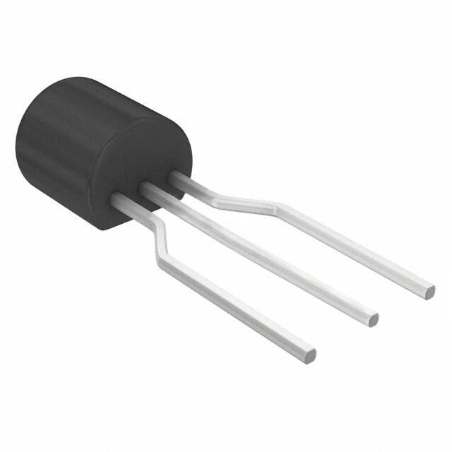


 工商网监
湘ICP备2023018690号
工商网监
湘ICP备2023018690号
