LMV331, NCV331, LMV393,
LMV339
Single, Dual, Quad General
Purpose, Low Voltage
Comparators
The LMV331 is a CMOS single channel, general purpose, low
voltage comparator. The LMV393 and LMV339 are dual and quad
channel versions, respectively. The LMV331/393/339 are specified
for 2.7 V to 5 V performance, have excellent input common−mode
range, low quiescent current, and are available in several space saving
packages.
The LMV331 is available in 5−pin SC−70 and TSOP−5 packages.
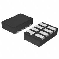
The LMV393 is available in a 8−pin Micro8t, SOIC−8, and a
UDFN8 package, and the LMV339 is available in a SOIC−14 and a
TSSOP−14 package.
The LMV331/393/339 are cost effective solutions for applications
where space saving, low voltage operation, and low power are the
primary specifications in circuit design for portable applications.
www.onsemi.com
5
1
1
1
Micro8
CASE 846A
Features
•
•
•
•
•
•
•
•
Guaranteed 2.7 V and 5 V Performance
Input Common−mode Voltage Range Extends to Ground
Open Drain Output for Wired−OR Applications
Low Quiescent Current: 60 mA/channel TYP @ 5 V
Low Saturation Voltage 200 mV TYP @ 5 V
Propagation Delay 200 ns TYP @ 5 V
NCV Prefix for Automotive and Other Applications Requiring
Unique Site and Control Change Requirements; AEC−Q100
Qualified and PPAP Capable
These Devices are Pb−Free, Halogen Free/BFR Free and are RoHS
Compliant
Battery Monitors
Notebooks and PDA’s
General Purpose Portable Devices
General Purpose Low Voltage Applications
8
8
1
1
SOIC−8
CASE 751
UDFN8
CASE 517AJ
1
1
SOIC−14
CASE 751A
Typical Applications
•
•
•
•
TSOP−5
CASE 483
SC−70
CASE 419A
TSSOP−14
CASE 948G
ORDERING INFORMATION
See detailed ordering and shipping information in the package
dimensions section on page 13 of this data sheet.
+VCC
R1
VIN
VCC
RPULL−UP
−
VO
VO
VT2
V+
RLOAD
+
VT1
0
VIN
Figure 2. Hysteresis Curve
R3
R2
Figure 1. Inverting
Comparator with Hysteresis
© Semiconductor Components Industries, LLC, 2014
June, 2017 − Rev. 8
1
Publication Order Number:
LMV331/D
�LMV331, NCV331, LMV393, LMV339
MARKING DIAGRAMS
SC−70
CASE 419A
TSOP−5
CASE 483
UDFN8
CASE 517AJ
5
3CAAYWG
G
CCAMG
G
CAMG
G
1
CA = Specific Device Code
A
= Assembly Location
M = Date Code
Y
= Year
G
= Pb−Free Package
W = Work Week
(Note: Microdot may be in either location)
G
= Pb−Free Package
(Note: Microdot may be in either location)
Micro8
SOIC−8
CASE 846A
CASE 751
8
8
CCA = Specific Device Code
M = Date Code
G
= Pb−Free Package
(Note: Microdot may be in either location)
V393
ALYW G
G
V393
AYWG
G
1
1
A
= Assembly Location
Y
= Year
W
= Work Week
G
= Pb−Free Package
(Note: Microdot may be in either location)
A
L
Y
W
G
= Assembly Location
= Wafer Lot
= Year
= Work Week
= Pb−Free Package
SOIC−14
CASE 751A
TSSOP−14
CASE 948G
14
14
LMV
339
ALYWG
G
LMV339
AWLYWWG
1
1
A
WL
Y
WW
G
A
L
Y
W
G
= Assembly Location
= Wafer Lot
= Year
= Work Week
= Pb−Free Package
= Assembly Location
= Wafer Lot
= Year
= Work Week
= Pb−Free Package
(Note: Microdot may be in either location)
PACKAGE PINOUTS
SC−70/TSOP−5
+IN
1
GND
2
−IN
Micro8 / SOIC−8 / UDFN8
5
VCC
Output A
+
−
3
4
OUTPUT
Inputs A
GND
1
8
2
7
3
4
−
+
−
+
SOIC−14 / TSSOP−14
VCC
Output 2
1
14
Output 3
Output B
Output 1
2
13
Output 4
VCC
3
12
GND
− Input 1
4
11
+ Input 4
10
− Input 4
9
+ Input 3
8
− Input 3
6
5
Inputs B
(Top Views)
(Top Views)
+ Input 1
5
− Input 2
6
+ Input 2
7
*
1
)
4
*2
)
3
(Top Views)
www.onsemi.com
2
)
*
)
*
�LMV331, NCV331, LMV393, LMV339
MAXIMUM RATINGS
Symbol
VS
Rating
Voltage on any Pin (referred to V− pin)
Value
Unit
5.5
V
VIDR
Input Differential Voltage Range
±Supply Voltage
V
TJ
Maximum Junction Temperature
150
°C
TA
Operating Ambient Temperature Range
°C
LMV331, LMV393, LMV339
NCV331 (Note 3)
−65 to 150
°C
Mounting Temperature (Infrared or Convection (1/16″ From Case for 30 Seconds))
260
°C
ESD Tolerance (Note 1)
Machine Model
Human Body Model
100
1000
Tstg
Storage Temperature Range
TL
VESD
−40 to 85
−40 to 125
V
Stresses exceeding those listed in the Maximum Ratings table may damage the device. If any of these limits are exceeded, device functionality
should not be assumed, damage may occur and reliability may be affected.
RECOMMENDED OPERATING CONDITIONS
Symbol
Parameter
VCC
Supply Voltage Temperature Range (Note 2)
qJA
Thermal Resistance
SC−70
TSOP−5
Micro8
SOIC−8
UDFN8
SOIC−14
TSSOP−14
Value
Unit
2.7 to 5.0
V
°C/W
280
333
238
212
350
156
190
1. Human Body Model, applicable std. MIL−STD−883, Method 3015.7. Machine Model, applicable std. JESD22−A115−A (ESD MM std. of
JEDEC) Field−Induced Charge−Device Model, applicable std. JESD22−C101−C (ESD FICDM std. of JEDEC).
2. The maximum power dissipation is a function of TJ(MAX), qJA. The maximum allowable power dissipation at any ambient temperature is
PD = (TJ(MAX) − TA)/qJA. All numbers apply for packages soldered directly onto a PC board.
3. NCV prefix is qualified for automotive usage.
www.onsemi.com
3
�LMV331, NCV331, LMV393, LMV339
2.7 V DC ELECTRICAL CHARACTERISTICS (All limits are guaranteed for TA = 25°C, V+ = 2.7 V, V− = 0 V, VCM = 1.35 V unless
otherwise noted.)
Parameter
Symbol
Typ
Max
Unit
VIO
1.7
9
mV
TC VIO
5
mV/°C
Input Bias Current (Note 4)
IB
很抱歉,暂时无法提供与“LMV393MUTAG”相匹配的价格&库存,您可以联系我们找货
免费人工找货