DATA SHEET
www.onsemi.com
Single and Dual Low
Voltage, Rail-to-Rail Input
and Output, Operational
Amplifiers
MARKING
DIAGRAMS
LMV931 (Single)
AAF MG
G
SC−70
CASE 419A
LMV931, LMV932
The LMV931 Single and LMV932 Dual are CMOS low−voltage
operational amplifiers which can operate on single−sided power
supplies (1.8 V to 5.0 V) with rail−to−rail input and output swing.
Both devices come in small state−of−the−art packages and require
very low quiescent current making them ideal for battery−operated,
portable applications such as notebook computers and hand−held
instruments. Rail−to−Rail operation provides improved signal−to−noise
performance plus the small packages allow for closer placement to
signal sources thereby reducing noise pickup.
The single LMV931 is offered in space saving SC70−5 package.
The dual LMV932 is in either a Micro8 or SOIC package. These small
packages are very beneficial for crowded PCB’s.
5
5
ADFAYWG
G
1
TSOP−5
CASE 483
1
M = Date Code
A
= Assembly Location
Y
= Year
W = Work Week
G
= Pb−Free Package
(Note: Microdot may be in either location)
LMV932 (Dual)
Features
8
• Performance Specified on Single−Sided Power Supply: 1.8 V, 2.7 V, and
•
•
•
•
•
•
5V
Small Packages:
LMV931 in a SC−70
LMV932 in a Micro8 or SOIC−8
No Output Crossover Distortion
Extended Industrial Temperature Range: −40°C to +125°C
Low Quiescent Current 210 mA, Max Per Channel
No Output Phase−Reversal from Overdriven Input
These are Pb−Free Devices
Micro8
CASE 846A
8
1
SOIC−8
CASE 751
• Notebook Computers, Portable Battery−Operated Instruments, PDA’s
• Active Filters, Low−Side Current Monitoring
RL = 600 W
TA = 25°C
0.09
1
LMV932
ALYW
G
A
= Assembly Location
Y
= Year
L
= Wafer Lot
W
= Work Week
G
= Pb−Free Package
(Note: Microdot may be in either location)
ORDERING INFORMATION
0.08
DV FROM RAIL (V)
1
8
Typical Applications
0.1
V932
AYWG
G
See detailed ordering and shipping information in the package
dimensions section on page 14 of this data sheet.
0.07
0.06
0.05
0.04
VOH
0.03
0.02
VOL
0.01
0 1.8
2.2
2.6
3
3.4
3.8
4.2
4.6
5
SUPPLY VOLTAGE (V)
Figure 1. Output Voltage Swing vs. Supply Voltage
© Semiconductor Components Industries, LLC, 2014
October, 2021 − Rev. 10
1
Publication Order Number:
LMV931/D
�LMV931, LMV932
PIN CONNECTIONS
SC70−5/TSOP−5
1
Micro8/SOIC−8
5
OUT A
1
IN A−
2
IN A+
3
VEE
4
VCC
+IN
2
+
−
VEE
3
4
−IN
OUTPUT
(Top View)
8 VCC
A
− +
7 OUT B
B
+ −
6 IN B−
5 IN B+
(Top View)
MAXIMUM RATINGS
Symbol
VS
Rating
Supply Voltage (Operating Range VS = 1.8 V to 5.5 V)
VIDR
Input Differential Voltage
VICR
Input Common Mode Voltage Range
Maximum Input Current
Value
Unit
5.5
V
$Supply Voltage
V
−0.5 to (VCC) + 0.5
V
10
mA
tSo
Output Short Circuit (Note 1)
Continuous
TJ
Maximum Junction Temperature (Operating Range −40°C to 85°C)
150
°C
qJA
Thermal Resistance:
280
333
238
°C/W
Tstg
Storage Temperature
−65 to 150
°C
260
°C
SC−70
TSOP−5
Micro8
Mounting Temperature (Infrared or Convection v 30 sec)
Stresses exceeding those listed in the Maximum Ratings table may damage the device. If any of these limits are exceeded, device functionality should not be assumed, damage may occur and reliability may be affected.
ESD data available upon request.
1. Continuous short−circuit operation to ground at elevated ambient temperature can result in exceeding the maximum allowed junction
temperature of 150°C. Output currents in excess of 45 mA over long term may adversely affect reliability. Shorting output to either VCC
or VEE will adversely affect reliability.
www.onsemi.com
2
�LMV931, LMV932
1.8 V DC ELECTRICAL CHARACTERISTICS (Note 2) Unless otherwise noted, all min/max limits are guaranteed for TA = 25°C,
VS = 1.8 V, VCM = VS/2, VO = VS/2 and RL > 1 MW. Typical specifications represent the most likely parametric norm.
Parameter
Input Offset Voltage
Input Offset Voltage
Average Drift
Symbol
Condition
VIO
Min
Typ
Max
Unit
LMV931 (Single) (−40°C to +125°C)
1
6
mV
LMV932 (Dual) (−40°C to +125°C)
1
7.5
TCVIO
5.5
mV/°C
Input Bias Current
IB
−40°C to +125°C
1 MW. Typical specifications represent the most likely parametric norm.
Parameter
Input Offset Voltage
Input Offset Voltage
Average Drift
Symbol
Condition
VIO
Min
Typ
Max
Unit
LMV931 (Single) (−40°C to +125°C)
1
6
mV
LMV932 (Dual) (−40°C to +125°C)
1
7.5
TCVIO
5.5
mV/°C
Input Bias Current
IB
−40°C to +125°C
很抱歉,暂时无法提供与“LMV931SN3T1G”相匹配的价格&库存,您可以联系我们找货
免费人工找货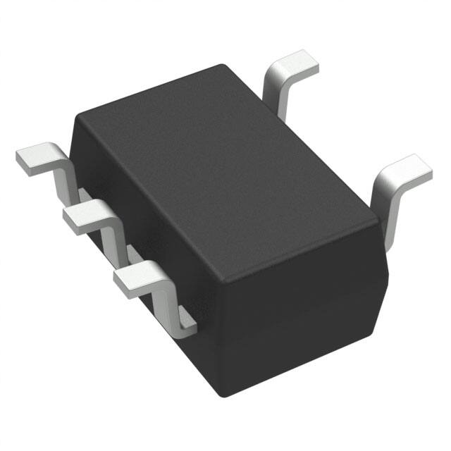


 工商网监
湘ICP备2023018690号
工商网监
湘ICP备2023018690号
