Linear LED Driver,
24-Channel, Bus Controlled
LV52511MNZ
Overview
The LV52511MN is a serial bus controlled linear low side driver for
LEDs (or other loads). The 24 channels are grouped in 3 color blocks
(RGB) of 8 channels each. The ON-time for each channel can be
programmed by an 8bit register. The reference current is programmed
by a single resistor, a 5bit register defines the current for each color
block as a fraction (3 to 100%) of the reference current to adjust for
color temperature.
Systems parameters can be programmed via 2 wire serial bus, or 3
wire SPI bus with EN, and I2C serial bus format (Hs-mode).
www.onsemi.com
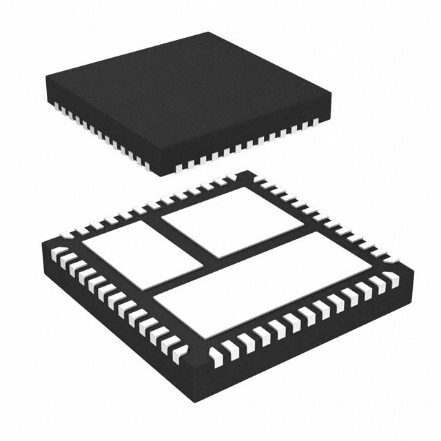
1 48
QFN48 7x7
CASE 485EB
Features
•
•
•
•
•
•
•
•
•
LED Supply from 3 V to 41 V with Transient Tolerance up to 42 V
System Supply from 3 V to 20 V with Transient Tolerance up to 24 V
Up to 60 mA Resistor Defined Maximum Current for All Channels
5 bit Individually Adjustable Current for each Color Group RGB
8 bit Luminance Dimming for each Channel
2 or 3 Wire Bus Interface with up to 56 Slave Addresses
Thermal and Undervoltage Lock-out Protection
Thermally Efficient Exposed Die 48 pin QFN Package for Operation
up to 85°C Ambient
These Devices are Pb-Free, Halogen Free/BFR Free and are RoHS
Compliant
Typical Applications
• Gaming (Slot Machine) and Entertainment Equipment
• LED Displays
• Digital Information Signs
MARKING DIAGRAM
1
XXXXXXX
ASWLYYWW
XXX
AS
WL
YY
WW
= Specific Device Code
= Assembly Location Code
= Wafer Lot Code
= Year
= Work Week
ORDERING INFORMATION
Device
Package
Shipping†
LV52511MNZTXG
QFN48
(Pb-Free/
Halogen Free)
2,500 /
Tape & Reel
†For information on tape and reel specifications,
including part orientation and tape sizes, please
refer to our Tape and Reel Packaging Specification
Brochure, BRD8011/D.
© Semiconductor Components Industries, LLC, 2016
October, 2019 − Rev. 1
1
Publication Order Number:
LV52511MNZ/D
�LV52511MNZ
12 V
LV52511MNZ Application (SVCC = 12 V)
1 mF
37
38
39
40
41
42
43
44
45
SVCC
46
27 kW
47
48
0.1 mF
36
35
VREF
24
25
23
26
12
22
27
11
21
28
TEST1
20
29
GND
19
30
Iref_R
18
31
Iref_G
17
32
Iref_B
16
33
RESET
15
OUTSCT
14
LVCC
13
CTLSCT
Figure 1. Typical Application Diagram
SDATA
SDEN
SDO
LEDB8
LEDG8
LEDR8
PGND3
LEDB7
LEDG7
LEDR7
48
47
46
45
44
43
42
41
40
39
38
LEDB6
SCLK
PINOUT
37
36
4
33
LEDB5
RESET
5
32
LEDG5
Iref−B
6
31
LEDR5
Iref−G
7
30
PGND2
8
29
LEDB4
SGND
9
28
LEDG4
TEST1
10
27
LEDR4
A0
11
26
LEDB3
A1
12
13
LEDG3
Iref−R
A2
14
15
16
17
18
19
20
21
22
23
25
24
LEDR3
OUTSCT
LEDB2
LVCC
LEDG2
34
LEDR2
3
PGND1
CTLSCT
LEDB1
LEDR6
LEDG1
35
LEDR1
2
A5
VREF
A4
1
A3
SVCC
Figure 2. Pin Assignment
www.onsemi.com
2
LEDG 6
�LV52511MNZ
PIN DESCRIPTIONS
Pin No.
Pin Name
I/O
Description
1
SVCC
−
System power supply input. For LED supply voltages from 3 to 20 V connect directly to LED supply. For higher LED voltages SVCC must be limited to 24 V (max)
2
VREF
O
Internal supply output pin. Regulates to 5 V if SVCC is higher than 5 V. Bypass with
a 0.1 mF capacitor
3
CTLSCT
I
Select pin for 2-wire or 3-wire interface and I2C. Tie to GND for 3-wire, tie to VREF
for 2wire bus, open for I2C bus
TYPE 1
4
OUTSCT
I
Analog three level selection pin to set current characteristics for the output channels. See “OUTSCT Setting” on page 10 for details
TYPE 1
5
RESET
I
Active high reset input pin. Clears all register settings.
Power on reset connect with VREF.
TYPE 2
6
Iref_B
O
Maximum reference current programming pin. Connect a resistor > 10 kW from this
pin to GND to define maximum LED current according to the following formula:
IREF = 1.2 × 580 / RT
TYPE 3
7
Iref_G
O
Maximum reference current programming pin. Connect a resistor > 10 kW from this
pin to GND to define maximum LED current according to the following formula:
IREF = 1.2 × 580 / RT
TYPE 3
8
Iref_R
O
Maximum reference current programming pin. Connect a resistor > 10 kW from this
pin to GND to define maximum LED current according to the following formula:
IREF = 1.2 × 580 / RT
TYPE 3
9
SGND
−
Analog circuit GND pin
10
TEST1
I
Test1 pin (connected to GND)
TYPE 4
11−16
A0−A5
I
Slave address setting pin. Refer to “Slave Address Setting” on page 11 for details
TYPE 5
17
LEDR1
O
LED red 1 current output pin
TYPE 6
18
LEDG1
O
LED green 1 current output pin
TYPE 6
19
LEDB1
O
LED blue 1 current output pin
TYPE 6
20
PGND1
−
GND pin dedicated for LED driver. Connect directly to ground plane
21
LEDR2
O
LED red 2 current output pin
TYPE 6
22
LEDG2
O
LED green 2 current output pin
TYPE 6
23
LEDB2
O
LED blue 2 current output pin
TYPE 6
24
LEDR3
O
LED red 3 current output pin
TYPE 6
25
LEDG3
O
LED green 3 current output pin
TYPE 6
26
LEDB3
O
LED blue 3 current output pin
TYPE 6
27
LEDR4
O
LED red 4 current output pin
TYPE 6
28
LEDG4
O
LED green 4 current output pin
TYPE 6
29
LEDB4
O
LED blue 4 current output pin
TYPE 6
30
PGND2
−
GND pin dedicated for LED driver. Connect directly to ground plane
31
LEDR5
O
LED red 5 current output pin
TYPE 6
32
LEDG5
O
LED green 5 current output pin
TYPE 6
33
LEDB5
O
LED blue 5 current output pin
TYPE 6
34
LVCC
−
Protection for LED drivers.
For higher LED voltages. LVCC must be limited to 42.0 V (max)
35
LEDR6
O
LED red 6 current output pin
TYPE 6
36
LEDG6
O
LED green 6 current output pin
TYPE 6
www.onsemi.com
3
Pin Circuit
�LV52511MNZ
PIN DESCRIPTIONS (continued)
Pin No.
Pin Name
I/O
Description
37
LEDB6
O
LED blue 6 current output pin
TYPE 6
38
LEDR7
O
LED red 7 current output pin
TYPE 6
39
LEDG7
O
LED green 7 current output pin
TYPE 6
40
LEDB7
O
LED blue 7 current output pin
TYPE 6
41
PGND3
−
GND pin dedicated for LED driver. Connect directly to ground plane
42
LEDR8
O
LED red 8 current output pin
TYPE 6
43
LEDG8
O
LED green 8 current output pin
TYPE 6
44
LEDB8
O
LED blue 8 current output pin
TYPE 6
45
SDO
O
Serial interface output pin.
TYPE 7
46
SDEN
I
Active high, 3-wire SPI Mode enable signal.
Must go low after each SPI frame. Not used for 2 wire interface
TYPE 8
47
SDATA
I/O
Serial interface data input / output pin.
Data frame consists of:
Slave_Address[7:0] – Register_Address[7:0] – Data1[7:0] … DataN[7:0]
TYPE 9
48
SCLK
I
Serial interface clock signal input pin.
Data is latched at the rising clock edge
TYPE 10
Exposed PAD
Pin Circuit
Connected to ground plane
PIN CIRCUIT
TYPE 2
TYPE 1
TYPE 3
VREF
VREF
VREF
1 MW
OUTSCT
CTLSCT
100 kW
12.5 kW
10 kW
10 kW
RESET
12.5 kW
IREF_B
IREF_G
IREF_R
100 pF
500 W
500 W
1.2 MW
BGR = 1.2 V
TYPE 4
TYPE 5
TYPE 6
VREF
TEST1
10 kW
LVCC
A0
A1
A2
A3
A4
A5
60 kW
TYPE 7
LEDO
10 kW
TYPE 8
VREF
1 kW
TYPE 9
SDATA
SDEN
SDO
1 kW
100 kW
ON: 2 wire
/3 wire
Acknowledge
TYPE 10
1 kW
SCLK
100 kW
ON: 2 wire
/3 wire
www.onsemi.com
4
�LV52511MNZ
SPECIFICATIONS
ABSOLUTE MAXIMUM RATINGS (Note 2)
Symbol
VCC max
Parameter
Conditions
Maximum Supply Voltage
Ratings
Unit
24
V
VLED
42
V
VREF
5.8
V
42
V
VO max
Output Voltage
LED off
IO max
Output Current
SVCC = 5.0 to 20 V
60/80
mA
IO max
Output Current
SVCC = 3.0 to 5 V
30/80
mA
Allowable Power Dissipation
TA ≤ 25_C (Note 1)
Pd max
Topr
Tj
Tstg
4.15
W
Operating Temperature
−25 to +85
°C
Operating Junction Temperature
−25 to +150
°C
Storage Temperature
−40 to +150
°C
Stresses exceeding those listed in the Maximum Ratings table may damage the device. If any of these limits are exceeded, device functionality
should not be assumed, damage may occur and reliability may be affected.
1. Specified board: 110 mm × 90 mm × 1.6 mm, glass epoxy board. Exposed Die-pad area is not a substrate mounting.
2. If you should intend to use this IC continuously under high temperature, high current, high voltage, or drastic temperature change, even if
it is used within the range of absolute maximum ratings or operating conditions, there is a possibility of decrease reliability. Please contact
us for a confirmation.
RECOMMENDED OPERATING CONDITIONS
Symbol
VCC op
Parameter
Operating Supply Voltage Range
Conditions
Ratings
Unit
SVCC
3.0 to 20
V
VLED op
LVCC
3.0 to 41
V
VREF op
VREF
3.0 to 5.5
V
Functional operation above the stresses listed in the Recommended Operating Ranges is not implied. Extended exposure to stresses beyond
the Recommended Operating Ranges limits may affect device reliability.
ELECTRICAL CHARACTERISTICS (TA = 25°C, 3.3 V < SVCC < 20 V)
Symbol
Parameter
Conditions
Min
Typ
Max
Unit
ICC1
Supply Current1
SVCC = 12 V/RESET = H LED OFF
1.2
1.9
2.6
mA
ICC2
Supply Current2
SVCC = 12 V/RESET = H
LED OFF SCLK = 5 MHz
1.8
3.0
4.2
mA
IMAX1R
LED Driver Output Current Rch
Iref-R = 27 kW, OUTSCT = L
24.25
25.80
27.35
mA
IMAX1G
LED Driver Output Current Gch
Iref-G = 27 kW, OUTSCT = L
24.25
25.80
27.35
mA
IMAX1B
LED Driver Output Current Bch
Iref-B = 27 kW, OUTSCT = L
24.25
25.80
27.35
mA
Line Regulation
VO = 0.7 to 4.0 V
(Same channel line regulation)
−5
−
−
%
Ron1
LED Output on Resistance 1
IO = 10 mA
−
10
20
W
Ileak
OFF Leak Current
LED OFF
−
−
1
mA
POR release voltage threshold
−
2.5
−
V
Undervoltage lockout threshold
−
2.3
−
V
4.8
5.1
5.4
V
DIL
VPOR
VCC Power on RESET Voltage
VRST
VREF1
VREF Voltage
SVCC = 12 V, IO = 30 mA
Product parametric performance is indicated in the Electrical Characteristics for the listed test conditions, unless otherwise noted. Product
performance may not be indicated by the Electrical Characteristics if operated under different conditions.
www.onsemi.com
5
�LV52511MNZ
CONTROL CIRCUIT (TA = 25°C, SVCC = 5.0 to 20 V)
Symbol
Parameter
VH1
H Level 1
VM1
Conditions
Min
Typ
Max
Unit
Input H level OUTSCT/CTLSCT
4.5
−
5.0
V
M Level 1
Input M level OUTSCT/CTLSCT
1.8
−
3.0
V
VL1
L Level 1
Input L level OUTSCT/CTLSCT
0
−
0.5
V
VH2
H Level 2
Input H level RESET
4.0
−
5.0
V
VL2
L Level 2
Input L level RESET
0
−
1.0
V
VH3
H Level 3
Input H level A0 to A5
3.5
−
5.0
V
VL3
L Level 3
Input L level A0 to A5
0
−
0.5
V
VH4
H Level 4
Input H level SCLK, SDATA, SDEN
4.0
−
5.0
V
VL4
L Level 4
Input L level SCLK, SDATA, SDEN
0
−
1.0
V
Min
Typ
Max
Unit
CONTROL CIRCUIT (TA = 25°C, SVCC = 3.3 V)
Symbol
Parameter
Conditions
VH1
H Level 1
Input H level OUTSCT/CTLSCT
2.8
−
3.3
V
VM1
M Level 1
Input M level OUTSCT/CTLSCT
1.2
−
1.8
V
VL1
L Level 1
Input L level OUTSCT/CTLSCT
0
−
0.5
V
VH2
H Level 2
Input H level RESET
2.7
−
3.3
V
VL2
L Level 2
Input L level RESETT
0
−
0.6
V
VH3
H Level 3
Input H level A0 to A5
2.7
−
3.3
V
VL3
L Level 3
Input L level A0 to A5
0
−
0.5
V
VH4
H Level 4
Input H level SCLK, SDATA, SDEN
2.7
−
3.3
V
VL4
L Level 4
Input L level SCLK, SDATA, SDEN
0
−
0.6
V
www.onsemi.com
6
�LV52511MNZ
SERIAL BUS TIMING CONDITIONS AT 2-WIRE SPI, AND 3-WIRE SPI
Min
Typ
Max
Unit
SDEN setup time relative to the rise of SCLK
90
−
−
ns
SDATA setup time relative to the rise of SCLK
60
−
−
ns
SDEN hold time relative to the fall of SCLK
200
−
−
ns
SDATA hold time relative to the fall of SCLK
60
−
−
ns
Low period pulse width of SCLK
90
−
−
ns
tw1H
High period pulse width of SCLK
90
−
−
ns
tw2L
Low period pulse width of SDEN
1
−
−
ms
Min
Typ
Max
Unit
0
−
1000
kHz
Symbol
ts0
Parameter
Data Setup Time
ts1
th0
Data Hold Time
th1
tw1L
Pulse Width
Conditions
SERIAL BUS TIMING CONDITIONS AT I2C FAST-MODE PLUS
Symbol
Parameter
Conditions
fsc1
SCL Clock Frequency
SCLK clock frequency
ts1
Data Setup Time
SCL setup time relative to the rise of SDA
0.26
−
−
ms
ts2
SDA setup time relative to the rise of SCL
50
−
−
ns
ts3
SCL setup time relative to the rise of SDA
0.26
−
−
ms
SCL hold time relative to the fall of SDA
−
−
−
ms
SDA hold time relative to the fall of SCL
0
−
−
ms
Low period pulse width of SCL
0.5
−
−
ms
High period pulse width of SCL
0.26
−
−
ms
Rise time of both SDA and SCL signals
−
−
120
ns
Fall time of both SDA and SCL signals
−
−
120
ns
0.5
−
−
ms
Min
Typ
Max
Unit
0
−
3.4
MHz
th1
Data Hold Time
th2
tw1L
Pulse Width
tw1H
ton
Input Signal
tof
tbuf
Bus Free Time
Bus free time between a STOP and START
condition
SERIAL BUS TIMING CONDITIONS AT I2C Hs-MODE
Symbol
Parameter
Conditions
fsc1
SCL Clock Frequency
SCLK clock frequency
ts1
Data Setup Time
SCL setup time relative to the rise of SDA
160
−
−
ns
ts2
SDA setup time relative to the rise of SCL
10
−
−
ns
ts3
SCL setup time relative to the rise of SDA
160
−
−
ns
SCL hold time relative to the fall of SDA
−
−
−
ns
SDA hold time relative to the fall of SCL
0
−
70
ns
Low period pulse width of SCL
160
−
−
ns
High period pulse width of SCL
60
−
−
ns
Rise time of SCL signals
10
−
40
ns
tcof
Fall time of SCL signals
10
−
40
ns
tdon
Rise time of SDA signals
10
−
80
ns
Tdof
Fall time of SDA signals
10
−
80
ns
th1
Data Hold Time
th2
tw1L
Pulse Width
tw1H
tcon
Input Signal
The ACK sink capability of the SDA pin is equal to FASTMODE. In case of requirement up to 20 mA, an external MOSFET
is needed.
www.onsemi.com
7
�LV52511MNZ
LEDB6
LEDR7
LEDG7
LEDB7
PGND3
LEDR8
LEDG8
LEDB8
SDO
SDEN
SDATA
SCLK
DETAILED FUNCTIONAL DESCRIPTION
Serial Bus
I/F
SVCC
LEDG6
LDO
BGR
VREF
LEDR6
CTLSCT
LVCC
OSC
POWER ON
RESET
RESET
Output Circuit
(Constant − current
/ Open − drain)
BRIGHTNESS
CONTROL
OUTSCT
LEDG5
PWM (8 bit)
Iref−B
Iref−G
LEDB5
I−REG D/A
Iref−R
Constant − current
BLED (5 bit)
LEDR5
Constant − current
GLED (5 bit)
PGND2
Constant − current
RLED (5 bit)
LEDB4
TSD
UVLO
SGND
LEDG4
TEST1
LEDR4
A0
LEDB3
ADDRESS
DECODER
A1
LEDG3
LEDR3
8
LEDB2
www.onsemi.com
LEDG2
LEDR2
PGND1
LEDB1
LEDG1
LEDR1
A5
A4
A3
A2
Figure 3. Block Diagram
�LV52511MNZ
System Startup and Shutdown (SVCC, RESET)
The LV52511MN is supplied via SVCC. If the voltage on
SVCC rises above the POR level of 2.5 V (typ) the system
RESET = H
setup registers are being reset to their default state, and the
reference internal reference circuit at VREF starts up.
SVCC
VREF Output = 5.1 V
Power ON Reset Voltage = 2.5 V
SVCC
Register data maintain
Power ON Reset
Reset Voltage = 2.3 V
Detect the UVLO voltage,
and internal reset is carried out
− Register data
3 msec
− LED output current
0V
When cancel the reset of the device, it is
necessary to remove power−on reset after
assuming it SVCC = 0 V
LVCC
Serial input
(SCLK, SDATA, SDEN)
3 msec
Not decided
SVCC
RESET
LVCC
3 msec
Serial input
(SCLK, SDATA, SDEN)
Not decided
Figure 4. SVCC Startup and Shutdown
Internal References (SVCC, VREF, Iref-R/G/B)
SVCC can be connected to the LED supply of the
application as long as that supply is between 3 and 20 V. If
the LED supply is higher than 20 V, SVCC must be supplied
from a separate source.
If SVCC drops below the undervoltage lockout level of
2.3 V (typ) the system shuts down.
An internal voltage reference of 5 V (typ) is generated at
VREF from SVCC. Do not connect external loads.
An LED reference current is defined by connecting
a resistor RRT between Iref-R/G/B and GND according to
the formula: IMAX = 1.2 × 580 / RRT. A fraction of this
current (3%−100%) is applied to each LED channel.
Table 1. INTERNAL REFERENCES
Iref-R/G/B Setting
Serial Setting Pin
Iref-R: resistance
Iref-G: VREF
Iref-B: VREF
The variable adjustment of the RGB electric current level by the register is possible by connecting
resistance to decide a current value to only Iref-R.
(for 00h for 01h 02h)
Iref-G,Iref-B connects with VREF terminal.
Iref-R: resistance
Iref-G: resistance
Iref-B: resistance
The current value of RGB is fixed by connecting resistance to decide a current value to RGB unit.
The adjustment of the register is not possible (it becomes fixed in max)
www.onsemi.com
9
�LV52511MNZ
LED Driver Configuration
(LEDR1−8, LEDG1−8, LEDB1−8, OUTSCT)
a percentage of the LED reference current IMAX.
Percentages of 3 to 100 of are possible.
The LEDs are connected between the system LED supply
and IC channels LED_R1−R8, LED_G1−G8, LED_B1−B8
such that the LED current flows into the IC. Depending on
the LED drive voltage, it is possible to connect a single LED
or a chain of LEDs.
The LV52511MN can adjust color temperature and
brightness for up to 24 LEDs. Color temperature is adjusted
by varying the LED current, and brightness (luminance) is
adjusted by varying the on-time of the LED a fixed time
period (duty-cycle).
Luminance Control
The brightness of each LED channel is defined by the duty
cycle Duty(%): the time tON the channel is active during a
time window tCYCLE. The duty cycle is defined by the
following formula. Duty(%) = 100 × tON / tCYCLE. Each
LED channel has an 8-bit register to vary the duty cycle
between OFF (0.0%) and 99.6% in steps of 0.39% each.
OUTSCT Settings
In addition to the settings mentioned above, it is also
possible to subdivide the 8 LED channels within the color
groups into 6 and 2 LED channels grouped in the following
way:
Color Temperature Control
The 24 LED channels are organized into 3 color groups
(Red, Green, Blue) of 8 channels each. The currents for each
color group are programmed by a 5 bit register as
Table 2. OUTSCT SETTINGS
LED Driver Output Pin
LEDR1−R6, LEDG1−G6, LEDB1−B6
OUTSCT Level
LEDR7/R8, LEDG7/G8, LEDB7/B8
L = −0.2 to 0.3 V
Constant current output
Set maximum current by built-in D/A (5 bits)
0.81 mA to 25.8 mA, RT1 = 27 kW
Same as the other LEDs
H = 4.7 to 5.0 V
Open drain output
Set current by external resistor
RON = 10 W
Same as the other LEDs
M = 1.8 to 3.0 V
Constant current output
Set maximum current by built-in D/A (5 bits)
0.81 mA to 25.8 mA, RT1 = 27 kW
Open drain output
Set current by external resistor
RON = 10 W
Thermal Considerations
Pdmax − Ta
5.0
Supplying a large number of LEDs from the LV52511MN
leads to a rise in chip temperature. The self-heating depends
on:
• the drive current IO flowing into the LED channel
• the voltage at the output VOUT of the LED channel
• and the duty cycle D they are driven with leading to the
following formula for dissipated power in each
channel:
P CH + I O
V OUT
D
4.15
Pdmax (W)
4.0
3.0
2.15
2.0
(eq. 1)
The only architecture sensitive value is VOUT. It must be
greater than 0.7 V (min) to allow for regulation, but also as
small as possible. It is therefore advisable to connect the
maximum possible number of LEDs in series to one channel.
The total power dissipation PTOT of the IC is then the sum
of all PCH together. PTOT must not exceed the power allowed
by the safe operating are shown in Figure 5.
1.0
0.0
−25
0
25
50
Ta (5C)
75
Figure 5. Safe Operating Area
www.onsemi.com
10
100
�LV52511MNZ
Serial Bus Communication
(SCLK, SDATA, SDEN, CTLSCT)
All parameters described above are written to the
LV52511MN via a single directional 2-wire or 3-wire serial
bus with a clock frequency of up to 5 MHz. The bus type is
defined by the state of pin CTLSCT (VREF = 2-wire,
GND = 3-wire). Furthermore, the setting of CTLSCT = M
supports I2C. It supports Hs-mode (3.4 MHz).
Each bus message consists of an 8bit slave (IC) address,
followed by an 8bit register address, followed by one or
more 8bit data words. The register address will
self-increment for consecutive data words as long as the
communication is valid. After the last address was written,
the next data word will be written to address 00h again. For
detailed information on addresses and register contents see
section”
Table 3. SERIAL SETTING PIN
CTLSCT Level
Figure 6. Board
Over Temperature Shutoff
To protect the circuit from permanent damage or fire,
overtemperature shutoff is implemented. If the junction
temperature of the IC reaches 175°C, all LED outputs are
turned OFF. The thermal shut down is not latched, s0 when
the temperature falls below 130°C activity resumes.
Serial Setting Pin
L = −0.2 to 0.3 V
3wire SPI serial bus
(SCLK, SDATA, SDEN) 5 MHz
H = 4.7 to 5.0 V
2wire SPI serial bus
(SCLK, SDATA) 5 MHz
M = 1.8 to 3.0 V
I2C serial bus
(SCLK, SDATA) Hs-mode
Slave Address (A5−A0)
Each IC is identified by its unique slave address. The most
significant two bits of the 8bit slave (IC) address are fixed
to 10b. 56 Slave addresses are hardware defined by pins
A0−A5 as described below.
Table 4. SLAVE ADDRESS (A5−A0)
ADDRESS
SA7
SA6
SA5
SA4
SA3
SA2
SA1
SA0
1
A5
A4
A3
A2
A1
A0
0
Terminal PIN (Input)
SLAVE ADDRESS
A5
A4
A3
A2
A1
A0
SA7
SA6
SA5
SA4
SA3
SA2
SA1
SA0
L
L
L
L
L
L
1
0
0
0
0
0
0
0
1
A5
A4
A3
A2
A1
A0
0
H
H
L
H
H
H
1
1
1
0
1
1
1
0
…
At the time of CTLSCT = L, H, the SLAVE setting is possible to 56.
At the time of CTLSCT = M, the SLAVE setting is possible to 48.
www.onsemi.com
11
�LV52511MNZ
3-wire Serial Bus Communication
(SCLK, SDATA, and SDEN)
In 3-wire communication a frame is started with a rising
edge of SDEN and terminated with a falling edge of SDEN.
SCLK latches data at the rising edge. The smallest data word
is 24bits long consisting of:
If the number of SCLK transitions is less than 23, Data is
not latched. If it is 25 or more, the register address is
automatically incremented and the next data word will be
latched after eight clock cycles.
Slave Address (8 bit) + Register Address (8 bit) + Data (8 bit)
SDEN
ts0
tw1H
th0
tw2L
SCLK
ts1
th1
tcy1
tw1L
SA7 SA6 SA5 SA4 SA3 SA2 SA1 SA0 A7
A6
A5
A4
A3
A2
A1
A0
D7
D6
D5
D4
D3
D2
D1
D0
SA7
Figure 7. 3-wire Serial Data Frame
Single Byte Programming into Address 02 h
Three Byte Programming into Address 02 h, 03 h and 04 h
SDEN
SDEN
SDATA
1 0 0 0 0 0 1 0 0 0 0 0 0 0 1 0
Slave address
Register address 02 h
is set
Data 1 (1 byte)
Data is written into
address 02 h
SDATA
1 0 0 0 0 0 1 0 0 0 0 0 0 0 1 0
Register address 02 h
Slave address
is set
SDEN
SDATA
Incomplete Data Size
SDEN
1 0 0 0 0 0 1 0 0 0 0 0 0 0 1 0
Register address 02 h
Slave address
is set
SDATA
Data 1 (1 byte)
Data is written into
address 02 h
1 0 0 0 1 0 0 0
Slave address
SDEN
SDATA
Data 2 (1 byte)
Data is written into
address 03 h
Data 3 (1 byte)
Data is written into
address 04 h
Data 3 (1 byte)
Data is written into
address 04 h
Slave Address Mismatch
SDEN
SDATA
Data 2 (1 byte)
Data is written into
address 03 h
− − − − − −
Ignore if data is less
than 1 byte
Figure 8. Data Write Examples into Slave 82h
www.onsemi.com
12
Data 1 (1 byte)
Data is written into
address 02 h
�LV52511MNZ
after eight address bits. The third byte is the data byte which
was addressed by the register address received before. The
data byte will be latched after receiving a BLANK “0” in
position nine after eight data bits.
When data bytes continue after this, the register address
will be automatically incremented after each byte transfer is
completed after receiving BLANK “0”.
If the BLANK after a data transfer is “1”, including slave
address and register address, the single byte data just before
it will not be written, and subsequent data is ignored until
another START condition is detected.
2-wire Serial Bus Communication (SCLK, SDATA)
In 2-wire communication the LV52511MN watches
SDATA at every rising SCLK edge. A data frame begins
after START condition: nine consecutive detections of a “1”
(high) followed by a “0” (BLANK). This is true even during
an ongoing data transfer: serial communication will
restarted by a START condition (“111111111”) + BLANK
(“0”).
After start detection, the eight bit slave address will be
latched after receiving a BLANK (0h) with the ninth bit. The
register address will be latched after receiving a BLANK “0”
bit
SDATA
Parameter
ST8 ST7 ST6 ST5 ST4 ST3 ST2 ST1 ST0 BL SA7 SA6 SA5 SA4 SA3 SA2 SA1 SA0 BL A7
1
1
1
1
1
1
Start Condition
1
1
1
0
BLANK
1
0
0
Slave Address
A6
A5
A4
A3
A2
A1
A0
BL
D7
D6
D5
D4
D3 D2
D1
D0
BL
0
0
0
BLANK
BLANK
BLANK
Register Address
Fix Slave Address
Fix Register Address
Data
Fix Data
Figure 9. 2-wire Serial Communication Frame
Minimum Data length is 37 bits:
Start condition “111111111” (9bit) + BLANK (“0”) +
Slave address (8bit) + BLANK (“0”) +
Register address (8bit) + BLANK (“0”) +
Data (8bit) + BLANK (“0”).
NOTE: When SCLK is less than 27th clocks and/or
BLANK is “1” instead of “0” after start
detection, will not take in SDATA. When SCLK
is higher than 28th clock track, start detection is
confirmed, register address is incremented every
1 byte (8bit) + BLANK (“0”).
www.onsemi.com
13
�LV52511MNZ
SDATA
1
1
1
1
1
1
1
1
1
1
1
1
0
Start condition
Start an action to take in new serial data after this
BL
Start detection
Communication Begins with a BLANK “0” after 9 (or more) ones (“1”)
SDATA
1
1
1
1
1
1
1
1
1
0
1
0
0
BL
Start condition
0
0
0
1
0
Start detection
0
0
BL
Slave address
0
0
0
0
0
1
0
DATA1 (1 byte)
0
Register address is written in
Slave address is written in
0
BL Data is transferred for address 02 h BL
Register address 02 h is set
DATA1 is written in
Single Byte Programming into Address 02 h
SDATA
1
1
1
1
1
1
1
1
1
0
1
0
0
BL
Start condition
0
0
0
Start detection
DATA2 (1 byte)
1
0
0
0
0
0
0
0
1
0
0
DATA1 (1 byte)
0
BL Data is transferred for address 02 h BL
Register address 02 h is set
Register address is written in
Slave address is written in
DATA3 (1 byte)
0
0
BL
Slave address
DATA1 is written in
0
Data is transferred for address 03 h BL Data is transferred for address 04 h BL
DATA2 is written in
DATA3 is written in
Three Byte Programming into Addresses 02 h, 03 h and 04 h without Termination
SDATA
1
1
1
1
1
1
1
1
1
0
Start condition
1
0
0
0
0
0
1
0
Slave address
BL
Start detection
0
0
0
0
0
0
0
1
0
0
DATA1 (1 byte)
Register address is written in
Slave address is written in
0
BL Data is transferred for address 02 h BL
Register address 02 h is set
BL
DATA1 is written in
1
DATA2 (1 byte)
Data is transferred for address 03 h BL
The subsequent data is ignored until “start condition”
DATA2 is written in
Frame Termination by Sending “1” as BLANK after Dual Data Transfer
SDATA
1
1
1
1
1
1
1
1
1
0
1
0
BL
Start condition
0
0
0
0
1
0
0
Start detection
0
BL
Slave address
0
0
0
0
0
1
Register address 02 h is set
0
1
BL
The subsequent data is ignored until “start condition”
Register address is written in
Slave address is written in
Frame Termination by Sending “1” as a Blank before Data Transfer
SDATA
1
1
1
1
1
1
Start condition
1
1
1
0
1
BL
0
0
0
0
0
Slave address
Start detection
1
0
0
BL
The subsequent data is ignored until “start condition”
Slave address is written in
Slave Address Mismatch
Figure 10. Data Write Examples into Slave 82h
www.onsemi.com
14
�LV52511MNZ
I 2C Serial Bus Communication (SCLK, SDATA)
In 2-wire communication, LV52511MN accepts the
format corresponding to the standard of I2C.
It is Fast-mode Plus and higher-speed communicating
Hs-mode.
twH
SCL
twL
th1
tbuf
th2
SDA
th1
ts1
th2
START Condition
ts3
Retransmission Start Condition
ton
STOP Condition
tof
Input signal condition
Figure 11.
As for start condition and the stop condition I2C bus, SCL
has that SDA is kept between “H” by the constant state like
the chart below during movement performing data
transmission basically.
In addition, SCL and SDA are in a condition of “H”
together when data transmission is not carried out. It
becomes, and, at the time of this SCL = SDA = H, access is
started by a start condition when I change SDA into L from
H.
When SCL changes SDA into “H” from “L” at the time of
H, it becomes a stop condition and becomes the end of the
access.
SCL
START Condition
th2
STOP Condition
SCL
SDA
ts 2
SDA
Figure 12.
th2
The READ mode does not support.
Figure 13.
www.onsemi.com
15
�LV52511MNZ
REGISTER MAP
After POR all registers are cleared.
Table 5. COLOR TEMPERATURE REGISTERS
Addr.
Register
00h
LEDR Current
01h
D[7]
D[6]
D[5]
D[4]
D[3]
0
0
0
0
0
0
0
0
0
0
0
0
0
0
0
0
0
0
0
0
D[2]
D[1]
D[0]
0
0
0
3% of Imax
(0.81 mA @ RT = 27 kW)
0
0
0
1
6% of Imax
(1.61 mA @ RT = 27 kW)
0
0
0
1
0
9% of Imax
(2.42 mA @ RT = 27 kW)
0
0
0
1
1
13% of Imax
(3.23 mA @ RT = 27 kW)
0
0
0
1
0
0
16% of Imax
(4.03 mA @ RT = 27 kW)
0
0
0
1
0
1
19% of Imax
(4.84 mA @ RT = 27 kW)
0
0
0
0
1
1
0
22% of Imax
(5.64 mA @ RT = 27 kW)
0
0
0
0
0
1
1
1
25% of Imax
(6.45 mA @ RT = 27 kW)
0
0
0
0
1
0
0
0
28% of Imax
(7.26 mA @ RT = 27 kW)
0
0
0
0
1
0
0
1
31% of Imax
(8.06 mA @ RT = 27 kW)
0
0
0
0
1
0
1
0
34% of Imax
(8.87 mA @ RT = 27 kW)
0
0
0
0
1
0
1
1
38% of Imax
(9.68 mA @ RT = 27 kW)
0
0
0
0
1
1
0
0
41% of Imax
(10.48 mA @ RT = 27 kW)
0
0
0
0
1
1
0
1
44% of Imax
(11.29 mA @ RT = 27 kW)
0
0
0
0
1
1
1
0
47% of Imax
(12.09 mA @ RT = 27 kW)
0
0
0
0
1
1
1
1
50% of Imax
(12.90 mA @ RT = 27 kW)
0
0
0
1
0
0
0
0
53% of Imax
(13.71 mA @ RT = 27 kW)
0
0
0
1
0
0
0
1
56% of Imax
(14.51 mA @ RT = 27 kW)
0
0
0
1
0
0
1
0
59% of Imax
(15.32 mA @ RT = 27 kW)
0
0
0
1
0
0
1
1
63% of Imax
(16.13 mA @ RT = 27 kW)
0
0
0
1
0
1
0
0
66% of Imax
(16.93 mA @ RT = 27 kW)
0
0
0
1
0
1
0
1
69% of Imax
(17.74 mA @ RT = 27 kW)
0
0
0
1
0
1
1
0
72% of Imax
(18.54 mA @ RT = 27 kW)
0
0
0
1
0
1
1
1
75% of Imax
(19.35 mA @ RT = 27 kW)
0
0
0
1
1
0
0
0
78% of Imax
(20.16 mA @ RT = 27 kW)
0
0
0
1
1
0
0
1
81% of Imax
(20.96 mA @ RT = 27 kW)
0
0
0
1
1
0
1
0
84% of Imax
(21.77 mA @ RT = 27 kW)
0
0
0
1
1
0
1
1
88% of Imax
(22.58 mA @ RT = 27 kW)
0
0
0
1
1
1
0
0
91% of Imax
(23.38 mA @ RT = 27 kW)
0
0
0
1
1
1
0
1
94% of Imax
(24.19 mA @ RT = 27 kW)
0
0
0
1
1
1
1
0
97% of Imax
(24.99 mA @ RT = 27 kW)
0
0
0
1
1
1
1
1
Imax
(25.80 mA @ RT = 27 kW)
0
0
0
0
0
0
0
0
3% of Imax
(0.81 mA @ RT = 27 kW)
0
0
0
0
0
0
0
1
6% of Imax
(1.61 mA @ RT = 27 kW)
0
0
0
0
0
0
1
0
9% of Imax
(2.42 mA @ RT = 27 kW)
0
0
0
0
0
0
1
1
13% of Imax
(3.23 mA @ RT = 27 kW)
0
0
0
0
0
1
0
0
16% of Imax
(4.03 mA @ RT = 27 kW)
0
0
0
0
0
1
0
1
19% of Imax
(4.84 mA @ RT = 27 kW)
0
0
0
0
0
1
1
0
22% of Imax
(5.64 mA @ RT = 27 kW)
I_LEDR[4:0]
LEDG Current
LEDR Current Setting (LEDR1~LEDR8)
I_LEDG[4:0]
LEDG Current Setting (LEDG1~LEDG8)
www.onsemi.com
16
Description
�LV52511MNZ
Table 5. COLOR TEMPERATURE REGISTERS (continued)
Addr.
02h
Register
D[7]
D[6]
D[5]
D[4]
D[3]
D[2]
D[1]
D[0]
0
0
0
0
0
1
1
1
25% of Imax
(6.45 mA @ RT = 27 kW)
0
0
0
0
1
0
0
0
28% of Imax
(7.26 mA @ RT = 27 kW)
0
0
0
0
1
0
0
1
31% of Imax
(8.06 mA @ RT = 27 kW)
0
0
0
0
1
0
1
0
34% of Imax
(8.87 mA @ RT = 27 kW)
0
0
0
0
1
0
1
1
38% of Imax
(9.68 mA @ RT = 27 kW)
0
0
0
0
1
1
0
0
41% of Imax
(10.48 mA @ RT = 27 kW)
0
0
0
0
1
1
0
1
44% of Imax
(11.29 mA @ RT = 27 kW)
0
0
0
0
1
1
1
0
47% of Imax
(12.09 mA @ RT = 27 kW)
0
0
0
0
1
1
1
1
50% of Imax
(12.90 mA @ RT = 27 kW)
0
0
0
1
0
0
0
0
53% of Imax
(13.71 mA @ RT = 27 kW)
0
0
0
1
0
0
0
1
56% of Imax
(14.51 mA @ RT = 27 kW)
0
0
0
1
0
0
1
0
59% of Imax
(15.32 mA @ RT = 27 kW)
0
0
0
1
0
0
1
1
63% of Imax
(16.13 mA @ RT = 27 kW)
0
0
0
1
0
1
0
0
66% of Imax
(16.93 mA @ RT = 27 kW)
0
0
0
1
0
1
0
1
69% of Imax
(17.74 mA @ RT = 27 kW)
0
0
0
1
0
1
1
0
72% of Imax
(18.54 mA @ RT = 27 kW)
0
0
0
1
0
1
1
1
75% of Imax
(19.35 mA @ RT = 27 kW)
0
0
0
1
1
0
0
0
78% of Imax
(20.16 mA @ RT = 27 kW)
0
0
0
1
1
0
0
1
81% of Imax
(20.96 mA @ RT = 27 kW)
0
0
0
1
1
0
1
0
84% of Imax
(21.77 mA @ RT = 27 kW)
0
0
0
1
1
0
1
1
88% of Imax
(22.58 mA @ RT = 27 kW)
0
0
0
1
1
1
0
0
91% of Imax
(23.38 mA @ RT = 27 kW)
0
0
0
1
1
1
0
1
94% of Imax
(24.19 mA @ RT = 27 kW)
0
0
0
1
1
1
1
0
97% of Imax
(24.99 mA @ RT = 27 kW)
0
0
0
1
1
1
1
1
Imax
(25.80 mA @ RT = 27 kW)
0
0
0
0
0
0
0
0
3% of Imax
(0.81 mA @ RT = 27 kW)
0
0
0
0
0
0
0
1
6% of Imax
(1.61 mA @ RT = 27 kW)
0
0
0
0
0
0
1
0
9% of Imax
(2.42 mA @ RT = 27 kW)
0
0
0
0
0
0
1
1
13% of Imax
(3.23 mA @ RT = 27 kW)
0
0
0
0
0
1
0
0
16% of Imax
(4.03 mA @ RT = 27 kW)
0
0
0
0
0
1
0
1
19% of Imax
(4.84 mA @ RT = 27 kW)
0
0
0
0
0
1
1
0
22% of Imax
(5.64 mA @ RT = 27 kW)
0
0
0
0
0
1
1
1
25% of Imax
(6.45 mA @ RT = 27 kW)
0
0
0
0
1
0
0
0
28% of Imax
(7.26 mA @ RT = 27 kW)
0
0
0
0
1
0
0
1
31% of Imax
(8.06 mA @ RT = 27 kW)
0
0
0
0
1
0
1
0
34% of Imax
(8.87 mA @ RT = 27 kW)
0
0
0
0
1
0
1
1
38% of Imax
(9.68 mA @ RT = 27 kW)
0
0
0
0
1
1
0
0
41% of Imax
(10.48 mA @ RT = 27 kW)
0
0
0
0
1
1
0
1
44% of Imax
(11.29 mA @ RT = 27 kW)
0
0
0
0
1
1
1
0
47% of Imax
(12.09 mA @ RT = 27 kW)
0
0
0
0
1
1
1
1
50% of Imax
(12.90 mA @ RT = 27 kW)
0
0
0
1
0
0
0
0
53% of Imax
(13.71 mA @ RT = 27 kW)
0
0
0
1
0
0
0
1
56% of Imax
(14.51 mA @ RT = 27 kW)
0
0
0
1
0
0
1
0
59% of Imax
(15.32 mA @ RT = 27 kW)
LEDB Current
I_LEDB[4:0]
LEDB Current Setting (LEDB1~LEDB8)
www.onsemi.com
17
Description
�LV52511MNZ
Table 5. COLOR TEMPERATURE REGISTERS (continued)
Addr.
Register
D[7]
D[6]
D[5]
D[4]
D[3]
D[2]
D[1]
D[0]
Description
0
0
0
1
0
0
1
1
63% of Imax
(16.13 mA @ RT = 27 kW)
0
0
0
1
0
1
0
0
66% of Imax
(16.93 mA @ RT = 27 kW)
0
0
0
1
0
1
0
1
69% of Imax
(17.74 mA @ RT = 27 kW)
0
0
0
1
0
1
1
0
72% of Imax
(18.54 mA @ RT = 27 kW)
0
0
0
1
0
1
1
1
75% of Imax
(19.35 mA @ RT = 27 kW)
0
0
0
1
1
0
0
0
78% of Imax
(20.16 mA @ RT = 27 kW)
0
0
0
1
1
0
0
1
81% of Imax
(20.96 mA @ RT = 27 kW)
0
0
0
1
1
0
1
0
84% of Imax
(21.77 mA @ RT = 27 kW)
0
0
0
1
1
0
1
1
88% of Imax
(22.58 mA @ RT = 27 kW)
0
0
0
1
1
1
0
0
91% of Imax
(23.38 mA @ RT = 27 kW)
0
0
0
1
1
1
0
1
94% of Imax
(24.19 mA @ RT = 27 kW)
0
0
0
1
1
1
1
0
97% of Imax
(24.99 mA @ RT = 27 kW)
0
0
0
1
1
1
1
1
Imax
(25.80 mA @ RT = 27 kW)
Table 6. LUMINANCE REGISTERS
Addr.
Register
D[7]
D[6]
D[5]
D[4]
D[3]
D[2]
D[1]
D[0]
Description
03h
PWM SEL
LEDR
R8
R7
R6
R5
R4
R3
R2
R1
Select PWM or Full on for LEDR1~LEDR8
0
1
0
1
0
1
0
1
0
1
0
1
0
1
0
1
0: PWM mode
1: Full on (100% PWM)
PWM SEL
LEDG
G8
G7
G6
G5
G4
G3
G2
G1
Select PWM or Full on for LEDG1~LEDG8
0
1
0
1
0
1
0
1
0
1
0
1
0
1
0
1
0: PWM mode
1: Full on (100% PWM)
PWM SEL
LEDB
B8
B7
B6
B5
B4
B3
B2
B1
Select PWM or Full on for LEDB1~LEDB8
0
1
0
1
0
1
0
1
0
1
0
1
0
1
0
1
0: PWM mode
1: Full on (100% PWM)
LEDR1 Duty
R1[7]
R1[6]
R1[5]
R1[4]
R1[3]
R1[2]
R1[1]
R1[0]
PWM duty setting for LEDR1
0
0
0
0
0
0
0
0
04h
05h
06h
R1[7:0]
1
07h
LEDG1 Duty
1
1
1
Duty(%) = 0.0%
Duty(%) = R1[7:0] / 256
1
1
1
G1[7:0]
1
Duty(%) = 99.6%
Duty(%) = G1[7:0] / 256
08h
LEDB1 Duty
B1[7:0]
Duty(%) = B1[7:0] / 256
09h
LEDR2 Duty
R2[7:0]
Duty(%) = R2[7:0] / 256
0ah
LEDG2 Duty
G2[7:0]
Duty(%) = G2[7:0] / 256
0bh
LEDB2 Duty
B2[7:0]
Duty(%) = B2[7:0] / 256
0ch
LEDR3 Duty
R3[7:0]
Duty(%) = R3[7:0] / 256
0dh
LEDG3 Duty
G3[7:0]
Duty(%) = G3[7:0] / 256
0eh
LEDB3 Duty
B3[7:0]
Duty(%) = B3[7:0] / 256
0fh
LEDR4 Duty
R4[7:0]
Duty(%) = R4[7:0] / 256
10h
LEDG4 Duty
G4[7:0]
Duty(%) = G4[7:0] / 256
11h
LEDB4 Duty
B4[7:0]
Duty(%) = B4[7:0] / 256
12h
LEDR5 Duty
R5[7:0]
Duty(%) = R5[7:0] / 256
13h
LEDG5 Duty
G5[7:0]
Duty(%) = G5[7:0] / 256
14h
LEDB5 Duty
B5[7:0]
Duty(%) = B5[7:0] / 256
15h
LEDR6 Duty
R6[7:0]
Duty(%) = R6[7:0] / 256
16h
LEDG6 Duty
G6[7:0]
Duty(%) = G6[7:0] / 256
17h
LEDB6 Duty
B6[7:0]
Duty(%) = B6[7:0] / 256
www.onsemi.com
18
�LV52511MNZ
Table 6. LUMINANCE REGISTERS (continued)
Addr.
Register
D[7]
D[6]
D[5]
D[4]
D[3]
D[2]
D[1]
D[0]
Description
18h
LEDR7 Duty
R7[7:0]
Duty(%) = R7[7:0] / 256
19h
LEDG7 Duty
G7[7:0]
Duty(%) = G7[7:0] / 256
1ah
LEDB7 Duty
B7[7:0]
Duty(%) = B7[7:0] / 256
1bh
LEDR8 Duty
R8[7:0]
Duty(%) = R8[7:0] / 256
1ch
LEDG8 Duty
G8[7:0]
Duty(%) = G8[7:0] / 256
1dh
LEDB8 Duty
B8[7:0]
Duty(%) = B8[7:0] / 256
20h
Group1 Duty
R1/R2/R3/R4/R5/R6/R7/R8[7:0]
Duty(%) = Group1 [7:0] / 256
21h
Group2 Duty
G1/G2/G3/G4/G5/G6/G7/G8[7:0]
Duty(%) = Group2 [7:0] / 256
22h
Group3 Duty
B1/B2/B3/B4/B5/B6/B7/B8[7:0]
Duty(%) = Group3 [7:0] / 256
23h
Group4 Duty
R1/G1/B1/R2/G2/B2[7:0]
Duty(%) = Group4 [7:0] / 256
24h
Group5 Duty
R3/G3/B3/R4/G4/B4[7:0]
Duty(%) = Group5 [7:0] / 256
25h
Group6 Duty
R5/G5/B5/R6/G6/B6[7:0]
Duty(%) = Group6 [7:0] / 256
26h
Group7 Duty
R7/G7/B7/R8/G8/B8[7:0]
Duty(%) = Group7 [7:0] / 256
1eh
1fh
When you transmit data of the group setting. please be careful because data of the individual setting update it.
www.onsemi.com
19
�MECHANICAL CASE OUTLINE
PACKAGE DIMENSIONS
QFN48 7x7, 0.5P
CASE 485EB
ISSUE O
1 48
SCALE 2:1
PIN 1
LOCATION
ÈÈ
ÈÈ
ÈÈ
D
A B
L1
DETAIL A
DIM
A
A1
A3
b
D
D2
E
E2
e
L
L1
ALTERNATE TERMINAL
CONSTRUCTIONS
E
ÉÉ
ÉÉ
ÇÇ
EXPOSED Cu
0.10 C
0.10 C
L
L
2X
2X
DATE 07 JUL 2015
NOTES:
1. DIMENSIONS AND TOLERANCING PER ASME
Y14.5M, 1994.
2. CONTROLLING DIMENSION: MILLIMETERS.
3. DIMENSION b APPLIES TO THE PLATED
TERMINAL AND IS MEASURED ABETWEEN
0.15 AND 0.25 MM FROM THE TERMINAL TIP.
4. COPLANARITY APPLIES TO THE EXPOSED
PAD AS WELL AS THE TERMINALS.
TOP VIEW
MOLD CMPD
DETAIL B
DETAIL B
ALTERNATE
CONSTRUCTION
(A3)
0.10 C
GENERIC
MARKING DIAGRAM*
A
0.08 C
1
A1
NOTE 4
C
SIDE VIEW
SEATING
PLANE
XXXXXXXXX
XXXXXXXXX
AWLYYWWG
0.10 C A B
D2
DETAIL A
13
A
WL
YY
WW
G
25
12
0.10 C A B
E2
1
36
48
48X
L
MILLIMETERS
MIN
MAX
0.80
0.90
0.00
0.05
0.20 REF
0.20
0.30
7.00 BSC
5.20
5.40
7.00 BSC
5.20
5.40
0.50 BSC
0.35
0.45
0.00
0.15
37
e
e/2
BOTTOM VIEW
48X
b
0.10 C A B
0.05 C
NOTE 3
= Assembly Location
= Wafer Lot
= Year
= Work Week
= Pb−Free Package
*This information is generic. Please refer
to device data sheet for actual part
marking.
Pb−Free indicator, “G” or microdot “ G”,
may or may not be present.
RECOMMENDED
SOLDERING FOOTPRINT*
2X
5.52
48X
0.63
1
2X
7.30
PACKAGE
OUTLINE
48X
0.32
0.50 PITCH
DIMENSIONS: MILLIMETERS
*For additional information on our Pb−Free strategy and soldering
details, please download the ON Semiconductor Soldering and
Mounting Techniques Reference Manual, SOLDERRM/D.
DOCUMENT NUMBER:
DESCRIPTION:
98AON99699F
QFN48 7X7, 0.50P
Electronic versions are uncontrolled except when accessed directly from the Document Repository.
Printed versions are uncontrolled except when stamped “CONTROLLED COPY” in red.
PAGE 1 OF 1
ON Semiconductor and
are trademarks of Semiconductor Components Industries, LLC dba ON Semiconductor or its subsidiaries in the United States and/or other countries.
ON Semiconductor reserves the right to make changes without further notice to any products herein. ON Semiconductor makes no warranty, representation or guarantee regarding
the suitability of its products for any particular purpose, nor does ON Semiconductor assume any liability arising out of the application or use of any product or circuit, and specifically
disclaims any and all liability, including without limitation special, consequential or incidental damages. ON Semiconductor does not convey any license under its patent rights nor the
rights of others.
© Semiconductor Components Industries, LLC, 2019
www.onsemi.com
�onsemi,
, and other names, marks, and brands are registered and/or common law trademarks of Semiconductor Components Industries, LLC dba “onsemi” or its affiliates
and/or subsidiaries in the United States and/or other countries. onsemi owns the rights to a number of patents, trademarks, copyrights, trade secrets, and other intellectual property.
A listing of onsemi’s product/patent coverage may be accessed at www.onsemi.com/site/pdf/Patent−Marking.pdf. onsemi reserves the right to make changes at any time to any
products or information herein, without notice. The information herein is provided “as−is” and onsemi makes no warranty, representation or guarantee regarding the accuracy of the
information, product features, availability, functionality, or suitability of its products for any particular purpose, nor does onsemi assume any liability arising out of the application or use
of any product or circuit, and specifically disclaims any and all liability, including without limitation special, consequential or incidental damages. Buyer is responsible for its products
and applications using onsemi products, including compliance with all laws, regulations and safety requirements or standards, regardless of any support or applications information
provided by onsemi. “Typical” parameters which may be provided in onsemi data sheets and/or specifications can and do vary in different applications and actual performance may
vary over time. All operating parameters, including “Typicals” must be validated for each customer application by customer’s technical experts. onsemi does not convey any license
under any of its intellectual property rights nor the rights of others. onsemi products are not designed, intended, or authorized for use as a critical component in life support systems
or any FDA Class 3 medical devices or medical devices with a same or similar classification in a foreign jurisdiction or any devices intended for implantation in the human body. Should
Buyer purchase or use onsemi products for any such unintended or unauthorized application, Buyer shall indemnify and hold onsemi and its officers, employees, subsidiaries, affiliates,
and distributors harmless against all claims, costs, damages, and expenses, and reasonable attorney fees arising out of, directly or indirectly, any claim of personal injury or death
associated with such unintended or unauthorized use, even if such claim alleges that onsemi was negligent regarding the design or manufacture of the part. onsemi is an Equal
Opportunity/Affirmative Action Employer. This literature is subject to all applicable copyright laws and is not for resale in any manner.
PUBLICATION ORDERING INFORMATION
LITERATURE FULFILLMENT:
Email Requests to: orderlit@onsemi.com
onsemi Website: www.onsemi.com
◊
TECHNICAL SUPPORT
North American Technical Support:
Voice Mail: 1 800−282−9855 Toll Free USA/Canada
Phone: 011 421 33 790 2910
Europe, Middle East and Africa Technical Support:
Phone: 00421 33 790 2910
For additional information, please contact your local Sales Representative
�


 工商网监
湘ICP备2023018690号
工商网监
湘ICP备2023018690号
