BLDC Motor Pre-driver with
Speed Control, Single-phase,
12 V, 24 V and 48 V
LV8310H�
Overview
The LV8310HGR2G is a pre-driver for a 12 V, 24 V and 48 V single
phase BLDC motor, which controls motor rotational speed with the
built-in closed loop speed controller. Its target speed can be set by
input PWM duty cycle. The speed curve setting can be stored to the
internal nonvolatile memory (NVM). In addition, Lead-angle can also
be adjusted by the configuration saved in the internal NVM. Thus, it
can drive various kinds of motors at high efficiency and low noise.
www.onsemi.com
16
1
Features
TSSOP−16
CASE 948F
• Driver Output for External Power FETs
(P-MOS High Side, N-MOS Low Side)
• Selectable High Side Gate Driver Polarity: One for 12 V Motor
•
•
•
•
•
•
•
•
•
•
•
•
•
•
•
Voltage and the other for 24 V/48 V Motor Voltage with External
Level Shifter FET
PI Closed Loop Speed Control Function
Single-phase Full Wave Driver
PWM Duty Cycle Input (25 Hz to 100 kHz)
Soft Start-up Function
PWM Soft Switching Phase Transitions
Soft PWM Duty Cycle Transitions (Changing the Target Speed
Gradually)
Built-in Current Limit Function and Over Current Protection
Function
Built-in Thermal Protection Function
Built-in Locked Rotor Protection and Automatic Recovery Function
FG or RD Signal Output Selectable
Dynamic Lead Angle Adjustment with Respect to Input Duty Cycle
Parameter Setting by Serial Communication
Embedded EEPROM as NVM
Parameter Setting to the NVM
Pb-Free and Halogen Free
MARKING DIAGRAM
16
LV83
10H
ALYWG
G
1
A
L
Y
W
G
= Assembly Location
= Wafer Lot
= Year
= Work Week
= Pb−Free Package
(Note: Microdot may be in either location)
ORDERING INFORMATION
See detailed ordering and shipping information on page 34 of
this data sheet.
Typical Applications
•
•
•
•
•
•
Telecom Server and Base Station Cooling Fan
Desktop PC Cooling Fan
Server Cooling Fan
Refrigerator Circulation Fan
Appliance Cooling Fan
Power Supply Unit Cooling Fan
© Semiconductor Components Industries, LLC, 2017
December, 2019 − Rev. 1
1
Publication Order Number:
LV8310H/D
�LV8310H
Application Diagram
VDD pins must be hard wired to each other in the shortest
path and the TYPE pin must be grounded. For the higher
voltage application, the REG, VDD and TYPE pins must be
hard wired to each other in the shortest path.
Figure 1 shows 12 V application diagram of the chip and
Figure 2 shows the higher voltage (24 V/48 V) application
diagram of the chip. For 12 V application, the REG and
VM
R9
C4
C6
M1
R10
M3
R5
R3
M
OUT1
R4
M2
R11
C3
R6
M4
C5
C7
R7
DZ1
OUT2
R12
R8
D2
O2H
O1L
Power
Supply
(12V)
1
16
2
15
3
14
4
13
O2L
O1H
TYPE
GPCDIS
D1
VCC
R13
RF
C1
PGND
LV8310H
SGND
GND
REG
5
12
C2
VDD
R1
TSL
6
T1
11
IN1
PWM
7
Hall
PWM−IN
10
R2
C8
FG
IN2
8
9
Figure 1. Example of Application Diagram for 12 V
www.onsemi.com
2
Pull−up
FG−OUT
(RD−OUT)
�LV8310H
VM
R9
R10
C6
C4
M3
M1
R3
C3
R5
M
OUT1
D1
R4
M2
R14
OUT2
R6
M4
C7
C5
R7
R15
R8
1
MN1
R13
QN1
MN2
O2H
O1L
Power
S upply
(24V/48V)
16
R12
O2L
O1H
2
15
3
14
4
13
R11
GPCDIS
TYPE
DZ2
VCC
R16
RF
C1
PGND
SGND
LV8310H
REG
5
GND
12
C2
TSL
VDD
R1
6
11
IN1
T1
Hall
PWM−IN
PWM
7
R2
10
C8
FG
IN2
8
9
Figure 2. Example of Application Diagram for 24 V/48 V
www.onsemi.com
3
Pull−up
FG−OUT
(RD−OUT)
�LV8310H
External Components
Table 1 shows the external component list for 12 V
application and Table 2 shows the external component list
for higher voltage application.
Please refer to Table 9 “Pin Description” as well.
Table 1. EXAMPLE OF EXTERNAL COMPONENT VALUE FOR 12 V APPLICATION (Figure 1)
Value
Tol
Footprint
Manufacture
Manufacture
Part Number
Power MOS FET (Pch)
−
−
SOIC8
ON Semiconductor
FW4604
1
Power MOS FET (Nch)
−
−
SOIC8
ON Semiconductor
FW4604
1
Anti-reverse connection
diode
−
−
D2
1
Anti-reverse connection
diode
−
−
DZ1
1
12 V Zener diode
12 V
−
C1
1
VCC bypass capacitor
10 mF 50 V
10%
C2
1
REG bypass capacitor
1 mF 25 V
10%
C3
1
FET power bypass capacitor
10 mF 50 V
10%
C4−C7
4
LPF resistor for FET gate
*
−
C8
1
Filter of system noise
0.1 mF 50 V
10%
R1
1
Current limiter resistor for
Hall
2 kW 1/4 W
5%
R2
1
FG pull-up resistor
10 kW 1/4 W
5%
R3−R6
4
LPF capacitor for FET gate
100 W 1/8 W
5%
R7, R8
2
Current sense resistor
100 mW 1 W
5%
R9, R10
2
O1H/O2H pull-up resistor is
required when Gate Polarity
Check is enabled
(GPCDIS pin = low) and
TYPE pin = low
100 kW 1/8 W
5%
R11, R12
2
Adjust the delay of FET drive
*
R13
1
Short SGND to PGND
T1
1
Hall element
Device
Qty
M1, M3
1
M2, M4
D1
Description
0 W 1/8 W
5%
*Depend on the user environment. If FW4604 is selected as a M1, M2, M3 and M4, these components are not needed.
Table 2. EXAMPLE OF EXTERNAL COMPONENT VALUE FOR HIGHER VOLTAGE APPLICATION (Figure 2)
Value
Tol
Footprint
Manufacture
Manufacture
Part Number
Power MOS FET (Pch)
−
−
SOIC8
ON Semiconductor
FW389
1
Power MOS FET (Nch)
−
−
SOIC8
ON Semiconductor
FW389
QN1
1
VCC voltage supply circuit
NPN−Tr
−
−
MN1,
MN2
2
Nch-FET for high side drive
−
−
D1
1
Anti-reverse connection
diode
−
−
DZ2
1
12 V Zener diode
12 V
−
C1
1
VCC bypass capacitor
1 mF 50 V
10%
C2
1
REG bypass capacitor
1 mF 25 V
10%
C3
1
FET power bypass capacitor
10 mF 50 V
10%
Device
Qty
M1, M3
1
M2, M4
Description
www.onsemi.com
4
�LV8310H
Table 2. EXAMPLE OF EXTERNAL COMPONENT VALUE FOR HIGHER VOLTAGE APPLICATION (Figure 2) (continued)
Device
Qty
Description
Value
Tol
C4−C7
4
LPF resistor for FET gate
1000 pF 50 V
10%
C8
1
Filter of system noise
0.1 mF 50 V
10%
R1
1
Current limiter resistor for
Hall
2 kW 1/4 W
5%
R2
1
FG pull-up resistor
10 kW 1/4 W
5%
R3−R6
4
LPF capacitor for FET gate
100 W 1/8 W
5%
R7, R8
2
Current sense resistor
100 mW 1 W
5%
R9, R10
2
Pch gate pull-up resistor is
required when Gate Polarity
Check is enabled
(GPCDIS pin = low) and
TYPE pin = high
1 kW 1/4 W
5%
R11, R12
2
O1H/O2H pull-down resistor
10 kW 1/8 W
5%
R13
1
VCC voltage supply circuit resistor
1 kW 1/2 W
5%
R14, R15
2
Adjust the delay of FET drive
R16
1
Short SGND to PGND
0 W 1/8 W
5%
T1
1
Hall element
−
−
Footprint
Manufacture
Part Number
Manufacture
VCC and GND (VCC, GND)
Command Input Pin (PWM)
The power supplies of the IC need to be decoupled
properly. The following three capacitors must be connected.
• between VCC (pin 4) and GND (pin 12) as C1 in the
application diagrams
• between REG (VDD) and SGND as C2
• between VM and PGND as C3
This pin reads the duty cycle of the PWM pulse which
controls rotational speed. The PWM input signal level is
supported from 2.8 V to 5.5 V. Linear voltage control is not
supported. The minimum pulse width is 100 ns.
Current Limiter Resistor for Hall (R1)
Hall output amplitude can be adjusted by R1.
The amplitude is proportional to Hall bias level VH for
particular magnetic flux density. VH is determined by the
following equation.
The Zener diode (DZ1) in Figure 1 is mandatory to prevent
the IC break down in case the supply voltage exceeds the
absolute maximum ratings due to the flyback voltage.
ǒRh Rh
Ǔ
) R1
VH + VREG
Hall-Sensor Input Pins (IN1, IN2)
Differential output signals of the hall sensor are connected
at IN1 and IN2. It is recommended that the capacitor (C8) is
connected between both pins to filter system noise. The value
of C8 should be selected properly depending on the system
noise. When a Hall IC is used, the output of the Hall IC must
be connected to the IN1 pin and the IN2 pin must be kept in
the middle level of the Hall IC power supply voltage which
should be corresponded to recommended operating range.
Where
VREG:
Rh:
(eq. 1)
REG pin voltage (5 V)
Hall resistance
However, it should be considered with Hall sensor
specification and Hall bias current. The bias current should
be set under 20 mA which is REG pin max current.
Table 3. TRUTH TABLE (LV8310H, 12 V)
IN1
IN2
*Inner PWM State
O1L
O1H
O2L
O2H
FG
L
H
On
H
H
L
L
Hi−Z
Off
H
H
H
H
H
L
On
L
L
H
H
Off
H
H
H
H
Operation State
Drive mode
Regeneration mode
L
Drive mode
Regeneration mode
*Inner PWM state means the OUTPUT active period decided by inner control logic. Don’t match with PWM−pin input signal.
*Condition: Register “DRVMODE [1:0]” = 01, TYPE = Low
www.onsemi.com
5
�LV8310H
Table 4. TRUTH TABLE (LV8310H, 24 V/48 V)
IN1
IN2
*Inner PWM State
O1L
O1H
O2L
O2H
FG
L
H
On
H
L
L
H
Hi−Z
Off
L
L
L
H
On
L
H
H
L
Off
L
H
L
L
H
L
Operation State
Drive mode
Regeneration mode
L
Drive mode
Regeneration mode
*Inner PWM state means the OUTPUT active period decided by inner control logic. Don’t match with PWM−pin input signal.
*Condition: Register “DRVMODE [1:0]” = 10, TYPE = High
SPECIFICATIONS
Table 5. ABSOLUTE MAXIMUM RATINGS
Parameter
Symbol
Power supply voltage
Conditions
Ratings
Unit
VCCMAX
VCC pin
−0.3 to 20
V
Maximum output voltage
VOUTMAX
O1H/O1L/O2H/O2L pin
20
V
Maximum output current
IOUTMAX
O1H/O1L/O2H/O2L pin
50
mA
Maximum output peak current (Note 1)
IOUTpeak
O1H/O1L/O2H/O2L pin
150
mA
REG pin maximum output current
IREGMAX
REG pin
20
mA
IN1/IN2 pin input voltage
VINMAX
IN1/IN2 pin
−0.3 to 5.5
V
VPWMMAX
PWM pin
−0.3 to 5.5
V
FG pin withstanding voltage
VFGMAX
FG pin
−0.3 to 20
V
FG pin Maximum current
IFGMAX
FG pin
7.5
mA
PWM pin input voltage
TYPE pin input voltage
VTYPEMAX
−0.3 to 5.5
V
GPCDIS pin input voltage
VGPCMAX
−0.3 to 5.5
V
0.735
W
Allowable power dissipation (Note 2)
LV8310H
PDMAX
Operating temperature
TOP
−40 to +105
°C
Storage temperature
TSTG
−55 to +150
°C
Maximum junction temperature
TJmax
150
°C
Moisture Sensitivity Level (MSL) (Note 3)
MSL
1
−
Lead Temperature Soldering Pb-Free Versions (30 s or less) (Note 4)
TSLD
255
°C
ESD Human body Model: HBM (Note 5)
ESDHBM
±4000
V
ESD Charged Device Model : CDM (Note 6)
ESDCDM
±1000
V
Stresses exceeding those listed in the Maximum Ratings table may damage the device. If any of these limits are exceeded, device functionality
should not be assumed, damage may occur and reliability may be affected.
1. IOUTpeak is the peak current with duty-cycle < 5%
2. Specified circuit board: Toroidal shaped. The actual area is 320 mm2 and thickness is 0.8 mm, glass epoxy 2−layer board which has 1/2 oz
copper traces on top and bottom of the board.
3. Moisture Sensitivity Level (MSL): IPC/JEDEC standard: J-STD-020A
4. For information, please refer to our Soldering and Mounting Techniques Reference Manual, SOLDERRM/D
http://www.onsemi.com/pub_link/Collateral/SOLDERRM−D.PDF
5. ESD Human Body Model is based on JEDEC standard: JESD22-A114
6. ESD Charged Device Model is based on JEDEC standard: JESD22−C101
Table 6. THERMAL CHARACTERISTICS
Parameter
Symbol
Value
Unit
Thermal Resistance, Junction-to-Ambient (Note 2)
RqJA
170
°C/W
Thermal Resistance, Junction-to-Case (Top) (Note 2)
RYJT
6.5
°C/W
www.onsemi.com
6
�LV8310H
Table 7. RECOMMENDED OPERATING RANGES
Parameter
Symbol
Conditions
Ratings
Unit
VCC supply voltage
VCCTYP
VCC operating supply voltage range1
VCCOP1
VCC pin
12
V
VCC pin
6.0 to 16
V
VCC operating supply voltage range2 (Note 7)
VCCOP2
VCC operating supply voltage range for NVM program
/ erase operation
VCCNVM
VCC pin
3.9 to 6.0
V
VCC pin
10.8 to 16
V
FPWM
PWM pin
25 to 100k
Hz
TWPWM
PWM pin
100
ns
IN1 input voltage range
VIN1
IN1 pin
0 to VREG
V
IN2 input voltage range
VIN2
IN2 pin
0.3 to 0.55 × VREG
V
PWM input frequency range
PWM minimum input low/high pulse width
Functional operation above the stresses listed in the Recommended Operating Ranges is not implied. Extended exposure to stresses beyond
the Recommended Operating Ranges limits may affect device reliability.
7. When the VCC voltage is below 6.0 V, there are possibility to change the electric characteristics due to low VCC. However a motor keeps
rotation until to 3.9 V, normally.
Table 8. ELECTRICAL CHARACTERISTICS (TA = 25°C, VCCOP = 12 V unless otherwise noted)
Ratings
Parameter
Symbol
Circuit current
O1H/O1L/O2H/O2L High-side on-resistance
O1H/O1L/O2H/O2L Low-side on-resistance
O1H/O1L/O2H/O2L PWM output frequency
PWM pin low level input voltage
Conditions
ICC
Min
Typ
Max
Unit
3.9
14
25
mA
30
80
W
30
80
W
IO = 10 mA
ROH-ON
IO = 10 mA
ROL-ON
48
fPWMO
kHz
VPWML
0
1.0
V
PWM pin high level input voltage
VPWMH
2.3
5.5
V
PWM input resolution
DPWM
PWM input bias current
Ipwmin
VDD = 5.5 V,
PWM = 0 V
14
28
43
mA
TYPE pin input resistance
Rtype
To GND
100
200
300
KW
Rgpcdis
To GND
100
200
300
KW
GPCDIS pin input resistance
8
Bit
FG pin low level output voltage
VFGL
IFG = 5 mA
0.3
V
FG pin leak current
IFGLK
VCC = 16 V,
VFG = 16 V
1
mA
REG pin output voltage
VREG
5.0
5.3
V
20
50
mV
REG pin output voltage load regulation
4.7
DVregld
IREG = -10 mA
Lock-detection time1 (Note 8)
TLD1
Under rotation
0.27
0.3
0.33
S
Lock-detection time2 (Note 9)
TLD2
Start-up
0.63
0.7
0.77
S
3.1
3.5
3.9
S
0.63
0.7
0.77
S
Lock-Stop release time1 from 1st to 4th off time
TLRoff1
Lock-Restart on time
TLRon
Lock-Restart time ratio1
RLR1
Lock-Stop release time2 (Note 10) as from 5th off time
TLRoff2
Lock-Restart time ratio2 (Note 10) as from 5th off time
RLR2
Thermal shutdown protection detection temperature
5
TLRoff1 / TLRon
12.5
TLRoff2 / TLRon
15.5
S
20
−
180
_C
40
_C
TTSD
(Design Target)
Thermal shutdown protection detection hysteresis
DTTSD
(Design Target)
Over current detection voltage
VOVC
135
150
165
mV
Current limiter detection voltage
VCL
90
100
110
mV
Hall input bias current
Ihin
0
1
mA
www.onsemi.com
7
IN1, IN2 = 0 V
150
14
−
�LV8310H
Table 8. ELECTRICAL CHARACTERISTICS (TA = 25°C, VCCOP = 12 V unless otherwise noted) (continued)
Ratings
Parameter
S
Symbol
C
Conditions
Min
Typ
Max
Hall input sensitivity
DVhin
UVLO detection voltage
Vuvdet
VCC voltage
3.1
3.4
3.6
V
UVLO release voltage
Vuvrls
VCC voltage
3.3
3.6
3.9
V
UVLO hysteresis voltage
DVuv
0.1
0.2
0.4
V
10
cycle
NVM program/erase cycling
CYCNVM
NVM data retention
RETNVM
40
Unit
mV
w.r.t. VCCNVM
10
year
Product parametric performance is indicated in the Electrical Characteristics for the listed test conditions, unless otherwise noted. Product
performance may not be indicated by the Electrical Characteristics if operated under different conditions.
8. When a motor rotates with below 50 rpm (phase change period over 0.3 s), lock protection will works.
9. When a motor can’t rotate for 0.7 s after start-up, lock protection will work.
10. When the locked rotor state continues for long time, lock stop period changes as from 5th off time.
Block Diagram
O1L
1
16
O2H
15
O2L
14
GPCDIS
13
RF
12
GND
11
TSL
10
PWM
Pre-driver
O1H
2
Level Shifter
TYPE
3
VCC
4
REG
5
VDD
6
IN1
IN2
Gate
Polarity
OSC
Current
Limiter
5V Regulator
Drive
Control
Logic
7
8
Duty Cycle
Counter
SWI
9
NVM
Figure 3. Block Diagram
www.onsemi.com
8
FG
�LV8310H
Pin Assignment
O1L 1
16 O2H
O1H 2
15 O2L
TYPE 3
14 GPCDIS
VCC 4
13 RF
REG 5
12 GND
VDD 6
11 TSL
IN1 7
10 PWM
IN2 8
9 FG
Figure 4. Pin Assignment Block Diagram
Table 9. PIN LIST AND FUNCTION
Pin No.
Pin Name
1
O1L
Low-side external power FET’s gate drive output
Description
2
O1H
High-side external power FET’s gate drive output
3
TYPE
Application type selection
(L: 12 V application as shown in Figure 1, H: 24 V/48 V application as shown in Figure 2)
4
VCC
Power supply pin
5
REG
5 V regulator output. This voltage acts as a power source for oscillator, protection circuits, and so on.
The maximum load current of REG is 20 mA. Be sure not to exceed this maximum current
6
VDD
Power supply pin for both digital and analog circuits. This pin must be connected to REG pin
7
IN1
Hall sensor input pin. The differential outputs of the hall sensor need to be connected to IN1 and IN2
8
IN2
9
FG
The FG (frequency generator) output controls the motor electrical rotational speed
(FG output synchronizes with the Hall sensor signal). This pin can function as RD (rotation detection)
by bit setting of Reg. 0x010C “TACHSEL”. The FG pin is an open drain output. Recommended pull up
resistor is 1 kW to 100 kW. Leave the pin open when not in use. Parameter setting through the
communication is performed by the pin use
10
PWM
Rotational control signal input pin. The rotational speed is controlled by duty-cycle of the pulse and is
proportional to the duty-cycle ratio. Parameter setting through the communication is performed by this
pin
11
TSL
Communication input selection and internal test mode pin. When short to GND, FG pin is serial in/out.
When short to REG, PWM pin is serial in and FG pin is for serial out
12
GND
Internal circuit ground pin
13
RF
14
GPCDIS
15
O2L
Low-side external power FET’s gate drive output
16
O2H
High-side external power FET’s gate drive output
Sense resistor voltage input for current limit / over current protection
O1H, O2H pull-up/down gate polarity check function disable (Low: enable, High: disable)
www.onsemi.com
9
�LV8310H
Simplified Equivalent Circuit
O1L, O2L
O1H, O2H
VCC
VCC
VCC−5V
VCC−5V
O1L
O1H
O2L
O2H
VDD
VDD
GND
GND
VCC/GND
VCC
TYPE, GPCDIS
VDD
GPCDIS
TYPE
GND
GND
REG
VCC
VDD
VDD
REG
GND
GND
www.onsemi.com
10
�LV8310H
IN1
VCC
IN2
VDD
IN 2
GND
IN 1
GND
FG
VCC
PWM
VDD
FG
PWM
VDD
GND
GND
TSL
RF
VDD
VDD
TSL
RF
GND
GND
www.onsemi.com
11
�LV8310H
OPERATION DESCRIPTION
The LV8310H has various functions and parameters
which are defined by built-in registers. Refer to the Register
map and description page for the detail.
Soft Start
For soft start mode, the duty-cycle ramp up profile is
defined by the initial duty-cycle, slope, and exit condition.
The initial duty-cycle is fixed and it starts from 4%. The
slope is programmable. It is determined by registers
“ENDPWM” and “INCTIM”. The duty-cycle is increased
up to the end duty-cycle “ENDPWM” for duration time
“INCTIM”. The end duty-cycle is selectable at 24% or 80%
(see Table 10). The duration time can be selected from
0.0002 s to 15.2 s (see Table 11). The exit condition means
it’s in the state of either the duty cycle reaching ”ENDPWM”
or that the rotational speed is reaching the exit target speed
specified by the register “RELLEV” (see Table 12). Soft
start operation requires at least 8 electrical cycles (4
mechanical cycles in case of 4 poles single phase)
independent on the exit condition.
Spin-up Sequence
To spin-up a motor, power is applied to VCC pin and the
appropriate input PWM signal (see “DUTY_L” and
“DUTY_S” setting description in section “Steady rotation”)
is applied to PWM pin. The LV8310H starts driving the
motor whose current direction is determined by the Hall
sensor signal. To avoid the unnecessary rush current, the
“soft start” mode is provided, which gradually increases
output duty-cycle. After the soft start mode, LV8310H goes
to steady rotation mode. The detail of the soft start mode and
steady rotation mode are described in the sections below.
If a motor already rotates at the power on in faster speed
than 304 rpm, the soft start mode is skipped and goes to
steady rotation mode immediately.
Table 10. SOFT START END DUTY-CYCLE
ENDPWM
End Duty-cycle
0
24% output duty-cycle
1
80% output duty-cycle
Table 11. SOFT START DURATION TIME
INCTIM
Duration Time (s)
[2]
[1]
[0]
ENDPWM = 1
(End Duty-cycle = 80%)
ENDPWM = 0
(End Duty-cycle = 24%)
0
0
0
0.15
0.0002
0
0
1
0.76
0.48
0
1
0
1.51
0.96
0
1
1
2.28
1.50
1
0
0
3.04
2.00
1
0
1
4.56
3.00
1
1
0
7.60
5.00
1
1
1
15.2
10.0
Table 12. SOFT START EXIT TARGET SPEED
RELLEV
Exit Target Speed
0
97% of target speed determined by input PWM duty-cycle
1
500 rpm
To avoid overshoot at the transition from soft start to the
steady rotation mode, the release condition is set to 97% of
the target speed in case of RELLEV=0.
www.onsemi.com
12
�LV8310H
Figure 5 and 6 show the image of soft start mode.
by
ENDPWM
Output duty cycle [%]
by INCTIM
4
time [s]
Soft start mode
RELLEV
by
Rotational speed [RPM]
Target speed
Steady rotation mode
time [s]
4
ENDPWM
by INCTIM
by
Output duty cycle [%]
Figure 5. The Image of Soft Start Exit by End Duty‐cycle
Rotational speed [RPM]
time [s]
by
RELLEV
Target speed
Soft start mode
Steady rotation mode
Figure 6. The Image of Soft Start Exit by Target Speed
www.onsemi.com
13
time [s]
�LV8310H
As the green curve shown in Figure 5, the output
duty-cycle in the soft start mode starts from 4% of the output
duty. Then the output duty-cycle is increased to the end
duty-cycle linearly, which is shown by yellow circle. After
that, LV8310H goes to the steady rotation mode. Figure 6
INCTIM=001
INCTIM=010
INCTIM=011
Output Duty [%]
80
shows the case which the rotational speed reaches the exit
target speed before the output duty-cycle reaches to the exit
condition.
Figure 7 is the example of the duration time in case of
“ENDPWM = 0”.
4
0
1.51sec
0.76sec
2.28sec
Time [sec]
Figure 7. Example: The Image of Soft Start Duration Time
• TAG_H (Address 0x0101 D [7:0]): Maximum target
Steady Rotation
The rotational speed is controlled by built-in PI closed
loop speed control function. The target rotational speed is
defined by input PWM pin.
The input PWM frequency range is 25 Hz−100 kHz. The
output frequency is fixed to 48 kHz and it is not related to
input PWM frequency. Figure 8 shows the speed control
profile which is relationship between input PWM duty-cycle
and the target rotational speed. Registers to determine this
relationship are;
• TAG_L (Address 0x0100 D [7:0]): Minimum target
rotational speed
rotational speed
• DUTY_L (Address 0x0102 D [7:0]): Minimum input
•
•
•
duty-cycle
DUTY_H (Address 0x0103 D [7:0]): Maximum input
duty-cycle
FULL (Address 0x0109 D [2]): Speed selection at input
duty-cycle over DUTY_H
DUTY_S (Address 0x0109 D [3:0]): Speed selection at
input duty-cycle under DUTY_L
The detail of each register will be explained later.
Figure 8. Speed Control Profile
www.onsemi.com
14
�LV8310H
TAG_L/TAG_H: Minimum/Maximum Target Rotational
Speed Setting
The minimum speed is set by “TAG_L” and the maximum
speed is set by “TAG_H” within the range of DUTY_L and
DUTY_H. (See Figure 9.)
Figure 9. Max/Min Speed Setting
Table 13 and Table 14 show the list of RPM that can be
used for speed setting.
Do not set the maximum speed setting (TAG_H) less than
the minimum speed setting (TAG_L).
Table 13. MINIMUM ROTATIONAL SPEED SETTING TABLE FOR TAG_L
Register
0x00
0x01
0x02
0x03
0x04
0x05
0x06
0x07
0x08
0x09
0x0A
0x0B
0x0C
0x0D
0x0E
0x0F
0x10
0x11
0x12
0x13
0x14
0x15
0x16
0x17
0x18
0x19
0x1A
0x1B
0x1C
0x1D
0x1E
0x1F
RPM
0
300
310
320
330
340
350
360
370
380
390
400
410
420
430
440
450
460
470
480
490
500
510
520
530
540
550
560
570
580
590
600
Register
0x20
0x21
0x22
0x23
0x24
0x25
0x26
0x27
0x28
0x29
0x2A
0x2B
0x2C
0x2D
0x2E
0x2F
0x30
0x31
0x32
0x33
0x34
0x35
0x36
0x37
0x38
0x39
0x3A
0x3B
0x3C
0x3D
0x3E
0x3F
RPM
610
620
630
640
650
660
670
680
690
700
710
720
730
740
750
760
770
780
790
800
810
820
830
840
850
860
870
880
890
900
910
920
Register
0x40
0x41
0x42
0x43
0x44
0x45
0x46
0x47
0x48
0x49
0x4A
0x4B
0x4C
0x4D
0x4E
0x4F
0x50
0x51
0x52
0x53
0x54
0x55
0x56
0x57
0x58
0x59
0x5A
0x5B
0x5C
0x5D
0x5E
0x5F
RPM
930
940
950
960
970
980
990
1000
1010
1020
1030
1040
1050
1060
1070
1080
1090
1100
1110
1120
1140
1160
1180
1200
1220
1240
1260
1280
1300
1320
1340
1360
Register
0x60
0x61
0x62
0x63
0x64
0x65
0x66
0x67
0x68
0x69
0x6A
0x6B
0x6C
0x6D
0x6E
0x6F
0x70
0x71
0x72
0x73
0x74
0x75
0x76
0x77
0x78
0x79
0x7A
0x7B
0x7C
0x7D
0x7E
0x7F
RPM
1380
1400
1420
1440
1460
1480
1500
1520
1540
1560
1580
1600
1620
1640
1660
1680
1700
1720
1740
1760
1780
1800
1820
1840
1860
1880
1900
1920
1940
1960
1980
2000
Register
0x80
0x81
0x82
0x83
0x84
0x85
0x86
0x87
0x88
0x89
0x8A
0x8B
0x8C
0x8D
0x8E
0x8F
0x90
0x91
0x92
0x93
0x94
0x95
0x96
0x97
0x98
0x99
0x9A
0x9B
0x9C
0x9D
0x9E
0x9F
RPM
2020
2040
2060
2080
2100
2120
2140
2160
2180
2200
2220
2240
2260
2280
2300
2320
2340
2360
2380
2400
2450
2500
2550
2600
2650
2700
2750
2800
2850
2900
2950
3000
www.onsemi.com
15
Register
0xA0
0xA1
0xA2
0xA3
0xA4
0xA5
0xA6
0xA7
0xA8
0xA9
0xAA
0xAB
0xAC
0xAD
0xAE
0xAF
0xB0
0xB1
0xB2
0xB3
0xB4
0xB5
0xB6
0xB7
0xB8
0xB9
0xBA
0xBB
0xBC
0xBD
0xBE
0xBF
RPM
3050
3100
3150
3200
3250
3300
3350
3400
3450
3500
3550
3600
3650
3700
3750
3800
3850
3900
3950
4000
4050
4100
4150
4200
4250
4300
4350
4400
4450
4500
4550
4600
Register
0xC0
0xC1
0xC2
0xC3
0xC4
0xC5
0xC6
0xC7
0xC8
0xC9
0xCA
0xCB
0xCC
0xCD
0xCE
0xCF
0xD0
0xD1
0xD2
0xD3
0xD4
0xD5
0xD6
0xD7
0xD8
0xD9
0xDA
0xDB
0xDC
0xDD
0xDE
0xDF
RPM
4650
4700
4750
4800
4850
4900
4950
5000
5050
5100
5150
5200
5300
5400
5500
5600
5700
5800
5900
6000
6100
6200
6300
6400
6500
6600
6700
6800
6900
7000
7100
7200
Register
0xE0
0xE1
0xE2
0xE3
0xE4
0xE5
0xE6
0xE7
0xE8
0xE9
0xEA
0xEB
0xEC
0xED
0xEE
0xEF
0xF0
0xF1
0xF2
0xF3
0xF4
0xF5
0xF6
0xF7
0xF8
0xF9
0xFA
0xFB
0xFC
0xFD
0xFE
0xFF
RPM
7300
7400
7500
7600
7700
7800
7900
8000
8100
8200
8300
8400
8500
8600
8700
8800
8900
9000
9100
9200
9300
9400
9500
9600
9700
9800
9900
10000
10100
10200
10300
10400
�LV8310H
Table 14. MAXIMUM ROTATIONAL SPEED SETTING TABLE FOR TAG_H
Register
RPM
Register
RPM
Register
RPM
Register
RPM
Register
RPM
Register
RPM
Register
RPM
Register
RPM
0x00
0x01
0x02
0x03
0x04
0x05
0x06
0x07
0x08
0x09
0x0A
0x0B
0x0C
0x0D
0x0E
0x0F
0x10
0x11
0x12
0x13
0x14
0x15
0x16
0x17
0x18
0x19
0x1A
0x1B
0x1C
0x1D
0x1E
0x1F
300
320
340
360
380
400
420
440
460
480
500
520
540
560
580
600
620
640
660
680
700
720
740
760
780
800
820
840
860
880
900
920
0x20
0x21
0x22
0x23
0x24
0x25
0x26
0x27
0x28
0x29
0x2A
0x2B
0x2C
0x2D
0x2E
0x2F
0x30
0x31
0x32
0x33
0x34
0x35
0x36
0x37
0x38
0x39
0x3A
0x3B
0x3C
0x3D
0x3E
0x3F
940
960
980
1000
1020
1040
1060
1080
1100
1120
1160
1200
1240
1280
1320
1360
1400
1440
1480
1520
1560
1600
1640
1680
1720
1760
1800
1840
1880
1920
1960
2000
0x40
0x41
0x42
0x43
0x44
0x45
0x46
0x47
0x48
0x49
0x4A
0x4B
0x4C
0x4D
0x4E
0x4F
0x50
0x51
0x52
0x53
0x54
0x55
0x56
0x57
0x58
0x59
0x5A
0x5B
0x5C
0x5D
0x5E
0x5F
2040
2080
2120
2160
2200
2240
2280
2320
2360
2400
2500
2600
2700
2800
2900
3000
3100
3200
3300
3400
3500
3600
3700
3800
3900
4000
4100
4200
4300
4400
4500
4600
0x60
0x61
0x62
0x63
0x64
0x65
0x66
0x67
0x68
0x69
0x6A
0x6B
0x6C
0x6D
0x6E
0x6F
0x70
0x71
0x72
0x73
0x74
0x75
0x76
0x77
0x78
0x79
0x7A
0x7B
0x7C
0x7D
0x7E
0x7F
4700
4800
4900
5000
5100
5200
5400
5600
5800
6000
6200
6400
6600
6800
7000
7200
7400
7600
7800
8000
8200
8400
8600
8800
9000
9200
9400
9600
9800
10000
10200
10400
0x80
0x81
0x82
0x83
0x84
0x85
0x86
0x87
0x88
0x89
0x8A
0x8B
0x8C
0x8D
0x8E
0x8F
0x90
0x91
0x92
0x93
0x94
0x95
0x96
0x97
0x98
0x99
0x9A
0x9B
0x9C
0x9D
0x9E
0x9F
10600
10800
11000
11200
11400
11600
11800
12000
12200
12400
12600
12800
13000
13200
13400
13600
13800
14000
14200
14400
14600
14800
15000
15200
15400
15600
15800
16000
16200
16400
16600
16800
0xA0
0xA1
0xA2
0xA3
0xA4
0xA5
0xA6
0xA7
0xA8
0xA9
0xAA
0xAB
0xAC
0xAD
0xAE
0xAF
0xB0
0xB1
0xB2
0xB3
0xB4
0xB5
0xB6
0xB7
0xB8
0xB9
0xBA
0xBB
0xBC
0xBD
0xBE
0xBF
17000
17200
17400
17600
17800
18000
18200
18400
18600
18800
19000
19200
19400
19600
19800
20000
20200
20400
20600
20800
21000
21200
21400
21600
21800
22000
22200
22400
22600
22800
23000
23200
0xC0
0xC1
0xC2
0xC3
0xC4
0xC5
0xC6
0xC7
0xC8
0xC9
0xCA
0xCB
0xCC
0xCD
0xCE
0xCF
0xD0
0xD1
0xD2
0xD3
0xD4
0xD5
0xD6
0xD7
0xD8
0xD9
0xDA
0xDB
0xDC
0xDD
0xDE
0xDF
23400
23600
23800
24000
24200
24400
24600
24800
25000
25200
25400
25600
25800
26000
26200
26400
26600
26800
27000
27200
27400
27600
27800
28000
28200
28400
28600
28800
29000
29200
29400
29600
0xE0
0xE1
0xE2
0xE3
0xE4
0xE5
0xE6
0xE7
0xE8
0xE9
0xEA
0xEB
0xEC
0xED
0xEE
0xEF
0xF0
0xF1
0xF2
0xF3
0xF4
0xF5
0xF6
0xF7
0xF8
0xF9
0xFA
0xFB
0xFC
0xFD
0xFE
0xFF
29800
30000
30200
30400
30600
30800
31000
31200
31400
31600
31800
32000
32200
32400
32600
32800
33000
33200
33400
33600
33800
34000
34200
34400
34600
34800
35000
35200
35400
35600
35800
36000
Where:
Dmin is minimum input duty-cycle
Dmax is maximum input duty-cycle
DUTY_L/DUTY_H: Minimum/Maximum Input Duty-cycle
Setting
The range of PWM input duty-cycle can be set by the
registers “DUTY_L” and “DUTY_H” whose range is 0 to
100%. The equation of resolution is
D min +
D max +
DUTY_L
255
DUTY_H
255
100 [%]
(eq. 2)
100 [%]
(eq. 3)
Do not set “DUTY_H” less than “DUTY_L”.
Figure 10 shows the relationship between input
duty-cycle and target rotational speed. TAG_L/TAG_H
define the start and end points of the speed curve and the
value between (DUTY_L, TAG_L) and (DUTY_H,
TAG_H) are interpolated linearly.
Figure 10. Input Duty-cycle Setting
www.onsemi.com
16
�LV8310H
FULL = 0 is to keep the speed specified by “TAG_H” and
FULL = 1 is to go to 100% output duty-cycle as shown in
Figure 11.
FULL: Speed Selection at Input Duty-cycle over DUTY_H
For the behavior at input duty-cycle which is over
DUTY_H, the register “FULL” provides two options.
Figure 11. Max Speed Function Setting
DUTY_S: Speed Selection at Input Duty-cycle under
DUTY_L
For the behavior at input duty-cycle less than DUTY_L,
the register “DUTY_S” provides several options. The
“DUTY_S” sets the input duty cycle of the motor speed to
0 rpm. It is calculated by Equation 4, except for the case of
“DUTY_S” = 15.
D0 +
5
DUTY_S
255
100 [%]
(eq. 4)
Where D0 is input duty-cycle of the motor speed 0�rpm
Table 15 shows the option of “DUTY_S”.
• When DUTY_S = 15, the threshold duty-cycle is same as
•
•
•
the “DUTY_L” setting.
When DUTY_S = 1 to 14, the motor speed keeps
“TAG_L” setting from “DUTY_L” to “DUTY_S” and
goes to 0 rpm at defined by Equation 4.
When DUTY_S = 0, the motor speed keeps “TAG_L”
setting whenever input duty-cycle is less than
“DUTY_L”.
If “DUTY_L” setting is smaller than “DUTY_S” setting,
the threshold is same as “DUTY_L” setting.
To restart the motor rotation, the input duty-cycle must be
set higher than “DUTY_S” + 1.6% (i.e. the hysteresis is
1.6%).
Figure 12 shows the speed curves for various “DUTY_S”.
Table 15. THE SETTING OF DUTY_S
ÁÁÁÁÁÁÁÁÁÁÁÁÁÁÁÁÁ
ÁÁÁÁÁÁÁÁÁÁÁÁÁÁÁÁÁ
ÁÁÁÁÁÁÁÁÁÁÁÁÁÁÁÁÁ
ÁÁÁÁÁÁÁÁÁÁÁÁÁÁÁÁÁ
ÁÁÁÁÁÁÁÁÁÁÁÁÁÁÁÁÁ
ÁÁÁÁÁÁÁÁÁÁÁÁÁÁÁÁÁ
ÁÁÁÁÁÁÁÁÁÁÁÁÁÁÁÁÁ
ÁÁÁÁÁÁÁÁÁÁÁÁÁÁÁÁÁ
ÁÁÁÁÁÁÁÁÁÁÁÁÁÁÁÁÁ
ÁÁÁÁÁÁÁÁÁÁÁÁÁÁÁÁÁ
ÁÁÁÁÁÁÁÁÁÁÁÁÁÁÁÁÁ
ÁÁÁÁÁÁÁÁÁÁÁÁÁÁÁÁÁ
ÁÁÁÁÁÁÁÁÁÁÁÁÁÁÁÁÁ
ÁÁÁÁÁÁÁÁÁÁÁÁÁÁÁÁÁ
ÁÁÁÁÁÁÁÁÁÁÁÁÁÁÁÁÁ
ÁÁÁÁÁÁÁÁÁÁÁÁÁÁÁÁÁ
ÁÁÁÁÁÁÁÁÁÁÁÁÁÁÁÁÁ
www.onsemi.com
17
DUTY_S
Motor Stop Duty Setting (%)
0
0
1
1.9
2
3.9
3
5.8
4
7.8
5
9.8
6
11.7
7
13.7
8
15.6
9
17.6
10
19.6
11
21.5
12
23.5
13
25.4
14
27.4
15
The value of DUTY_L
�LV8310H
Figure 12. Min Speed Function Setting Image
Output Waveform
gradually to 0% and the duty after commutation change
increases gradually to the duty level controlled by speed
control function by built-in function called Soft Switch. The
state is shown in Figure 13 as a schematic view.
The output pulse signal is about 0 V − VCC and its duty
is controlled by built-in PI closed loop speed control
function. The duty before commutation change decreases
Figure 13. Output Waveform Image
www.onsemi.com
18
�LV8310H
Soft Switch Setting
The LV8310H can adjust Soft switch period as the ratio of
L and S shown in Figure 14. It is defined by Equation 5 and
Register “SSWHIGH” and “SSWLOW” can adjust it.
Soft switch width [%] +
S
L
100
Where:
S is Soft Switch period
L is one commutation period
(eq. 5)
Figure 14 shows the Soft Switch image.
Commutation
start
Commutation
end
L
Output
PWM Pulse
Output
waveform
S
S
Figure 14. Soft Switch Image
SSWHIGH is for the maximum target rotational speed
defined by TAG_H and SSWLOW is for the minimum target
rotational speed defined by TAG_L. Each register has 4bits
and Table 16 shows the adjustable value.
Table 16. SOFT SWITCH WIDTH ADJUSTMENT
Register
S/L ratio
Register
S/L ratio
0000
2.9%
1000
26.4%
0001
5.9%
1001
29.3%
0010
8.8%
1010
32.2%
0011
11.7%
1011
35.2%
0100
14.6%
1100
38.1%
0101
17.6%
1101
41.0%
0110
20.5%
1110
43.9%
0111
23.4%
1111
46.9%
Once “SSWHIGH” and “SSWLOW” are set, the ratio of
Soft Start in other speed is interpolated as shown in
Figure 15.
www.onsemi.com
19
�LV8310H
(Max)
46.9%
Soft Switch Period [%]
SSWLOW settig value
SSWHIGH = SSWLOW
SSWHIGH settig value
(Min)
2.9%
TAG_L
TAG_H
Target Rotational Speed [rpm]
Figure 15. The Relationship Between Soft Switch and Target Rotational Speed
FG Output
Where:
N: Motor speed [rpm]
p: Number of Pole.
FG signal output is decided by the Hall signal cross point.
The relationship between motor speed and FG frequency
represents the following equation.
f FG [Hz] +
N
60
p
2
Figure 16 shows the timing chart of the hall sensor output
and the FG output.
(eq. 6)
IN1
IN2
FG
Max
VOUT1
0%
Max
VOUT2
0%
Figure 16. Timing Chart of Output
Lead-angle Setting
The LV8310H can cancel the delay by earlier
commutation than the Hall sensor signal as shown in
Figure 17. This phase adjustment is called “Lead-angle”.
In Figure 17, the output voltage VOUT1 and the output
current IOUT1 in black are changed to the waveform in red
after the Lead-angle adjustment and it is the most optimum
commutation timing.
In the output, the output current delays from the output
voltage because of the inductance of motor coil. The output
current which flows in a motor coil generates torque for the
motor and the torque is maximized by the synchronization
of output current with the BEMF phase. Therefore, this
delay decreases an efficiency of motor rotation. It is
generally increased in proportion to the rotational speed.
www.onsemi.com
20
�LV8310H
IN1
IN2
FG
L
L
L
H
H
H
L
L
L
H
H
H
FG
Max
Voltage to current
delay
VOUT1
Lead-angle
0%
Delay current
IOUT1
0
Optimum timing
current
Figure 17. The Relationship Between the Lead-Angle and the Delay of Output Current
The relationship between rotational speed and Lead-angle
is shown in Figure 18. The optimum Lead−angle will vary
by the motor characteristics so it is necessary to adjust the
Lead−angle based on the motor in use
max
Lead−angle [deg]
Settable min Lead−angle range
0
min
Settable max Lead−angle range
TAG_L
Rotational speed [rpm]
TAG_H
Figure 18. Lead-Angle Curve Image
The LV8310H can set the Lead-angle at maximum target
rotational speed (TAG_H) and at minimum target rotational
speed (TAG_L) by “DLDEG_H” and “DLDEG_L”
individually.
These register have 8 bits D[7:0] in each and both MSBs
define the direction of phase delay. When MSB sets to “0”,
the Lead-angle is set to minus value which means phase
delay, that is, the output voltage commutation is delay than
the Hall sensor signal. When MSB sets to 1, the Lead-angle
is set to plus value which means phase advance, that is, the
output voltage commutation is earlier than the Hall sensor
signal. The resolution is approximately 0.175°. Hence, the
adjustable range is from −22.225° to 22.225° expressed in
the following equation.
L max +
22.225
127
DLDEG_H [deg]
(eq. 7)
L min +
22.225
127
DLDEG_L [deg]
(eq. 8)
Where:
Lmax: Lead-angle at maximum target rotational speed
(TAG_H)
Lmin: Lead-angle at minimum target rotational speed
(TAG_L)
Once DLDEG_H and DLDEG_L are set, the Lead-angle
in other speed is set to interpolated and extrapolated value
according to the rotational speed, even though the rotational
speed is defined by FULL = 1.
www.onsemi.com
21
�LV8310H
Protections
•
•
•
•
•
•
Thermal Shutdown Protection (TSD)
The LV8310H has the following protection functions
TSD (Thermal Shut Down)
UVLO (Under Voltage Lock Out)
Lock protection
CLM (Current Limiter)
OCP (Over Current Protection)
GPC (Gate Polarity Check)
When LV8310H junction temperature rises to 180°C,
TSD will activate and turn off high-side and low-side Power
FET. Therefore, OUT1 and OUT2 will become high
impedance and the coil current will shut off. When it falls
under 140°C, TSD will deactivate and motor will start to
rotate.
The TRUTH TABLE of TSD is as shown in Table 17.
When the TSD or Lock protection works, all of the FETs
are turned off. When UVLO or CLM works, the output
PWM is off and the motor goes to re-circulation mode.
Table 17. TSD TRUTH TABLE
Operating Voltage
State of TYPE Pin
O1H
O1L
O2H
O2L
12 V
Low (GND)
H
L
H
L
24 V, 48 V
High (5 V)
L
L
L
L
Under Voltage Lock Out (UVLO)
When VCC voltage goes to low level (3.4 V), UVLO will
activate and stop the motor. It is cleared when VCC voltage
is recovered to above 3.6 V. The TRUTH TABLE of UVLO
is as shown in Table 18.
Table 18. UVLO TRUTH TABLE
Input
Register
Output
TYPE
IN1
IN2
DRVMODE
O1H
O1L
O2H
O2L
L
L
H
00 / 01
H
H
H
L
L
H
L
00 / 01
H
L
H
H
H
L
H
00 / 01
L
H
L
L
H
H
L
00 / 01
L
L
L
H
L
L
H
10 / 11
H
L
L
L
L
H
L
10 / 11
L
L
H
L
H
L
H
10 / 11
L
L
H
L
H
H
L
10 / 11
H
L
L
L
Lock Detection and Lock Protection
The lock protection signal can be output from FG pin by
setting the register “TACHSEL”. Please see Table 26. In this
mode, the RD signal goes to “High”, though it is “Low” at
motor starts.
When the motor restarts and IC detects 4 phase changes
at least (depends on rotation speed), the RD signal goes to
“Low”.
When the motor is locked, the heat is continuously
generated because the IC keeps trying to rotate the motor.
The lock protection works to prevent such a heat
generation by turning off the motor current. The TRUTH
TABLE of Lock Protection is as shown in Table 19. When
a motor is locked in the steady rotation mode and IC doesn’t
detect the FG edge for more than 0.3 s which is equivalent
to 50 rpm, the lock protection works (Figure 19).
Table 19. LOCK PROTECTION TRUTH TABLE
Operating Voltage
State of TYPE Pin
O1H
O1L
O2H
O2L
12 V
Low (GND)
H
L
H
L
24 V, 48 V
High (5 V)
L
L
L
L
www.onsemi.com
22
�LV8310H
Motor Lock
Re-start
IN13.5sec
Motor Lock
Protec�on
OUT1
0.3sec
Soft� start
OUT2
FG
Stand-by for FG pulse
RD
PWM
Figure 19. Timing Chart of the Lock Protection
Figure 20 shows the relationship between protection
period and the number of protection times. 1st to 4th
protection period take 3.5 s and 5th protection period takes
14 s. To reset the lock protection mode, Stop duty cycle must
be applied to the PWM input signal. To retry the motor
rotation, Proper duty cycle must be applied to the PWM
input signal.
Stand-by for FG pulse 0.7sec
Motor Lock
OUT1
OUT2
FG
1st Lock
Protection
2nd Lock
Protection
3rd Lock
Protection
4th Lock
Protection
Motor Lock protection 3.5sec
5th Lock
Protection
6th Lock
Protection
Motor Lock protection 14sec
PWM
Figure 20. The Relationship Between Protection Time and the Number of Protection Time
www.onsemi.com
23
�LV8310H
These protection periods and the number of protection
times are applied in accordance with the internal counter. It
will reset the counter if the duty−cycle which sets the motor
speed to 0 rpm determined by “DUTY_L” and “DUTY_S”
is entered during lock protection period (in either 3.5 sec or
14 sec). In this case, the lock protection counter will activate
from the initial state starting from PWM Pos−Edge and
protection period will start from 1st time as shown in
Figure 21 and Figure 22.
Figure 21. Lock protection counter reset during 3.5 sec lock protection period
Figure 22. Lock protection counter reset during 14 sec lock protection period
The lock protection period is changed by the condition of
output signal. If the duty−cycle which sets motor speed to 0
rpm is input and the output signals are disappeared during
the restart period in lock protection period as shown in light
blue in Figure 23, the counter is not reset and the remaining
restart period is applied immediately when PWM Pos−Edge
will be input as shown in pink in Figure 23. In this case, the
protection period is not related to the internal lock protection
timer and protection period is not fixed to 3.5 sec or 14 sec.
www.onsemi.com
24
�LV8310H
Figure 23. In case of having changes in protection period
Current Limiter (CLM)
Overcurrent Protection (OCP)
When the coil current becomes large, CLM will activate
and then output will be in the re-circulation state. The
current is monitored by RF pin and the threshold is 100 mV.
There are three registers related to the current limiter
function. The first one is CL_SKIP which can set the period
of protection operation when CL is detected. The second one
is CL_ASYNC. When “1” is set to this register while CL is
active, synchronous rectification of the output becomes
disabled. The third one is OCP_MASK which sets the
masking time to ignore upper and lower FET’s reverse
recovery. See Table 26 for more details.
OCP monitors the coil current by RF pin and if it becomes
larger than 150 mV even if CLM is activated, OCP will
activate and motor driver will stop. The TRUTH TABLE of
OCP is as shown in Table 20.
Register called OCP_LAT_CLR allows to select behavior
when OCP is activated. One is to keep the motor stopped
until the next power on sequence, and the other one is to
activate Lock protection mode. See Table 26 for more
details.
Table 20. OCP TRUTH TABLE
Operating Voltage
State of TYPE Pin
O1H
O1L
O2H
O2L
12 V
Low (GND)
H
L
H
L
24 V, 48 V
High (5 V)
L
L
L
L
Gate Polarity Check
Gate Polarity Check (GPC) checks the polarity and the
voltage of the O1H and O2H at the device power on. If the
check result is incorrect, GPC turns both O1L and O2L into
Low to prevent FET from breaking down by shoot through
current. The TRUTH TABLE when GPC error is posted is
shown as Table 21. Because GPC checks it in power up
sequence, it is no affects if noise is generated to TYPE and
GPCDIS pin after the motor starting. The IC only keeps this
error status until power off.
The LV8310H can handle both 12 V and higher voltage
(24 V/48 V) application by TYPE pin setting. The TYPE pin
sets to GND for 12 V application and it sets to VDD for
higher voltage application. In case of 12 V application, O1H
and O2H pin must be pulled up to VCC via a resister and in
the other case, they must be pulled down to GND via
a resister. For the detail, please see the application circuit on
Figure 1 and Figure 2. If these polarities setting is incorrect,
shoot-through current is occurred and has possibility to
break down the output FETs.
www.onsemi.com
25
�LV8310H
Table 21. GPC TRUTH TABLE
Operating Voltage
State of TYPE Pin
O1H
O1L
O2H
O2L
12 V
Low (GND)
H
L
H
L
24 V, 48 V
High (5 V)
L
L
L
L
•
•
•
•
•
GPC is ignored when GPCDIS pin is pulled up to 5 V.
Nonvolatile Memory
The LV8310H has internal nonvolatile memory which can
store register values which define various parameters and
settings. The stored register values will be reloaded at POR
shown as Figure 24. LV8310H has also the communication
mode. It allows user to modify register values, and to store
them to the nonvolatile memory (Figure 24). It doesn’t need
the resistors as like the conventional models to set the
various review. In addition, PCB design becomes simpler.
Here is a list of the main configurable items.
Communication
Max/Min rotational speed.
Max/Min input duty-cycle.
Lead-angle
Soft start
Speed control slope
Program/Erase to the memory is performed through
a built-in register. Please note that Program/Erase is allowed
for 10 times only. For more detail, please see the application
note “NVM Programming Procedure”.
Register accessable
Standalone
Register
Register
Read & Write
Store
Store
Write
Nonvolatile
memory
Nonvolatile
memory
Figure 24. Image of the Internal Register and Nonvolatile Memory
Serial Interface
The LV8310H provides two UART modes, a one-wire
mode and a two-wire mode. In one-wire mode, the FG pin
is used for both input and output. In two-wire mode, the FG
pin is used as output and the PWM pin is used as input. The
state of the TSL pin defines the UART mode as shown in
Table 22.
The LV8310H allows communication via UART
(Universal Asynchronous Receiver Transmitter). Various
parameter registers can be accessed through UART
communication.
UART is one to one communication and the LV8310H
doesn’t support parallel access to the multiple devices, so be
sure to turn on only the target devices.
Table 22. I/O PIN CONDITION IN UART MODE
ÁÁÁÁÁÁÁÁÁÁÁÁÁÁÁÁÁÁÁÁÁÁÁÁÁÁÁÁÁÁÁÁÁÁÁ
ÁÁÁÁÁÁÁÁÁÁÁÁÁÁÁÁÁÁÁÁÁÁÁÁÁÁÁÁÁÁÁÁÁÁÁ
ÁÁÁÁÁÁÁÁÁÁÁÁÁÁÁÁÁÁÁÁÁÁÁÁÁÁÁÁÁÁÁÁÁÁÁ
One−wire Mode
TSL Pin
Pull down (GND)
Communication Pin
FG pin (For Read and Write)
Two−wire Mode
Pull-up (VDD)
PWM pin (For Write)
FG pin (For Read)
open-drain output. Figure 26 shows the connection image of
two−wire mode. Please refer to the Application note
AND9761/D for more detail.
Figure 25 shows the connection image of one-wire mode.
The communication line FG should be open-drain type
because it supports duplex mode. Therefore the
communication pin of the MPU or CPU must be an
www.onsemi.com
26
�LV8310H
Figure 25. Connection Image of One-wire Mode
Figure 26. Connection Image of Two-wire Mode
About the detail of communication protocol, please see
the Application note, AND9761/D.
www.onsemi.com
27
�LV8310H
REGISTER MAP
Internal register map can be classified into four types as shown in Table 23.
Read only
Read/Write, User defined registers to be written to nonvolatile memory.
Read/Write
Write only (Auto clear)
Table 23. REG. MAP 1 (Address 0x0000 − 0x0114)
Register
Address
Initial
D7
D6
D5
D4
D3
D2
D1
D0
0x0000
0xAA
1
0
1
0
1
0
1
0
0x0001
0x55
0
1
0
1
0
1
0
1
0x0002
0x00
0
0
0x0003
0x00
RELOAD
0x0004
0x00
RECALC
0x0005
0xB8
Identification number
0x0100
0x15
TAG_L[7:0]
0x0101
0x63
0x0102
0x19
DUTY_L[7]
DUTY_L[6:0]
0x0103
0x65
DUTY_H[7]
DUTY_H[6:0]
0x0104
0x00
DLDEG_L[7:0]
0x0105
0x8B
DLDEG_H[7:0]
0x0106
0x6F
0x0107
0x01
0x0108
0x0A
0x0109
0x0F
0x010A
0x01
0x010B
0x0E
0x010C
0x00
TACHSEL[1:0]
0x010D
0x02
PWMAV[1:0]
0x010E
0x00
0x010F
0x00
0x0110
0x00
0x0111
0x20
0x0112
NA
0x0113
0xB0
0x0114
0x20
RECALC_EN RELOAD_EN
TAG_H[7:0]
SSWHIGH[3:0]
SSWLOW[3:0]
0
DWNSET
FULL
SS_SW_SEL
RELLEV
PWMIN_INV
ENDPWM
DRVMODE[1:0]
INCTIM[2:0]
DUTY_S[3:0]
DTIME[1:0]
0
0
CL_SKIP
CL_ASYNC
OCP_LAT_
CLR
0
0
0
0
ON_
INTERNAL
0
LOCK_
FAULT
0
0
0
0
0
0
0
0
MSKDEG_TP[3:0]
OCP_MASK[1:0]
RESERVED
IX[3:0]
0
PX[2:0]
www.onsemi.com
28
STEPSEL
0
IG[2:0]
0
PG[2:0]
�LV8310H
Table 24. REG. MAP 2 (Address 0x0219)
Register
Address
Initial
0x0219
0x00
D7
D6
D5
D4
D3
D2
D1
D0
SWI_ERR[6:0]
Registers in the black cells do not exist. Therefore, these
registers cannot be written and the read values are always
zero. The bits with numeric values (0 or 1) must remain
as−is.
There are some register addresses which contain both the
bits stored in NVM and the bits not stored in NVM. Confirm
the bit types to save the data to NVM.
Table 25. REGISTER ADDRESS 0X0000−0X0005 REGISTER DESCRIPTION 1
Function
Address
Bits
Register Name
Fixed register 1
0x0000
[7:0]
−
Data of 0xAA are stored. (Read only)
Fixed register 2
0x0001
[7:0]
−
Data of 0x55 are stored. (Read only)
Enable
re-calculation
0x0002
[1]
RECALC_EN
This register enables re-calculation of Speed/Lead Angle/Soft SW
setting.
0: Disable
1: Enable
Register re-loading
(memory to
register)
0x0002
[0]
RELOAD_EN
This register enables data reloading from NVM.
0: Disable
1: Enable
Register
re-loading
(memory to
register)
0x0003
[0]
RELOAD
When this bit is set to 1, data reloading from NVM is executed while
RELOAD_EN is set to 1.
This register is auto clear type.
Trigger of
re-calculation
0x0004
[0]
RECALC
When this bit is set to 1, re-calculation of Speed/Lead Angle/Soft SW
setting is executed while RECALC_EN is set to 1.
This register is auto clear type.
0x0005
[7:0]
ID_NUMBER
Device ID
Description
Data of device ID are stored. (Read only)
Table 26. REGISTER ADDRESS 0X0100−0X0114 REGISTER DESCRIPTION 2
Function
Address
Bits
Register Name
Description
Minimum speed
setting
0x0100
[7:0]
TAG_L
Maximum speed
setting
0x0101
[7:0]
TAG_H
Minimum input
duty cycle setting
0x0102
[7:0]
DUTY_L
This register sets minimum input duty-cycle.
0000 0000: Duty 0%
0111 1111: Duty 49.8%
Maximum input
duty cycle setting
0x0103
[7:0]
DUTY_H
This register sets maximum input duty-cycle.
1000 0000: Duty 50.2%
1111 1111: Duty 100%
Lead-angle
setting at
minimum speed
0x0104
[7:0]
DLDEG_L
This register adjusts Lead-angle at rotational speed set by TAG_L.
000 0000: 0 degree, 111 1111: −22.225 deg (DLDEG_L[7] = 0)
000 0000: 0 degree, 111 1111: +22.225 deg (DLDEG_L[7] = 1)
Lead-angle
setting at
maximum speed
0x0105
[7:0]
DLDEG_H
This register adjusts Lead-angle at rotational speed set by TAG_H.
000 0000: 0 degree, 111 1111: −22.225deg (DLDEG_H[7] = 0)
000 0000: 0 degree, 111 1111: +22.225deg (DLDEG_H[7] = 1)
Soft switch width
setting at
maximum speed
0x0106
[7:4]
SSWHIGH
Soft switch width is set at rotational speed set by TAG_H.
0000: equivalent to 2.9% of a commutation period
1111: equivalent to 46.9% of a commutation period
These registers set minimum/maximum rotational speed.
0000 0000: 0/300rpm (Min / Max)
1111 1111: 10400/36000rpm (Min / Max)
* Refer to the section “Steady Rotation” for details.
www.onsemi.com
29
�LV8310H
Table 26. REGISTER ADDRESS 0X0100−0X0114 REGISTER DESCRIPTION 2 (continued)
Function
Address
Bits
Register Name
Description
Soft switch width
setting at
minimum speed
0x0106
[3:0]
SSWLOW
Speed control
slope invert
0x0107
[2]
PWMIN_INV
Control slope polarity for input duty-cycle is changed.
0: Normal mode (Low duty-cycle is low speed rotation)
1: Invert mode (Low duty-cycle is high speed rotation)
Sync/Async drive
select
0x0107
[1:0]
DRVMODE
This register selects synchronous / asynchronous drive.
00: High-side switching is PWM. Low-side switching is asynchronous
01: High-side switching is PWM. Low-side switching is synchronous
10: High-side switching is asynchronous. Low-side switching is PWM
11: High-side switching is synchronous. Low-side switching is PWM
Sync-drive stop
mode
(deceleration)
0x0108
[7]
DWNSET
This register selects drive mode when the target speed is less than
80% of the actual motor speed.
*When receives control less than 80% of existing speed.
0: Normal (Synchronization drives are always maintained)
1: It is changed to asynchronous drive in speed decrease
Maximum speed
setting 2
0x0108
[6]
FULL
This register defines the output behavior when input PWM is greater
than the duty cycle set by DUTY_H.
0: Fixed speed set by TAG_H
1: Fixed duty cycle of 100% with soft switch
Soft switch mask
time select
0x0108
[5]
SS_SW_SEL
Soft start release
condition
0x0108
[4]
RELLEV
This register selects rotational speed of soft start exit condition.
0: When rotational speed arrives at 97% of the target speed.
1: When rotational speed arrives at 500 rpm.
Soft start release
condition
0x0108
[3]
ENDPWM
This register selects max output duty-cycle of soft start release
condition.
0: Max output duty-cycle is 24%
1: Max output duty-cycle is 80%
Soft start release
time
0x0108
[2:0]
INCTIM
This register sets the soft start duration time.
Minimum speed
setting 2
0x0109
[3:0]
DUTY_S
This register sets the various speed when input duty-cycle is less than
DUTY_L.
Dead Time
setting
0x010A
[1:0]
DTIME
Disable period of
motor current in
CLM
0x010B
[3]
CL_SKIP
Disable motor
synchronous
rectification in
CLM
0x010B
[2]
CL_ASYNC
Condition to
enter Lock
Protection mode
in OCP active
0x010B
[1]
OCP_LAT_CLR
Speed control
slope setting
0x010B
[0]
STEPSEL
Soft switch width is set by the rotational speed set by TAG_L setting.
0000: equivalent to 2.9% of a commutation period
1111: equivalent to 46.9% of a commutation period
This register sets soft switch period in soft start mode.
0: Rise 2.5 ms, Fall 5 ms
1: Rise 1.25 ms, Fall 2.5 ms
This register sets dead time in synchronous rectification drive.
00: 125 ns
01: 250 ns
10: 500 ns
11: 0 ns
This register sets disable period of motor current when CLM is active.
0: Only for corresponding PWM pulse
1: For corresponding and next PWM pulse
This register disables motor synchronous rectification when CLM is
active.
0: Synchronous rectification is not disable when CLM is active
1: Synchronous rectification is disable until detecting Hall signal or
motor stop signal when CLM is active. After detecting Hall signal or
motor stop, synchronous rectification is enabled
This register selects the status when OCP is activated.
0: The motor stops until next power on sequence
1: The IC goes to “Lock Protection mode”
To prevent drastic changes of a target speed in the closed loop control,
this register selects slopes of the target speed change against the input
duty cycle change. (The amount is prescribed in the time per 1FG
pulse)
0: 1/4 of the existing speed, or ±2047 rpm (smaller one is chosen)
1: 1/8 of the existing speed, or ±1023 rpm (smaller one is chosen)
www.onsemi.com
30
�LV8310H
Table 26. REGISTER ADDRESS 0X0100−0X0114 REGISTER DESCRIPTION 2 (continued)
Function
Address
Bits
Register Name
Description
FG/RD select
0x010C
[1:0]
TACHSEL
Input PWM
average setting
0x010D
[1:0]
PWMAV
The number of times to perform averaging for input PWM duty cycle.
00: Not averaged
01: Averaged 4 times
10: Averaged 8 times
11: Averaged 16 times
Mask time for
reverse recovery
time setting
0x010E
[1:0]
OCP_MASK
This register sets the masking time to ignore the reverse recovery for
both high-side and low-side Power FET.
00: 0.5 ms
01: 1.0 ms
10: 2.0 ms
11: 4.0 ms
Lock protection
enable
0x0110
[3]
LOCK_FAULT
This register selects enable or disable of the lock protection function.
0: Lock protection enable
1: Lock protection disable
OFF time setting
(TOP)
0x0111
[7:4]
MSKDEG_TP
This register sets off period at commutation initiation. It is selected as
follows.
[7]
0: In angle
1: In time
[6:4]
000: 0degor 0 s
001: 0.35deg or 2.0 ms
010: 0.70deg or 4.0 ms
011: 1.05deg or 10.0 ms
100: 2.10deg or 14.0 ms
101: 3.50deg or 20.0 ms
110: 4.90deg or 28.0 ms
111: 7.00deg or 40.0 ms
Feedback Gain
Adjustment 1
0x0113
[7:4]
IX
Integral gain coarse
0000: 1x
0001: 2x
0010: 4x
0011: 8x
0100: 16x
0101: 32x
0110: 64x
0111: CUT
1000: 1x
1001: 1/2x
1010: 1/4x
1011: 1/8x
1100: 1/16x
1101: 1/32x
1110: 1/64x
1111: CUT
Feedback Gain
Adjustment 2
0x0113
[2:0]
IG
Integral gain fine
000: 1x
001: 7/8x
010: 6/8x
011: 5/8x
100: 4/8x
101: 3/8x
110: 2/8x
111: 1/8x
This register selects FG pin function.
00: FG output
01: RD output (Rotation is Low, Locked motor is High)
10: FG output
11: RD output (Rotation is High, Locked motor is Low)
www.onsemi.com
31
�LV8310H
Table 26. REGISTER ADDRESS 0X0100−0X0114 REGISTER DESCRIPTION 2 (continued)
Function
Address
Bits
Register Name
Description
Feedback Gain
Adjustment 3
0x0114
[6:4]
PX
Proportional gain coarse
000: 1x
001: 2x
010: 4x
011: 8x
100: 16x
101: 32x
110: 64x
111: CUT
Feedback Gain
Adjustment 4
0x0114
[2:0]
PG
Proportional gain fine
000: 1x
001: 7/8x
010: 6/8x
011: 5/8x
100: 4/8x
101: 3/8x
110: 2/8x
111: 1/8x
Table 27. REGISTER ADDRESS 0X0219 REGISTER DESCRIPTION
Function
Communication
error status
Address
Bits
Register Name
0x0219
[6:0]
SWI_ERR
Description
Communication error status is stored to these registers. (Read only)
Refer to a section “COMMUNICATION ERROR” for more information.
www.onsemi.com
32
�LV8310H
COMMUNICATION ERROR
The Communication error is reported in the Register (Address 0x0219). Table 28 shows the error report functions.
Table 28. ERROR REPORT DESCRIPTION
State After Error
Address
Bit
DRVMODE
Error Description
Mode
Communication
Transferred Data
D[6]
R/W Field Data Error
Non-zero value is written
in the D[5:1] in R/W
Field
Wait for the
data from
the master
Enable
In write mode:
Nullified
In read mode:
No action
D[5]
Time out Error
The delay between the
fields in
“Communication mode”
is longer than 3 fields
“Standby”
Terminated
D[4]
Checksum Error
Checksum value is
wrong in write mode
“Error”
Terminated
Nullified
D[3]
Data Length Field
parity Error
The parity in “Data
Length Field” is wrong
“Error”
Terminated
Nullified
D[2]
R/W Field parity Error
The parity in “R/W Field”
is wrong
“Error”
Terminated
Nullified
D[1]
Header Error
Header input is not correct
“Error”
Terminated
Nullified
D[0]
Framing Error
The signal pin is “Low”
state in Stop bits
“Error”
Terminated
Nullified
0X0219
mode” as well. To recover from “Error mode”, the
communication pin should be kept “High” for longer than
the time corresponding to 4 “Fields”, then the LV8310H
goes to “Standby mode” automatically despite of the status
of error register.
Each error register keeps the error bit until the master
reads the error register.
Reading Reg.0x0219 as 1byte will clear the error bits.
Multiple read will not clear the error bits.
It is recommended to read the error register after every
transaction to confirm that the communication is completed
successfully.
When “Time out error” posts ”1” in D[5] of register
0x0219, the LV8310H goes into standby mode.
If the data length is long and the “Time out Error” is
happened during the Register write, the data with the correct
“Checksum” transferred before the “Time out Error” is
stored in register, then the LV8310H goes to “Standby
mode”.
When “Checksum error” posts “1” in D[4] of Register
0x0219 while in the Write mode, the LV8310H goes into
Error mode and the communication is terminated. In this
case, the transferred data is discarded but the data with
correct “Checksum” transferred before the “Checksum
error” is stored in the register.
Other errors, except for “R/W Field Data Error” also write
“1” in the specified register and the LV8310H goes to “Error
Figure 27 shows the state diagram. Refer to the
application note AND9761 as well for more information
regarding the communication.
www.onsemi.com
33
�LV8310H
Figure 27. State Transition Diagram of Each Error
ORDERING INFORMATION TABLE
Device
Package
Shipping†
LV8310HGR2G
TSSOP−16
(Pb−Free)
2500 / Tape & Reel
†For information on tape and reel specifications, including part orientation and tape sizes, please refer to our Tape and Reel Packaging
Specifications Brochure, BRD8011/D.
www.onsemi.com
34
�MECHANICAL CASE OUTLINE
PACKAGE DIMENSIONS
TSSOP−16
CASE 948F−01
ISSUE B
16
DATE 19 OCT 2006
1
SCALE 2:1
16X K REF
0.10 (0.004)
0.15 (0.006) T U
M
T U
S
V
S
K
S
ÉÉÉ
ÇÇÇ
ÇÇÇ
ÉÉÉ
K1
2X
L/2
16
9
J1
B
−U−
L
SECTION N−N
J
PIN 1
IDENT.
N
8
1
0.25 (0.010)
M
0.15 (0.006) T U
S
A
−V−
NOTES:
1. DIMENSIONING AND TOLERANCING PER
ANSI Y14.5M, 1982.
2. CONTROLLING DIMENSION: MILLIMETER.
3. DIMENSION A DOES NOT INCLUDE MOLD
FLASH. PROTRUSIONS OR GATE BURRS.
MOLD FLASH OR GATE BURRS SHALL NOT
EXCEED 0.15 (0.006) PER SIDE.
4. DIMENSION B DOES NOT INCLUDE
INTERLEAD FLASH OR PROTRUSION.
INTERLEAD FLASH OR PROTRUSION SHALL
NOT EXCEED 0.25 (0.010) PER SIDE.
5. DIMENSION K DOES NOT INCLUDE DAMBAR
PROTRUSION. ALLOWABLE DAMBAR
PROTRUSION SHALL BE 0.08 (0.003) TOTAL
IN EXCESS OF THE K DIMENSION AT
MAXIMUM MATERIAL CONDITION.
6. TERMINAL NUMBERS ARE SHOWN FOR
REFERENCE ONLY.
7. DIMENSION A AND B ARE TO BE
DETERMINED AT DATUM PLANE −W−.
N
F
DETAIL E
−W−
C
0.10 (0.004)
−T− SEATING
PLANE
D
H
G
DETAIL E
DIM
A
B
C
D
F
G
H
J
J1
K
K1
L
M
MILLIMETERS
MIN
MAX
4.90
5.10
4.30
4.50
−−−
1.20
0.05
0.15
0.50
0.75
0.65 BSC
0.18
0.28
0.09
0.20
0.09
0.16
0.19
0.30
0.19
0.25
6.40 BSC
0_
8_
INCHES
MIN
MAX
0.193 0.200
0.169 0.177
−−− 0.047
0.002 0.006
0.020 0.030
0.026 BSC
0.007
0.011
0.004 0.008
0.004 0.006
0.007 0.012
0.007 0.010
0.252 BSC
0_
8_
GENERIC
MARKING DIAGRAM*
SOLDERING FOOTPRINT
7.06
16
XXXX
XXXX
ALYW
1
1
0.65
PITCH
16X
0.36
DOCUMENT NUMBER:
DESCRIPTION:
16X
1.26
98ASH70247A
TSSOP−16
DIMENSIONS: MILLIMETERS
XXXX
A
L
Y
W
G or G
= Specific Device Code
= Assembly Location
= Wafer Lot
= Year
= Work Week
= Pb−Free Package
*This information is generic. Please refer to
device data sheet for actual part marking.
Pb−Free indicator, “G” or microdot “ G”,
may or may not be present.
Electronic versions are uncontrolled except when accessed directly from the Document Repository.
Printed versions are uncontrolled except when stamped “CONTROLLED COPY” in red.
PAGE 1 OF 1
ON Semiconductor and
are trademarks of Semiconductor Components Industries, LLC dba ON Semiconductor or its subsidiaries in the United States and/or other countries.
ON Semiconductor reserves the right to make changes without further notice to any products herein. ON Semiconductor makes no warranty, representation or guarantee regarding
the suitability of its products for any particular purpose, nor does ON Semiconductor assume any liability arising out of the application or use of any product or circuit, and specifically
disclaims any and all liability, including without limitation special, consequential or incidental damages. ON Semiconductor does not convey any license under its patent rights nor the
rights of others.
© Semiconductor Components Industries, LLC, 2019
www.onsemi.com
�ON Semiconductor and
are trademarks of Semiconductor Components Industries, LLC dba ON Semiconductor or its subsidiaries in the United States and/or other countries.
ON Semiconductor owns the rights to a number of patents, trademarks, copyrights, trade secrets, and other intellectual property. A listing of ON Semiconductor’s product/patent
coverage may be accessed at www.onsemi.com/site/pdf/Patent−Marking.pdf. ON Semiconductor reserves the right to make changes without further notice to any products herein.
ON Semiconductor makes no warranty, representation or guarantee regarding the suitability of its products for any particular purpose, nor does ON Semiconductor assume any liability
arising out of the application or use of any product or circuit, and specifically disclaims any and all liability, including without limitation special, consequential or incidental damages.
Buyer is responsible for its products and applications using ON Semiconductor products, including compliance with all laws, regulations and safety requirements or standards,
regardless of any support or applications information provided by ON Semiconductor. “Typical” parameters which may be provided in ON Semiconductor data sheets and/or
specifications can and do vary in different applications and actual performance may vary over time. All operating parameters, including “Typicals” must be validated for each customer
application by customer’s technical experts. ON Semiconductor does not convey any license under its patent rights nor the rights of others. ON Semiconductor products are not
designed, intended, or authorized for use as a critical component in life support systems or any FDA Class 3 medical devices or medical devices with a same or similar classification
in a foreign jurisdiction or any devices intended for implantation in the human body. Should Buyer purchase or use ON Semiconductor products for any such unintended or unauthorized
application, Buyer shall indemnify and hold ON Semiconductor and its officers, employees, subsidiaries, affiliates, and distributors harmless against all claims, costs, damages, and
expenses, and reasonable attorney fees arising out of, directly or indirectly, any claim of personal injury or death associated with such unintended or unauthorized use, even if such
claim alleges that ON Semiconductor was negligent regarding the design or manufacture of the part. ON Semiconductor is an Equal Opportunity/Affirmative Action Employer. This
literature is subject to all applicable copyright laws and is not for resale in any manner.
PUBLICATION ORDERING INFORMATION
LITERATURE FULFILLMENT:
Email Requests to: orderlit@onsemi.com
ON Semiconductor Website: www.onsemi.com
◊
TECHNICAL SUPPORT
North American Technical Support:
Voice Mail: 1 800−282−9855 Toll Free USA/Canada
Phone: 011 421 33 790 2910
www.onsemi.com
1
Europe, Middle East and Africa Technical Support:
Phone: 00421 33 790 2910
For additional information, please contact your local Sales Representative
�
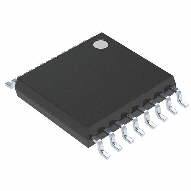


 工商网监
湘ICP备2023018690号
工商网监
湘ICP备2023018690号
