MBRA130LT3G,
NRVBA130LT3G
Surface Mount
Schottky Power Rectifier
SMA Power Surface Mount Package
www.onsemi.com
This device employs the Schottky Barrier principle in a
metal−to−silicon power rectifier. Features epitaxial construction with
oxide passivation and metal overlay contact. Ideally suited for low
voltage, high frequency switching power supplies; free wheeling
diodes and polarity protection diodes.
SCHOTTKY BARRIER
RECTIFIER
1.0 AMPERES, 30 VOLTS
Features
•
•
•
•
•
•
Compact Package with J−Bend Leads Ideal for Automated Handling
Highly Stable Oxide Passivated Junction
Guardring for Over−Voltage Protection
Low Forward Voltage Drop
NRVBA Prefix for Automotive and Other Applications Requiring
Unique Site and Control Change Requirements; AEC−Q101
Qualified and PPAP Capable*
These Devices are Pb−Free, Halogen Free/BFR Free and are RoHS
Compliant
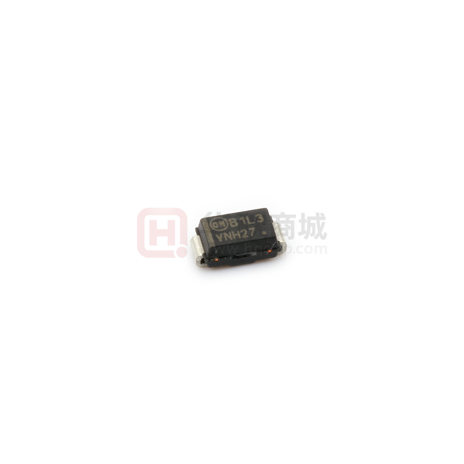
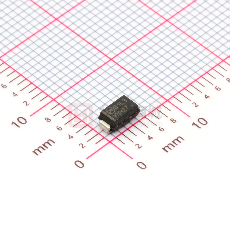
SMA
CASE 403D
PLASTIC
MARKING DIAGRAM
B1L3
AYWWG
Mechanical Characteristics:
•
•
•
•
•
•
•
•
Case: Molded Epoxy
Epoxy Meets UL 94 V−0 @ 0.125 in
Weight: 70 mg (approximately)
Finish: All External Surfaces Corrosion Resistant and Terminal
Leads are Readily Solderable
Lead and Mounting Surface Temperature for Soldering Purposes:
260°C Max. for 10 Seconds
Polarity: Cathode Lead Indicated by Either Notch in Plastic Body or
Polarity Band
Device Meets MSL1 Requirements
ESD Ratings:
♦ Machine Model = C (> 400 V)
♦ Human Body Model = 3B (> 8000 V)
B1L3
= Specific Device Code
A
= Assembly Location***
Y
= Year
WW
= Work Week
G
= Pb−Free Package
(Note: Microdot may be in either location)
***The Assembly Location code (A) is front side
optional. In cases where the Assembly Location is
stamped in the package bottom (molding ejecter pin),
the front side assembly code may be blank.
ORDERING INFORMATION
Package
Shipping†
MBRA130LT3G
SMA
(Pb−Free)
5,000 /
Tape & Reel **
NRVBA130LT3G*
SMA
(Pb−Free)
5,000 /
Tape & Reel **
Device
**
12 mm Tape, 13” Reel
†For information on tape and reel specifications,
including part orientation and tape sizes, please
refer to our Tape and Reel Packaging Specification
Brochure, BRD8011/D.
© Semiconductor Components Industries, LLC, 2012
April, 2017 − Rev. 9
1
Publication Order Number:
MBRA130LT3/D
�MBRA130LT3G, NRVBA130LT3G
MAXIMUM RATINGS
Rating
Peak Repetitive Reverse Voltage
Working Peak Reverse Voltage
DC Blocking Voltage
Average Rectified Forward Current
(At Rated VR, TC = 105°C)
Symbol
Value
Unit
VRRM
VRWM
VR
30
V
IO
1.0
A
Peak Repetitive Forward Current
(At Rated VR, Square Wave, 100 kHz, TC = 105°C)
IFRM
Non−Repetitive Peak Surge Current
(Surge Applied at Rated Load Conditions Halfwave, Single Phase, 60 Hz)
IFSM
Storage Temperature
Tstg
−55 to +150
TJ
−55 to +125
°C
dv/dt
10,000
V/ms
Operating Junction Temperature
Voltage Rate of Change, (Rated VR, TJ = 25°C)
2.0
25
A
A
°C
Stresses exceeding those listed in the Maximum Ratings table may damage the device. If any of these limits are exceeded, device functionality
should not be assumed, damage may occur and reliability may be affected.
THERMAL CHARACTERISTICS
Characteristic
Thermal Resistance — Junction−to−Lead (Note 1)
Thermal Resistance — Junction−to−Ambient (Note 1)
Symbol
Value
Unit
RqJL
RqJA
35
86
°C/W
1. Mounted on 2″ Square PC Board with 1″ Square Total Pad Size, PC Board FR4.
ELECTRICAL CHARACTERISTICS
Symbol
Characteristic
VF
Maximum Instantaneous Forward Voltage (Note 2)
(IF = 1.0 A) see Figure 2
(IF = 2.0 A)
IR
Maximum Instantaneous Reverse Current
(VR = 30 V) see Figure 4
(VR = 15 V)
Value
Unit
TJ = 25°C
TJ = 100°C
0.41
0.47
0.35
0.43
TJ = 25°C
TJ = 100°C
1.0
0.4
25
12
Volts
mA
Product parametric performance is indicated in the Electrical Characteristics for the listed test conditions, unless otherwise noted. Product
performance may not be indicated by the Electrical Characteristics if operated under different conditions.
2. Pulse Test: Pulse Width ≤ 250 ms, Duty Cycle ≤ 2.0%.
www.onsemi.com
2
�I F, INSTANTANEOUS FORWARD CURRENT (AMPS)
i F , INSTANTANEOUS FORWARD CURRENT (AMPS)
MBRA130LT3G, NRVBA130LT3G
10
TJ = 125°C
1.0
TJ = 85°C
TJ = 25°C
TJ = -40°C
0.1
0
0.2
0.4
0.6
0.8
1.0
TJ = 125°C
1.0
TJ = 85°C
TJ = 25°C
0.1
0
0.2
0.4
0.6
0.8
vF, INSTANTANEOUS FORWARD VOLTAGE (VOLTS)
VF, MAXIMUM INSTANTANEOUS FORWARD VOLTAGE (VOLTS)
Figure 1. Typical Forward Voltage
Figure 2. Maximum Forward Voltage
1.0
100E-3
I R , MAXIMUM REVERSE CURRENT (AMPS)
100E-3
I R , REVERSE CURRENT (AMPS)
10
10E-3
TJ = 125°C
1.0E-3
TJ = 85°C
100E-6
10E-3
1.0E-3
TJ = 85°C
TJ = 25°C
100E-6
10E-6
TJ = 25°C
1.0E-6
0
10
20
30
10E-6
1.0E-6
0
10
20
VR, REVERSE VOLTAGE (VOLTS)
VR, REVERSE VOLTAGE (VOLTS)
Figure 3. Typical Reverse Current
Figure 4. Maximum Reverse Current
www.onsemi.com
3
30
�MBRA130LT3G, NRVBA130LT3G
1.8
dc
1.6
1.4
SQUARE WAVE
1.2
1.0
Ipk/Io = p
0.8
Ipk/Io = 5
0.6
Ipk/Io = 10
0.4
Ipk/Io = 20
0.2
0
0
R (T) , TRANSIENT THERMAL RESISTANCE (NORMALIZED)
PFO , AVERAGE POWER DISSIPATION (WATTS)
FREQ = 20 kHz
20
40
60
80
100
120
0.6
dc
SQUARE WAVE
0.5
Ipk/Io = p
0.4
Ipk/Io = 5
Ipk/Io = 10
0.3
Ipk/Io = 20
0.2
0.1
0
140
0
0.2
0.4
0.6
0.8
1.0
1.2
1.4
TL, LEAD TEMPERATURE (°C)
IO, AVERAGE FORWARD CURRENT (AMPS)
Figure 5. Current Derating
Figure 6. Forward Power Dissipation
1.6
T, TIME (s)
1.0E+0
100E-3
10E-3
1.0E-3
100E-6
10E-6
100E-6
10E-3
1.0E-3
100E-3
10E+0
1.0E+0
T, TIME (s)
Figure 7. Thermal Response
1000
C, CAPACITANCE (pF)
IO , AVERAGE FORWARD CURRENT (AMPS)
2.0
TJ = 25°C
100
10
1.0
0
5.0
10
15
20
25
30
VR, REVERSE VOLTAGE (VOLTS)
Figure 8. Capacitance
www.onsemi.com
4
35
40
100E+0
1.0E+3
�MBRA130LT3G, NRVBA130LT3G
PACKAGE DIMENSIONS
SMA
CASE 403D
ISSUE H
HE
NOTES:
1. DIMENSIONING AND TOLERANCING PER ANSI Y14.5M,
1982.
2. CONTROLLING DIMENSION: INCH.
3. DIMENSION b SHALL BE MEASURED WITHIN DIMENSION L.
E
b
DIM
A
A1
b
c
D
E
HE
L
D
POLARITY INDICATOR
OPTIONAL AS NEEDED
(SEE STYLES)
MIN
1.97
0.05
1.27
0.15
2.29
4.06
4.83
0.76
MILLIMETERS
NOM
MAX
2.10
2.20
0.10
0.20
1.45
1.63
0.28
0.41
2.60
2.92
4.32
4.57
5.21
5.59
1.14
1.52
MIN
0.078
0.002
0.050
0.006
0.090
0.160
0.190
0.030
INCHES
NOM
0.083
0.004
0.057
0.011
0.103
0.170
0.205
0.045
MAX
0.087
0.008
0.064
0.016
0.115
0.180
0.220
0.060
A
L
A1
c
SOLDERING FOOTPRINT*
4.000
0.157
2.000
0.079
2.000
0.079
SCALE 8:1
mm Ǔ
ǒinches
*For additional information on our Pb−Free strategy and soldering
details, please download the ON Semiconductor Soldering and
Mounting Techniques Reference Manual, SOLDERRM/D.
ON Semiconductor and
are trademarks of Semiconductor Components Industries, LLC dba ON Semiconductor or its subsidiaries in the United States and/or other countries.
ON Semiconductor owns the rights to a number of patents, trademarks, copyrights, trade secrets, and other intellectual property. A listing of ON Semiconductor’s product/patent
coverage may be accessed at www.onsemi.com/site/pdf/Patent−Marking.pdf. ON Semiconductor reserves the right to make changes without further notice to any products herein.
ON Semiconductor makes no warranty, representation or guarantee regarding the suitability of its products for any particular purpose, nor does ON Semiconductor assume any liability
arising out of the application or use of any product or circuit, and specifically disclaims any and all liability, including without limitation special, consequential or incidental damages.
Buyer is responsible for its products and applications using ON Semiconductor products, including compliance with all laws, regulations and safety requirements or standards,
regardless of any support or applications information provided by ON Semiconductor. “Typical” parameters which may be provided in ON Semiconductor data sheets and/or
specifications can and do vary in different applications and actual performance may vary over time. All operating parameters, including “Typicals” must be validated for each customer
application by customer’s technical experts. ON Semiconductor does not convey any license under its patent rights nor the rights of others. ON Semiconductor products are not
designed, intended, or authorized for use as a critical component in life support systems or any FDA Class 3 medical devices or medical devices with a same or similar classification
in a foreign jurisdiction or any devices intended for implantation in the human body. Should Buyer purchase or use ON Semiconductor products for any such unintended or unauthorized
application, Buyer shall indemnify and hold ON Semiconductor and its officers, employees, subsidiaries, affiliates, and distributors harmless against all claims, costs, damages, and
expenses, and reasonable attorney fees arising out of, directly or indirectly, any claim of personal injury or death associated with such unintended or unauthorized use, even if such
claim alleges that ON Semiconductor was negligent regarding the design or manufacture of the part. ON Semiconductor is an Equal Opportunity/Affirmative Action Employer. This
literature is subject to all applicable copyright laws and is not for resale in any manner.
PUBLICATION ORDERING INFORMATION
LITERATURE FULFILLMENT:
Literature Distribution Center for ON Semiconductor
19521 E. 32nd Pkwy, Aurora, Colorado 80011 USA
Phone: 303−675−2175 or 800−344−3860 Toll Free USA/Canada
Fax: 303−675−2176 or 800−344−3867 Toll Free USA/Canada
Email: orderlit@onsemi.com
◊
N. American Technical Support: 800−282−9855 Toll Free
USA/Canada
Europe, Middle East and Africa Technical Support:
Phone: 421 33 790 2910
Japan Customer Focus Center
Phone: 81−3−5817−1050
www.onsemi.com
5
ON Semiconductor Website: www.onsemi.com
Order Literature: http://www.onsemi.com/orderlit
For additional information, please contact your local
Sales Representative
MBRA130LT3/D
�


 工商网监
湘ICP备2023018690号
工商网监
湘ICP备2023018690号
