MC10E131, MC100E131
5�V ECL 4‐Bit D Flip‐Flop
Description
The MC10E/100E131 is a quad master-slave D-type flip-flop with
differential outputs. Each flip-flop may be clocked separately by
holding Common Clock (CC) LOW and using the Clock Enable (CE)
inputs for clocking. Common clocking is achieved by holding the CE
inputs LOW and using CC to clock all four flip-flops. In this case, the
CE inputs perform the function of controlling the common clock, to
each flip-flop.
Individual asynchronous resets are provided (R). Asynchronous set
controls (S) are ganged together in pairs, with the pairing chosen to
reflect physical chip symmetry.
Data enters the master when both CC and CE are LOW, and transfers
to the slave when either CC or CE (or both) go HIGH.
The 100 Series contains temperature compensation.
Features
•
•
•
•
•
•
•
•
•
•
•
•
1100 MHz Min. Toggle Frequency
Differential Outputs
Individual and Common Clocks
Individual Resets (asynchronous)
Paired Sets (asynchronous)
PECL Mode Operating Range:
♦ VCC = 4.2 V to 5.7 V with VEE = 0 V
NECL Mode Operating Range:
♦ VCC = 0 V with VEE = −4.2 V to −5.7 V
Metastability Time Constant is 200 ps.
Internal Input 50 kW Pulldown Resistors
ESD Protection:
♦ Human Body Model; > 2 kV
♦ Machine Model; > 200 V
Meets or Exceeds JEDEC Spec EIA/JESD78 IC Latchup Test
Moisture Sensitivity Level: 3 (Pb-Free)
♦ For Additional Information, see Application Note AND8003/D
Flammability Rating:UL 94 V−0 @ 0.125 in, Oxygen Index: 28 to 34
•
• Transistor Count = 240 devices
• These Devices are Pb-Free, Halogen Free and are RoHS Compliant
www.onsemi.com
PLCC−28
FN SUFFIX
CASE 776−02
MARKING DIAGRAM*
1
MCxxxE131G
AWLYYWW
xxx
A
WL
YY
WW
G
= 10 or 100
= Assembly Location
= Wafer Lot
= Year
= Work Week
= Pb-Free Package
*For additional marking information, refer to
Application Note AND8002/D.
ORDERING INFORMATION
Device
Package
Shipping†
MC10E131FNG
PLCC−28
(Pb-Free)
37 Units/Tube
MC10E131FNR2G
PLCC−28
(Pb-Free)
500/Tape & Reel
MC100E131FNG
PLCC−28
(Pb-Free)
37 Units/Tube
MC100E131FNR2G
PLCC−28
(Pb-Free)
500/Tape & Reel
†For information on tape and reel specifications, including part orientation and tape sizes, please refer
to our Tape and Reel Packaging Specifications
Brochure, BRD8011/D.
© Semiconductor Components Industries, LLC, 2016
July, 2016 − Rev. 12
1
Publication Order Number:
MC10E131/D
�MC10E131, MC100E131
D3
D
CE3
R3
D2
CE2
R2
25
24
23
22
VCCO Q3
21
20
Q3
26
18
Q2
D2
D3
27
17
Q2
CE2
S12
28
16
VCC
VEE
1
15
Q1
CC
2
14
Q1
S03
3
13
Q0
D0
4
12
Q0
CE0
6
R0
7
8
9
10
D1
CE1
R1
NC
D
S
R
Q3
Q
Q3
Q
Q2
Q
Q2
Q
Q1
Q
Q1
Q
Q0
Q
Q0
R2
S03
S12
CC
R1
R
CE1
D1
11
D
S
R0
VCCO
R
CE0
* All VCC and VCCO pins are tied together on the die.
D0
Warning: All VCC, VCCO, and VEE pins must be externally
connected to Power Supply to guarantee proper operation.
Figure 1. Pinout Diagram
D
S
Figure 2. Logic Diagram
Table 1. PIN DESCRIPTION
PIN
D0 − D3
CE0 − CE3
R0 − R3
CC
S03, S12
Q0 − Q3, Q0 − Q3
VCC, VCCO
VEE
NC
Q
R3
CE3
5
R
19
Pinout: 28-Lead PLCC
(Top View)
S
FUNCTION
ECL Data Inputs
ECL Clock Enables (Individual)
ECL Resets
ECL Common Clock
ECL Sets (paired)
ECL Differential Outputs
Positive Supply
Negative Supply
No Connect
www.onsemi.com
2
�MC10E131, MC100E131
Table 2. MAXIMUM RATINGS
Symbol
Rating
Unit
VCC
PECL Mode Power Supply
Parameter
VEE = 0 V
Condition 1
Condition 2
8
V
VEE
NECL Mode Power Supply
VCC = 0 V
−8
V
VI
PECL Mode Input Voltage
NECL Mode Input Voltage
VEE = 0 V
VCC = 0 V
6
−6
V
Iout
Output Current
Continuous
Surge
50
100
mA
TA
Operating Temperature Range
0 to +85
°C
Tstg
Storage Temperature Range
−65 to +150
°C
qJA
Thermal Resistance (Junction-to-Ambient)
0 lfpm
500 lfpm
PLCC−28
63.5
43.5
°C/W
qJC
Thermal Resistance (Junction-to-Case)
Standard Board
PLCC−28
22 to 26
°C/W
Tsol
Wave Solder (Pb-Free)
265
°C
VI ≤ VCC
VI ≥ VEE
Stresses exceeding those listed in the Maximum Ratings table may damage the device. If any of these limits are exceeded, device functionality
should not be assumed, damage may occur and reliability may be affected.
Table 3. 10E SERIES PECL DC CHARACTERISTICS (VCCx = 5.0 V; VEE = 0.0 V (Note 1))
−40°C
Max
58
70
3980
4070
4160
Output LOW Voltage
(Note 2)
3050
3210
VIH
Input HIGH Voltage
3830
VIL
Input LOW Voltage
3050
IIH
Input HIGH Current
CC
S
R, CE
D
IIL
Input LOW Current
Characteristic
IEE
Power Supply Current
VOH
Output HIGH Voltage
(Note 2)
VOL
Typ
Max
58
70
Min
25°C
Typ
Symbol
Min
0°C
Typ
Max
58
70
4020
4105
4190
3370
3050
3210
3995
4160
3870
3285
3520
3050
350
450
300
150
Min
Typ
Max
Unit
58
70
mA
4090
4185
4280
mV
3370
3050
3227
3405
mV
4030
4190
3940
4110
4280
mV
3285
3520
3050
3302
3555
mV
350
450
300
150
0.5
85°C
0.3
Min
350
450
300
150
0.5
0.25
350
450
300
150
0.3
0.2
mA
mA
NOTE: Device will meet the specifications after thermal equilibrium has been established when mounted in a test socket or printed circuit
board with maintained transverse airflow greater than 500 lfpm. Electrical parameters are guaranteed only over the declared
operating temperature range. Functional operation of the device exceeding these conditions is not implied. Device specification limit
values are applied individually under normal operating conditions and not valid simultaneously.
1. Input and output parameters vary 1:1 with VCC. VEE can vary −0.46 V / +0.06 V.
2. Outputs are terminated through a 50ĂW resistor to VCC − 2.0 V.
www.onsemi.com
3
�MC10E131, MC100E131
Table 4. 10E SERIES NECL DC CHARACTERISTICS (VCCx = 0.0 V; VEE = −5.0 V (Note 1))
−40°C
Symbol
Characteristic
Min
0°C
Typ
Max
58
70
Min
25°C
Typ
Max
58
70
Min
85°C
Typ
Max
58
70
Min
Typ
Max
Unit
58
70
mA
IEE
Power Supply Current
VOH
Output HIGH Voltage
(Note 2)
−1020
−930
−840
−980
−895
−810
−910
−815
−720
mV
VOL
Output LOW Voltage
(Note 2)
−1950
−1790
−1630
−1950
−1790
−1630
−1950
−1773
−1595
mV
VIH
Input HIGH Voltage
−1170
−1005
−840
−1130
−970
−810
−1060
−890
−720
mV
VIL
Input LOW Voltage
−1950
−1715
−1480
−1950
−1715
−1480
−1950
−1698
−1445
mV
IIH
Input HIGH Current
CC
S
R, CE
D
IIL
Input LOW Current
350
450
300
150
350
450
300
150
0.5
0.3
350
450
300
150
0.5
0.065
350
450
300
150
0.3
0.2
mA
mA
NOTE: Device will meet the specifications after thermal equilibrium has been established when mounted in a test socket or printed circuit
board with maintained transverse airflow greater than 500 lfpm. Electrical parameters are guaranteed only over the declared
operating temperature range. Functional operation of the device exceeding these conditions is not implied. Device specification limit
values are applied individually under normal operating conditions and not valid simultaneously.
1. Input and output parameters vary 1:1 with VCC. VEE can vary −0.46 V / +0.06 V.
2. Outputs are terminated through a 50ĂW resistor to VCC − 2.0 V.
Table 5. 100E SERIES PECL DC CHARACTERISTICS (VCCx = 5.0 V; VEE = 0.0 V (Note 1))
−40°C
Symbol
Characteristic
IEE
Power Supply Current
VOH
Output HIGH Voltage
(Note 2)
VOL
Output LOW Voltage
(Note 2)
VIH
Input HIGH Voltage
VIL
Input LOW Voltage
IIH
Input HIGH Current
CC
S
R, CE
D
IIL
Input LOW Current
Min
0°C
Typ
Max
58
70
Min
25°C
Typ
Max
58
70
3975
4050
4120
3190
3295
3975
3835
3355
3190
Typ
Max
58
70
3975
4050
4120
3380
3190
3255
3975
4120
3835
3355
3525
3190
350
450
300
150
Min
Typ
Max
Unit
67
81
mA
3975
4050
4120
mV
3380
3190
3260
3380
mV
3975
4120
3835
3975
4120
mV
3355
3525
3190
3355
3525
mV
350
450
300
150
0.5
85°C
0.3
Min
350
450
300
150
0.5
0.25
350
450
300
150
0.5
0.2
mA
mA
NOTE: Device will meet the specifications after thermal equilibrium has been established when mounted in a test socket or printed circuit
board with maintained transverse airflow greater than 500 lfpm. Electrical parameters are guaranteed only over the declared
operating temperature range. Functional operation of the device exceeding these conditions is not implied. Device specification limit
values are applied individually under normal operating conditions and not valid simultaneously.
1. Input and output parameters vary 1:1 with VCC. VEE can vary −0.46 V / +0.8 V.
2. Outputs are terminated through a 50ĂW resistor to VCC − 2.0 V.
www.onsemi.com
4
�MC10E131, MC100E131
Table 6. 100E SERIES NECL DC CHARACTERISTICS (VCCx = 0.0 V; VEE = −5.0 V (Note 1))
−40°C
Symbol
Characteristic
IEE
Power Supply Current
VOH
Output HIGH Voltage
(Note 2)
VOL
Output LOW Voltage
(Note 2)
VIH
Input HIGH Voltage
VIL
Input LOW Voltage
IIH
Input HIGH Current
CC
S
R, CE
D
IIL
Input LOW Current
Min
0°C
Typ
Max
58
70
Min
25°C
Typ
Max
58
70
−1025
−950
−880
−1810
−1705
−1620
−1025
−1165
−1025
−1645
−1810
−1645
350
450
300
150
Min
Typ
Max
58
70
−1025
−950
−880
−1810
−1745
−1620
−880
−1165
−1025
−1475
−1810
−1645
350
450
300
150
0.5
85°C
0.3
Min
Typ
Max
Unit
67
81
mA
−1025
−950
−880
mV
−1810
−1740
−1620
mV
−880
−1165
−1025
−880
mV
−1475
−1810
−1645
−1475
mV
350
450
300
150
0.5
0.25
350
450
300
150
0.5
0.2
mA
mA
NOTE: Device will meet the specifications after thermal equilibrium has been established when mounted in a test socket or printed circuit
board with maintained transverse airflow greater than 500 lfpm. Electrical parameters are guaranteed only over the declared
operating temperature range. Functional operation of the device exceeding these conditions is not implied. Device specification limit
values are applied individually under normal operating conditions and not valid simultaneously.
1. Input and output parameters vary 1:1 with VCC. VEE can vary −0.46 V / +0.8 V.
2. Outputs are terminated through a 50ĂW resistor to VCC − 2.0 V.
Table 7. AC CHARACTERISTICS (VCCx = 5.0 V; VEE = 0.0 V or VCCx = 0.0 V; VEE = −5.0 V (Note 1))
−40°C
Symbol
Characteristic
Min
Typ
fMAX
Maximum Toggle Frequency
1100
1400
tPLH
tPHL
Propagation Delay to Output
CE
CC
R
S
310
275
400
300
600
600
635
550
25°C
Max
750
725
875
775
Min
Typ
1100
1400
360
325
450
350
500
500
640
550
85°C
Max
700
675
825
725
Min
Typ
1100
1400
360
325
450
350
500
500
640
550
Max
Unit
MHz
700
675
825
725
ps
tS
Setup Time (Note 2)
D
200
20
150
20
150
20
ps
tH
Hold Time (Note 2)
D
225
−20
175
−20
175
−20
ps
tRR
Reset Recovery Time
450
150
400
150
400
150
ps
tPW
Minimum Pulse Width
CLK
R, S
400
400
tSKEW
Within-Device Skew (Note 3)
tJITTER
Random Clock Jitter
tr/tf
Rise/Fall Time (20−80%)
275
400
400
ps
400
400
60
60
60
ps
很抱歉,暂时无法提供与“MC100E131FNR2”相匹配的价格&库存,您可以联系我们找货
免费人工找货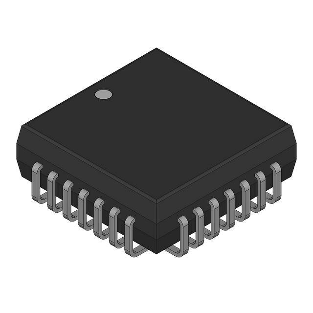


 工商网监
湘ICP备2023018690号
工商网监
湘ICP备2023018690号
