MC100EL38
5�V ECL ÷2, ÷4/6 Clock
Generation Chip
Description
The MC100EL38 is a low skew ÷2, ÷4/6 clock generation chip
designed explicitly for low skew clock generation applications. The
internal dividers are synchronous to each other, therefore, the common
www.onsemi.com
output edges are all precisely aligned. The device can be driven by
either a differential or single-ended ECL or, if positive power supplies
are used, PECL input signal.
The VBB pin, an internally generated voltage supply, is available to
this device only. For single-ended input conditions, the unused
differential input is connected to VBB as a switching reference voltage.
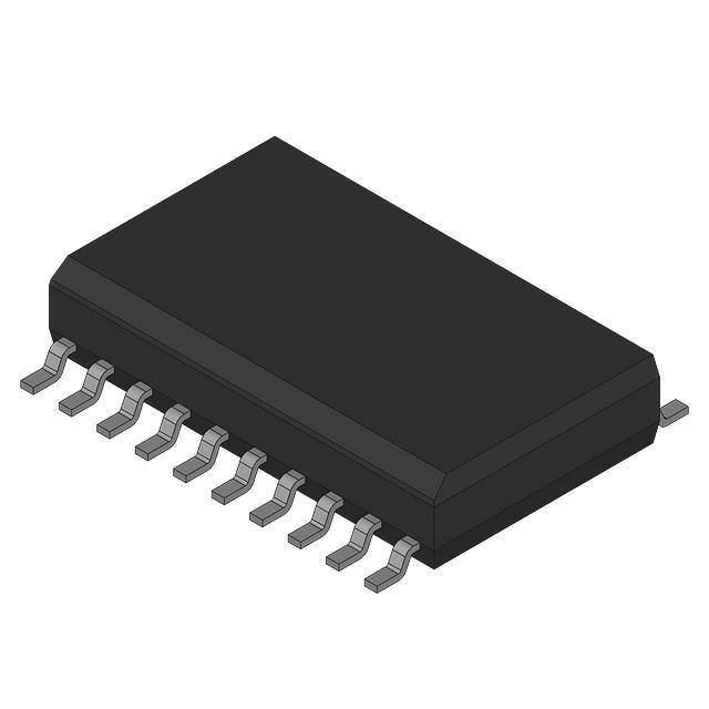
SOIC−20 WB
VBB may also rebias AC coupled inputs. When used, decouple VBB
DW SUFFIX
and VCC via a 0.01 mF capacitor and limit current sourcing or sinking
CASE 751D−05
to 0.5 mA. When not used, VBB should be left open.
The common enable (EN) is synchronous so that the internal
dividers will only be enabled/disabled when the internal clock is
MARKING DIAGRAM*
already in the LOW state. This avoids any chance of generating a runt
20
clock pulse on the internal clock when the device is enabled/disabled
as can happen with an asynchronous control. An internal runt pulse
could lead to losing synchronization between the internal divider
100EL38
AWLYYWWG
stages. The internal enable flip-flop is clocked on the falling edge of
the input clock, therefore, all associated specification limits are
referenced to the negative edge of the clock input.
1
The Phase_Out output will go HIGH for one clock cycle whenever
A
= Assembly Location
the ÷2 and the ÷4/6 outputs are both transitioning from a LOW to a
WL
=
Wafer Lot
HIGH. This output allows for clock synchronization within the system.
YY
= Year
Upon startup, the internal flip-flops will attain a random state;
WW
= Work Week
therefore, for systems which utilize multiple EL38s, the master reset
G
= Pb-Free Package
(MR) input must be asserted to ensure synchronization. For systems
*For additional marking information, refer to
which only use one EL38, the MR pin need not be exercised as the
Application Note AND8002/D.
internal divider design ensures synchronization between the ÷2 and
the ÷4/6 outputs of a single device.
• 50 ps Output-to-Output Skew
ORDERING INFORMATION
• Synchronous Enable/Disable
Device
Package
Shipping†
• Master Reset for Synchronization
MC100EL38DWR2G SOIC−20 WB 1000/Tape & Reel
• ESD Protection:
(Pb-Free)
♦ 2 kV Human Body Model
♦ 100 V Machine Model
†For information on tape and reel specifications, including part orientation and tape sizes, please refer
• The 100 Series Contains Temperature Compensation
to our Tape and Reel Packaging Specifications
• PECL Mode Operating Range:
Brochure, BRD8011/D.
♦ VCC = 4.2 V to 5.7 V with VEE = 0 V
• NECL Mode Operating Range:
• Moisture Sensitivity Level: 3 (Pb-Free)
♦ VCC = 0 V with VEE = −4.2 V to −5.7 V
♦ For Additional Information, see Application Note
AND8003/D
• Internal 75 kW Input Pulldown Resistors on CLK, EN,
• Flammability Rating:
MR, and DIVSEL
♦ UL 94 V−0 @ 0.125 in, Oxygen Index: 28 to 34
• Q Output will Default LOW with Inputs Open or at
• Transistor Count = 388 devices
VEE
• Meets or Exceeds JEDEC Spec EIA/JESD78 IC
• These Devices are Pb-Free, Halogen Free and are
Latchup Test
RoHS Compliant
© Semiconductor Components Industries, LLC, 2016
July, 2016 − Rev. 9
1
Publication Order Number:
MC100EL38/D
�MC100EL38
VCC
Q0
Q0
Q1
Q1
Q2
Q2
Q3
Q3
VEE
20
19
18
17
16
15
14
13
12
11
1
2
3
4
5
6
7
8
9
10
CLK
VBB
MR
VCC
EN DIV_SEL CLK
VCC Phase_Out Phase_Out
* All VCC pins are tied together on the die.
Warning: All VCC and VEE pins must be externally connected
to Power Supply to guarantee proper operation.
Figure 1. Pinout Assignment (Top View)
Q0
CLK
P2
CLK
R
Q0
Q1
Q1
Q2
EN
R
P4/6
Q2
R
Q3
MR
Q3
DIVSEL
PHASE_OUT
Phase
Out
R Logic
PHASE_OUT
Figure 2. Logic Diagram
Table 1. PIN DESCRIPTION
Pin
Table 2. FUNCTION TABLE
Function
CLK, CLK
ECL Diff Clock Inputs
Q0, Q1; Q0, Q1
ECL Diff ÷2 Outputs
Q2, Q3; Q2, Q3
ECL Diff ÷4/6 Outputs
EN
ECL Sync Enable Input
MR
ECL Master Reset Input
DIVSEL
ECL Frequency Select Input
Phase_Out, Phase_Out
ECL Phase Sync Diff. Signal Output
VBB
Reference Voltage Output
VCC
Positive Supply
VEE
Negative Supply
CLK
EN
MR
Z
ZZ
X
L
H
X
L
L
H
Function
Divide
Hold Q0−3
Reset Q0−3
Z = Low-to-High Transition
ZZ = High-to-Low Transition
X = Don’t Care
DIVSEL
L
H
www.onsemi.com
2
Q2, Q3 OUTPUTS
Divide by 4
Divide by 6
�MC100EL38
Table 3. MAXIMUM RATINGS
Symbol
Rating
Unit
VCC
PECL Mode Power Supply
Parameter
VEE = 0 V
Condition 1
Condition 2
8
V
VEE
NECL Mode Power Supply
VCC = 0 V
−8
V
VI
PECL Mode Input Voltage
NECL Mode Input Voltage
VEE = 0 V
VCC = 0 V
6
−6
V
Iout
Output Current
Continuous
Surge
50
100
MA
IBB
VBB Sink/Source
± 0.5
mA
TA
Operating Temperature Range
−40 to +85
°C
Tstg
Storage Temperature Range
−65 to +150
°C
qJA
Thermal Resistance (Junction-to-Ambient)
0 lfpm
500 lfpm
SOIC−20 WB
90
60
°C/W
qJC
Thermal Resistance (Junction-to-Case)
Standard Board
SOIC−20 WB
30 to 35
°C/W
Tsol
Wave Solder (Pb-Free)
很抱歉,暂时无法提供与“MC100EL38DWR2G”相匹配的价格&库存,您可以联系我们找货
免费人工找货