ON Semiconductor
Is Now
To learn more about onsemi™, please visit our website at
www.onsemi.com
onsemi and and other names, marks, and brands are registered and/or common law trademarks of Semiconductor Components Industries, LLC dba “onsemi” or its affiliates and/or
subsidiaries in the United States and/or other countries. onsemi owns the rights to a number of patents, trademarks, copyrights, trade secrets, and other intellectual property. A listing of onsemi
product/patent coverage may be accessed at www.onsemi.com/site/pdf/Patent-Marking.pdf. onsemi reserves the right to make changes at any time to any products or information herein, without
notice. The information herein is provided “as-is” and onsemi makes no warranty, representation or guarantee regarding the accuracy of the information, product features, availability, functionality,
or suitability of its products for any particular purpose, nor does onsemi assume any liability arising out of the application or use of any product or circuit, and specifically disclaims any and all
liability, including without limitation special, consequential or incidental damages. Buyer is responsible for its products and applications using onsemi products, including compliance with all laws,
regulations and safety requirements or standards, regardless of any support or applications information provided by onsemi. “Typical” parameters which may be provided in onsemi data sheets and/
or specifications can and do vary in different applications and actual performance may vary over time. All operating parameters, including “Typicals” must be validated for each customer application
by customer’s technical experts. onsemi does not convey any license under any of its intellectual property rights nor the rights of others. onsemi products are not designed, intended, or authorized
for use as a critical component in life support systems or any FDA Class 3 medical devices or medical devices with a same or similar classification in a foreign jurisdiction or any devices intended for
implantation in the human body. Should Buyer purchase or use onsemi products for any such unintended or unauthorized application, Buyer shall indemnify and hold onsemi and its officers, employees,
subsidiaries, affiliates, and distributors harmless against all claims, costs, damages, and expenses, and reasonable attorney fees arising out of, directly or indirectly, any claim of personal injury or death
associated with such unintended or unauthorized use, even if such claim alleges that onsemi was negligent regarding the design or manufacture of the part. onsemi is an Equal Opportunity/Affirmative
Action Employer. This literature is subject to all applicable copyright laws and is not for resale in any manner. Other names and brands may be claimed as the property of others.
�MC10EP446, MC100EP446
3.3 V/5 V 8‐Bit
CMOS/ECL/TTL Data Input
Parallel/Serial Converter
Description
The MC10/100EP446 is an integrated 8−bit parallel to serial data
converter. The device is designed with unique circuit topology to
operate for NRZ data rates up to 3.2 Gb/s. The conversion sequence
from parallel data into a serial data stream is from bit D0 to D7. The
parallel input pins D0−D7 are configurable to be threshold controlled by
CMOS, ECL, or TTL level signals. The serial data rate output can be
selected at internal clock data rate or twice the internal clock data rate
using the CKSEL pin.
Control pins are provided to reset (SYNC) and disable internal clock
circuitry (CKEN). In either CKSEL modes, the internal flip−flops are
triggered on the rising edge for CLK and the multiplexers are switched
on the falling edge of CLK, therefore, all associated specification
limits are referenced to the negative edge of the clock input.
Additionally, VBB pin is provided for single−ended input condition.
The 100 Series devices contain temperature compensation network.
•
•
•
•
•
3.2 Gb/s Typical Data Rate Capability
Differential Clock and Serial Outputs
VBB Output for Single-ended Input Applications
Asynchronous Data Reset (SYNC)
PECL Mode Operating Range:
VCC = 3.0 V to 5.5 V with VEE = 0 V
NECL Mode Operating Range:
VCC = 0 V with VEE = −3.0 V to −5.5 V
Open Input Default State
Safety Clamp on Inputs
Parallel Interface Can Support PECL, TTL or CMOS
These Devices are Pb−Free and are RoHS Compliant
© Semiconductor Components Industries, LLC, 2014
June, 2014 − Rev. 11
MARKING
DIAGRAM*
MCxxx
EP446
AWLYYWWG
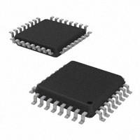
LQFP−32
FA SUFFIX
CASE 873A
1
1
32
QFN32
MN SUFFIX
CASE 488AM
Features
•
•
•
•
•
http://onsemi.com
MCxxx
EP446
AWLYYWWG
G
xxx
= 10 or 100
A
= Assembly Location
WL
= Wafer Lot
YY
= Year
WW
= Work Week
G or G = Pb−Free Package
(Note: Microdot may be in either location)
*For additional marking information, refer to
Application Note AND8002/D.
ORDERING INFORMATION
See detailed ordering and shipping information in the package
dimensions section on page 18 of this data sheet.
1
Publication Order Number:
MC10EP446/D
�D6
D7
18
D5
D6
19
D4
D5
20
D3
D4
21
D2
D3
22
D1
D2
23
D0
D1
24
D7
D0
MC10EP446, MC100EP446
24
23
22
21
20
19
18
17
17
VCC
25
16
VEE
VCC
25
16
VEE
VCF
26
15
PCLK
VCF
26
15
PCLK
VEF
27
14
PCLK
VEF
27
14
PCLK
VEE
28
13
VCC
VEE
28
13
VCC
SYNC
29
12
SOUT SYNC
29
12
SOUT
SYNC
30
11
SOUT SYNC
30
11
SOUT
VBB2
31
10
VCC
VBB2
31
10
VCC
VCC
32
9
VCC
VCC
32
9
VCC
7
8
VCC
VEE
CKEN
CKEN
VBB1
CLK
CLK
CKSEL
VCC
1
2
3
4
5
6
7
8
VEE
6
CKEN
5
CKEN
4
VBB1
3
CLK
2
CLK
1
Exposed Pad (EP)
CKSEL
MC10EP446
MC100EP446
Warning: All VCC and VEE pins must be externally connected
to Power Supply to guarantee proper operation.
Figure 2. QFN−32 Pinout (Top View)
Figure 1. LQFP−32 Pinout (Top View)
Table 1. PIN DESCRIPTION
PIN
FUNCTION
D0*−D7*
ECL, CMOS, or TTL Parallel Data Input
SOUT, SOUT
ECL Differential Serial Data Output
CLK*, CLK*
ECL Differential Clock Input
PCLK, PCLK
ECL Differential Parallel Clock Output
SYNC*, SYNC**
ECL Conversion Synchronizing Differential Input (Reset)***
CKSEL*
ECL Clock Input Selector
CKEN*, CKEN*
ECL Clock Enable Differential Input
VCF
ECL, CMOS, or TTL Input Selector
VEF
ECL Reference Mode Connection
VBB1, VBB2
Reference Voltage Output
VCC
Positive Supply
VEE
Negative Supply
* Pins will default LOW when left open.
**Pins will default HIGH when left open.
***The rising edge of SYNC will asynchronously reset the internal circuitry. The falling edge of the SYNC followed by the falling edge of CLK
initiates the conversion process synchronously on the next rising edge of CLK.
http://onsemi.com
2
�MC10EP446, MC100EP446
Table 2. TRUTH TABLE
Function
HIGH
Pin
CKSEL
LOW
SOUT: PCLK = 8:1
CLK: SOUT = 1:1
SOUT: PCLK = 8:1
CLK: SOUT = 1:2
CLK
CLK
SOUT
SOUT
CKEN
Synchronously Disables Normal Parallel to Serial
Conversion
Synchronously Enables Normal Parallel to Serial Conversion
SYNC
Asynchronously Resets Internal Flip−Flops*
Synchronous Enable
*The rising edge of SYNC will asynchronously reset the internal circuitry. The falling edge of the SYNC followed by the falling edge of CLK initiates
the conversion process synchronously on the next rising edge of CLK.
Table 3. INPUT VOLTAGE LEVEL SELECTION TABLE
Input Function
Connect To VCF Pin
ECL Mode
VEF Pin
Table 4. DATA INPUT OPERATING VOLTAGE TABLE
Power Supply
(VCC,VEE)
Data Inputs (D [0:7])
CMOS
TTL
PECL
NECL
CMOS Mode
No Connect
PECL
p
p
p
N/A
TTL Mode*
1.5 V $ 100 mV
NECL
N/A
N/A
N/A
p
*For TTL Mode, if no external voltage can be provided, the reference
voltage can be provided by connecting the appropriate resistor
between VCF and VEE pins.
Power Supply
Resistor Value 10% (Tolerance)
3.3 V
1.5 kW
5.0 V
500 W
http://onsemi.com
3
�MC10EP446, MC100EP446
D0
D
Q
CR
MUX
2:1
D
Q
CR
D4
D
Q
CR
MUX
2:1
D
Q
C R
D2
D
Q
C R
MUX
2:1
D
Q
CR
D6
D
Q
CR
D1
D
MUX
2:1
SOUT
SOUT
Q
CR
MUX
2:1
D
Q
CR
D5
D
Q
CR
MUX
2:1
D
Q
CR
D3
D
Q
CR
MUX
2:1
D
Q
CR
D7
D
Q
CR
÷2
÷2
÷2
CKEN
CKEN
CLK
CLK
D
Q
C R
CKSEL
SYNC
SYNC
VCC
VEE
VBB
VCF
VEF
Figure 3. Logic Diagram
http://onsemi.com
4
MUX
2:1
Control
Logic
PCLK
PCLK
�MC10EP446, MC100EP446
Table 5. ATTRIBUTES
Characteristics
Value
Internal Input Pulldown Resistor
75 kW
Internal Input Pullup Resistor
ESD Protection
37.5 kW
Human Body Model
Machine Model
Charged Device Model
> 2 kV
> 100 V
> 2 kV
Moisture Sensitivity, Indefinite Time Out of Drypack (Note 1)
LQFP−32
QFN−32
Flammability Rating
Oxygen Index: 28 to 34
Pb Pkg
Pb−Free Pkg
Level 2
−
Level 2
Level 1
UL 94 V−0 @ 0.125 in
Transistor Count
962 Devices
Meets or exceeds JEDEC Spec EIA/JESD78 IC Latchup Test
1. For additional information, see Application Note AND8003/D.
Table 6. MAXIMUM RATINGS
Symbol
Parameter
Condition 1
Condition 2
Rating
Unit
VCC
PECL Mode Power Supply
VEE = 0 V
6
V
VEE
NECL Mode Power Supply
VCC = 0 V
−6
V
VI
PECL Mode Input Voltage
NECL Mode Input Voltage
VEE = 0 V
VCC = 0 V
6
−6
V
Iout
Output Current
Continuous
Surge
50
100
mA
IBB
VBB Sink/Source
± 0.5
mA
TA
Operating Temperature Range
−40 to +85
°C
Tstg
Storage Temperature Range
−65 to +150
°C
qJA
Thermal Resistance (Junction−to−Ambient)
0 lfpm
500 lfpm
LQFP−32
LQFP−32
80
55
°C/W
qJC
Thermal Resistance (Junction−to−Case)
Standard Board
LQFP−32
12 to 17
°C/W
qJA
Thermal Resistance (Junction−to−Ambient)
0 lfpm
500 lfpm
QFN−32
QFN−32
31
27
°C/W
qJC
Thermal Resistance (Junction−to−Case)
2S2P
QFN−32
12
°C/W
Tsol
Wave Solder


 工商网监
湘ICP备2023018690号
工商网监
湘ICP备2023018690号
