MC34166, MC33166
Inverting Switching
Regulators - Step-Up/Down
3.0 A
The MC34166, MC33166 series are high performance fixed
frequency power switching regulators that contain the primary
functions required for dc−to−dc converters. This series was specifically
designed to be incorporated in step−down and voltage−inverting
configurations with a minimum number of external components and
can also be used cost effectively in step−up applications.
These devices consist of an internal temperature compensated
reference, fixed frequency oscillator with on−chip timing components,
latching pulse width modulator for single pulse metering, high gain
error amplifier, and a high current output switch.
Protective features consist of cycle−by−cycle current limiting,
undervoltage lockout, and thermal shutdown. Also included is a low
power standby mode that reduces power supply current to 36 mA.
http://onsemi.com
x
A
WL
Y
WW
G
= 3 or 4
= Assembly Location
= Wafer Lot
= Year
= Work Week
= Pb−Free Package
Features
•
•
•
•
•
•
•
•
•
•
•
•
•
•
Output Switch Current in Excess of 3.0 A
Fixed Frequency Oscillator (72 kHz) with On−Chip Timing
Provides 5.05 V Output without External Resistor Divider
Precision 2% Reference
0% to 95% Output Duty Cycle
Cycle−by−Cycle Current Limiting
Undervoltage Lockout with Hysteresis
Internal Thermal Shutdown
Operation from 7.5 V to 40 V
Standby Mode Reduces Power Supply Current to 36 mA
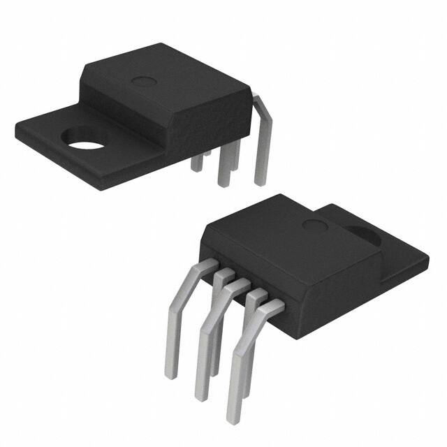
Economical 5−Lead TO−220 Package with Two Optional Leadforms
Also Available in Surface Mount D2PAK Package
Moisture Sensitivity Level (MSL) Equals 1
Pb−Free Packages are Available
1
MARKING
DIAGRAMS
TO−220
TH SUFFIX
CASE 314A
MC
3x166T
AWLYWWG
TO−220
TV SUFFIX
CASE 314B
MC
3x166T
AWLYWWG
5
1
5
Heatsink surface connected to Pin 3
Vin
4
ILIMIT
Oscillator
TO−220
T SUFFIX
CASE 314D
1
S
Q
2
R
5
Pin
PWM
UVLO
Thermal
L
1.
2.
3.
4.
5.
Reference
1
VO
5.05 V/
3.0 A
5
This device contains 143 active transistors.
September, 2019 − Rev. 7
1
MC
3x166T
AWLYWWG
5
Heatsink surface (shown as
terminal 6 in case outline
drawing) is connected to Pin 3
1
5
ORDERING INFORMATION
Figure 1. Simplified Block Diagram
(Step Down Application)
© Semiconductor Components Industries, LLC, 2005
Voltage Feedback Input
Switch Output
Ground
Input Voltage/VCC
Compensation/Standby
D2PAK
D2T SUFFIX
CASE 936A
EA
3
MC
3x166T
AWLYWWG
See detailed ordering and shipping information in the package
dimensions section on page 2 of this data sheet.
1
Publication Order Number:
MC34166/D
�MC34166, MC33166
ORDERING INFORMATION
Device
Operating
Temperature Range
Shipping†
Package
MC33166D2T
D2PAK − Surface Mount
MC33166D2TG
D2PAK − Surface Mount
(Pb−Free)
MC33166D2TR4
D2PAK − Surface Mount
MC33166D2TR4G
D2PAK − Surface Mount
(Pb−Free)
MC33166T
MC33166TG
800 / Tape & Reel
TO−220 − Straight Lead
TA= −40° to +85°C
TO−220 − Straight Lead
(Pb−Free)
MC33166TH
TO−220 − Horizontal Mount
MC33166THG
TO−220 − Horizontal Mount
(Pb−Free)
MC33166TV
TO−220 − Vertical Mount
MC33166TVG
TO−220 − Vertical Mount
(Pb−Free)
MC34166D2T
D2PAK − Surface Mount
MC34166D2TG
D2PAK − Surface Mount
(Pb−Free)
MC34166D2TR4
D2PAK − Surface Mount
MC34166D2TR4G
D2PAK − Surface Mount
(Pb−Free)
MC34166T
MC34166TG
50 Units/Rail
50 Units/Rail
800 / Tape & Reel
TO−220 − Straight Lead
TA= 0° to +70°C
TO−220 − Straight Lead
(Pb−Free)
MC34166TH
TO−220 − Horizontal Mount
MC34166THG
TO−220 − Horizontal Mount
(Pb−Free)
MC34166TV
TO−220 − Vertical Mount
MC34166TVG
TO−220 − Vertical Mount
(Pb−Free)
50 Units/Rail
†For information on tape and reel specifications, including part orientation and tape sizes, please refer to our Tape and Reel Packaging
Specifications Brochure, BRD8011/D.
MAXIMUM RATINGS
Rating
Power Supply Input Voltage
Switch Output Voltage Range
Voltage Feedback and Compensation Input Voltage Range
Power Dissipation
Case 314A, 314B and 314D (TA = +25°C)
Thermal Resistance, Junction−to−Ambient
Thermal Resistance, Junction−to−Case
Case 936A (D2PAK) (TA = +25°C)
Thermal Resistance, Junction−to−Ambient
Thermal Resistance, Junction−to−Case
Operating Junction Temperature
Operating Ambient Temperature (Note 2)
MC34166
MC33166
Symbol
Value
Unit
VCC
40
V
VO(switch)
−1.5 to + Vin
V
VFB, VComp
−1.0 to + 7.0
V
PD
qJA
qJC
PD
qJA
qJC
Internally Limited
65
5.0
Internally Limited
70
5.0
W
°C/W
°C/W
W
°C/W
°C/W
TJ
+150
°C
TA
0 to + 70
− 40 to + 85
°C
Storage Temperature Range
Tstg
− 65 to +150
°C
Maximum ratings are those values beyond which device damage can occur. Maximum ratings applied to the device are individual stress limit
values (not normal operating conditions) and are not valid simultaneously. If these limits are exceeded, device functional operation is not implied,
damage may occur and reliability may be affected.
1. This device series contains ESD protection and exceeds the following tests:
Human Body Model 2000 V per MIL−STD−883, Method 3015.
Machine Model Method 200 V.
2. Tlow = 0°C for MC34166
Thigh = + 70°C for MC34166
= − 40°C for MC33166
= + 85°C for MC33166
http://onsemi.com
2
�MC34166, MC33166
ELECTRICAL CHARACTERISTICS (VCC = 12 V, for typical values TA = +25°C, for min/max values TA is the operating ambient
temperature range that applies [Notes 3, 4], unless otherwise noted.)
Symbol
Min
Typ
Max
Unit
TA = +25°C
TA = Tlow to Thigh
fOSC
65
62
72
−
79
81
kHz
TA = +25°C
TA = Tlow to Thigh
VFB(th)
4.95
4.85
5.05
−
5.15
5.2
V
Regline
−
0.03
0.078
%/V
Characteristic
OSCILLATOR
Frequency (VCC = 7.5 V to 40 V)
ERROR AMPLIFIER
Voltage Feedback Input Threshold
Line Regulation (VCC = 7.5 V to 40 V, TA = +25°C)
Input Bias Current (VFB = VFB(th) + 0.15 V)
Power Supply Rejection Ratio (VCC = 10 V to 20 V, f = 120 Hz)
Output Voltage Swing
High State (ISource = 75 mA, VFB = 4.5 V)
Low State (ISink = 0.4 mA, VFB = 5.5 V)
IIB
−
0.15
1.0
mA
PSRR
60
80
−
dB
VOH
VOL
4.2
−
4.9
1.6
−
1.9
DC(max)
DC(min)
92
0
95
0
100
0
Vsat
−
(VCC −1.5)
(VCC −1.8)
V
V
PWM COMPARATOR
Duty Cycle
Maximum (VFB = 0 V)
Minimum (VComp = 1.9 V)
%
SWITCH OUTPUT
Output Voltage Source Saturation (VCC = 7.5 V, ISource = 3.0 A)
Off−State Leakage (VCC = 40 V, Pin 2 = GND)
Isw(off)
−
0
100
mA
Ipk(switch)
3.3
4.3
6.0
A
tr
tf
−
−
100
50
200
100
Startup Threshold (VCC Increasing, TA = +25°C)
Vth(UVLO)
5.5
5.9
6.3
V
Hysteresis (VCC Decreasing, TA = +25°C)
VH(UVLO)
0.6
0.9
1.2
V
−
−
36
31
100
55
mA
mA
Current Limit Threshold
ns
Switching Times (VCC = 40 V, Ipk = 3.0 A, L = 375 mH, TA = +25°C)
Output Voltage Rise Time
Output Voltage Fall Time
UNDERVOLTAGE LOCKOUT
TOTAL DEVICE
Power Supply Current (TA = +25°C )
Standby (VCC = 12 V, VComp < 0.15 V)
Operating (VCC = 40 V, Pin 1 = GND for maximum duty cycle)
ICC
3. Low duty cycle pulse techniques are used during test to maintain junction temperature as close to ambient as possible.
Thigh = + 70°C for MC34166
4. Tlow = 0°C for MC34166
= − 40°C for MC33166
= + 85°C for MC33166
http://onsemi.com
3
�MC34166, MC33166
100
VCC = 12 V
VFB(th) Max = 5.15 V
IIB, INPUT BIAS CURRENT (nA)
V FB(th), VOLTAGE FEEDBACK INPUT THRESHOLD (V)
5.25
5.17
5.09
VFB(th) Typ = 5.05 V
5.01
VFB(th) Min = 4.95 V
4.93
4.85
-�55
-�25
0
25
50
75
TA, AMBIENT TEMPERATURE (°C)
100
VCC = 12 V
VFB = VFB(th)
80
60
40
20
0
-�55
125
80
Gain
VCC = 12 V
VComp = 3.25 V
RL = 100 k
TA = +25°C
0
30
60
60
40
90
Phase
φ, EXCESS PHASE (DEGREES)
A VOL, OPEN LOOP VOLTAGE GAIN (dB)
100
20
120
0
150
-�20
10
100
1.0 k
10 k
100 k
f, FREQUENCY (Hz)
180
10 M
1.0 M
125
1.6
1.2
0.8
VCC = 12 V
VFB = 5.5 V
TA = +25°C
0.4
0
0
0.4
0.8
1.2
1.6
ISink, OUTPUT SINK CURRENT (mA)
2.0
Figure 5. Error Amp Output Saturation
versus Sink Current
4.0
100
DC, SWITCH OUTPUT DUTY CYCLE (%)
Δ f OSC , OSCILLATOR FREQUENCY CHANGE (%)
100
2.0
Figure 4. Error Amp Open Loop Gain and
Phase versus Frequency
VCC = 12 V
0
-�4.0
-�8.0
-�12
-�55
0
25
50
75
TA, AMBIENT TEMPERATURE (°C)
Figure 3. Voltage Feedback Input Bias
Current versus Temperature
Vsat , OUTPUT SATURATION VOLTAGE (V)
Figure 2. Voltage Feedback Input Threshold
versus Temperature
-�25
-�25
0
25
50
75
100
TA, AMBIENT TEMPERATURE (°C)
80
60
40
20
0
1.5
125
VCC = 12 V
TA = +25°C
Figure 6. Oscillator Frequency Change
versus Temperature
2.0
2.5
3.0
3.5
4.0
VComp, COMPENSATION VOLTAGE (V)
Figure 7. Switch Output Duty Cycle
versus Compensation Voltage
http://onsemi.com
4
4.5
�0
0
VCC
Vsw, SWITCH OUTPUT VOLTAGE (V)
Vsat , SWITCH OUTPUT SOURCE SATURATION (V)
MC34166, MC33166
-�0.5
TA = +25°C
-1.0
-1.5
-�2.0
-�2.5
-�3.0
0
1.0
2.0
3.0
4.0
ISource, SWITCH OUTPUT SOURCE CURRENT (A)
GND
VCC = 12 V
Pin 5 = 2.0 V
Pins 1, 3 = GND
Pin 2 Driven Negative
-�0.2
-�0.4
Isw = 100 mA
-�0.6
-�0.8
Isw = 10 mA
-1.0
-1.2
-�55
5.0
VCC = 12 V
Pins 1, 2, 3 = GND
4.5
4.3
4.1
-�25
0
25
50
75
TA, AMBIENT TEMPERATURE (°C)
100
120
80
40
0
0
125
10
20
30
VCC, SUPPLY VOLTAGE (V)
40
Figure 11. Standby Supply Current
versus Supply Voltage
6.5
40
Startup Threshold
VCC Increasing
6.0
I CC, SUPPLY CURRENT (mA)
Vth(UVLO) , UNDERVOLTAGE LOCKOUT THRESHOLD (V)
125
Pin 4 = VCC
Pins 1, 3, 5 = GND
Pin 2 Open
TA = +25°C
Figure 10. Switch Output Current Limit
Threshold versus Temperature
5.5
Turn-Off Threshold
VCC Decreasing
5.0
4.5
4.0
-�55
100
160
4.7
3.9
-�55
0
25
50
75
TA, AMBIENT TEMPERATURE (°C)
Figure 9. Negative Switch Output Voltage
versus Temperature
I CC, SUPPLY CURRENT ( μ A)
I pk(switch) , CURRENT LIMIT THRESHOLD (A)
Figure 8. Switch Output Source Saturation
versus Source Current
-�25
30
20
Pin 4 = VCC
Pins 1, 3 = GND
Pins 2, 5 Open
TA = +25°C
10
0
-�25
0
25
50
75
TA, AMBIENT TEMPERATURE (°C)
100
125
0
Figure 12. Undervoltage Lockout
Threshold versus Temperature
10
20
30
VCC, SUPPLY VOLTAGE (V)
Figure 13. Operating Supply Current
versus Supply Voltage
http://onsemi.com
5
40
�MC34166, MC33166
Vin
Current
Sense
+
4
Input Voltage/VCC
Cin
Oscillator
S
CT
Switch
Output
Q
R
Pulse Width
Modulator
2
Undervoltage
Lockout
PWM Latch
Thermal
Shutdown
L
5.05 V
Reference
+
+
Error
Amp
100 mA
1
120
GND
3
Compensation
=
5
Voltage
Feedback
Input
CF
RF
Sink Only
Positive True Logic
Figure 14. MC34166 Representative Block Diagram
4.1 V
Timing Capacitor CT
Compensation
2.3 V
ON
Switch Output
OFF
Figure 15. Timing Diagram
http://onsemi.com
6
R2
R1
VO
CO
�MC34166, MC33166
INTRODUCTION
input is biased to the internal 5.05 V reference and is not
pinned out. The reference has an accuracy of ± 2.0% at room
temperature. To provide 5.0 V at the load, the reference is
programmed 50 mV above 5.0 V to compensate for a 1.0%
voltage drop in the cable and connector from the converter
output. If the converter design requires an output voltage
greater than 5.05 V, resistor R1 must be added to form a
divider network at the feedback input as shown in Figures 14
and 19. The equation for determining the output voltage with
the divider network is:
The MC34166, MC33166 series are monolithic power
switching regulators that are optimized for dc−to−dc
converter applications. These devices operate as fixed
frequency, voltage mode regulators containing all the active
functions required to directly implement step−down and
voltage−inverting converters with a minimum number of
external components. They can also be used cost effectively
in step−up converter applications. Potential markets include
automotive, computer, industrial, and cost sensitive
consumer products. A description of each section of the
device is given below with the representative block diagram
shown in Figure 14.
Vout + 5.05
ǒRR2 ) 1Ǔ
1
External loop compensation is required for converter
stability. A simple low−pass filter is formed by connecting a
resistor (R2) from the regulated output to the inverting input,
and a series resistor−capacitor (RF, CF) between Pins 1 and 5.
The compensation network component values shown in each
of the applications circuits were selected to provide stability
over the tested operating conditions. The step−down converter
(Figure 19) is the easiest to compensate for stability. The
step−up (Figure 21) and voltage−inverting (Figure 23)
configurations operate as continuous conduction flyback
converters, and are more difficult to compensate. The simplest
way to optimize the compensation network is to observe the
response of the output voltage to a step load change, while
adjusting RF and CF for critical damping. The final circuit
should be verified for stability under four boundary conditions.
These conditions are minimum and maximum input voltages,
with minimum and maximum loads.
By clamping the voltage on the error amplifier output
(Pin 5) to less than 150 mV, the internal circuitry will be
placed into a low power standby mode, reducing the power
supply current to 36 mA with a 12 V supply voltage. Figure 11
illustrates the standby supply current versus supply voltage.
The Error Amplifier output has a 100 mA current source
pullup that can be used to implement soft−start. Figure 18
shows the current source charging capacitor CSS through a
series diode. The diode disconnects CSS from the feedback
loop when the 1.0 M resistor charges it above the operating
range of Pin 5.
Oscillator
The oscillator frequency is internally programmed to
72 kHz by capacitor CT and a trimmed current source. The
charge to discharge ratio is controlled to yield a 95%
maximum duty cycle at the Switch Output. During the
discharge of CT, the oscillator generates an internal blanking
pulse that holds the inverting input of the AND gate high,
disabling the output switch transistor. The nominal oscillator
peak and valley thresholds are 4.1 V and 2.3 V respectively.
Pulse Width Modulator
The Pulse Width Modulator consists of a comparator with
the oscillator ramp voltage applied to the noninverting input,
while the error amplifier output is applied into the inverting
input. Output switch conduction is initiated when CT is
discharged to the oscillator valley voltage. As CT charges to
a voltage that exceeds the error amplifier output, the latch
resets, terminating output transistor conduction for the
duration of the oscillator ramp−up period. This PWM/Latch
combination prevents multiple output pulses during a given
oscillator clock cycle. Figures 7 and 15 illustrate the switch
output duty cycle versus the compensation voltage.
Current Sense
The MC34166 series utilizes cycle−by−cycle current
limiting as a means of protecting the output switch transistor
from overstress. Each on−cycle is treated as a separate
situation. Current limiting is implemented by monitoring the
output switch transistor current buildup during conduction, and
upon sensing an overcurrent condition, immediately turning
off the switch for the duration of the oscillator ramp−up period.
The collector current is converted to a voltage by an internal
trimmed resistor and compared against a reference by the
Current Sense comparator. When the current limit threshold is
reached, the comparator resets the PWM latch. The current
limit threshold is typically set at 4.3 A. Figure 10 illustrates
switch output current limit threshold versus temperature.
Switch Output
The output transistor is designed to switch a maximum of
40 V, with a minimum peak collector current of 3.3 A. When
configured for step−down or voltage−inverting applications, as
in Figures 19 and 23, the inductor will forward bias the output
rectifier when the switch turns off. Rectifiers with a high
forward voltage drop or long turn−on delay time should not be
used. If the emitter is allowed to go sufficiently negative,
collector current will flow, causing additional device heating
and reduced conversion efficiency. Figure 9 shows that by
clamping the emitter to 0.5 V, the collector current will be in
the range of 100 mA over temperature. A 1N5822 or
Error Amplifier and Reference
A high gain Error Amplifier is provided with access to the
inverting input and output. This amplifier features a typical dc
voltage gain of 80 dB, and a unity gain bandwidth of 600 kHz
with 70 degrees of phase margin (Figure 4). The noninverting
http://onsemi.com
7
�MC34166, MC33166
Thermal Protection
equivalent Schottky barrier rectifier is recommended to fulfill
these requirements.
Internal Thermal Shutdown circuitry is provided to protect
the integrated circuit in the event that the maximum junction
temperature is exceeded. When activated, typically at 170°C,
the latch is forced into a ‘reset’ state, disabling the output
switch. This feature is provided to prevent catastrophic
failures from accidental device overheating. It is not
intended to be used as a substitute for proper heatsinking.
The MC34166 is contained in a 5−lead TO−220 type package.
The tab of the package is common with the center pin (Pin 3)
and is normally connected to ground.
Undervoltage Lockout
An Undervoltage Lockout comparator has been
incorporated to guarantee that the integrated circuit is fully
functional before the output stage is enabled. The internal
5.05 V reference is monitored by the comparator which
enables the output stage when VCC exceeds 5.9 V. To prevent
erratic output switching as the threshold is crossed, 0.9 V of
hysteresis is provided.
DESIGN CONSIDERATIONS
Do not attempt to construct a converter on wire−wrap
or plug−in prototype boards. Special care should be taken
to separate ground paths from signal currents and ground
paths from load currents. All high current loops should be
kept as short as possible using heavy copper runs to minimize
ringing and radiated EMI. For best operation, a tight
component layout is recommended. Capacitors CIN, CO, and
all feedback components should be placed as close to the IC
as physically possible. It is also imperative that the Schottky
diode connected to the Switch Output be located as close to
the IC as possible.
+
Error
Amp
100 mA
+
Error
Amp
100 mA
120
1
120
Compensation
Compensation
1
5
R1
5
R1
I = Standby Mode
VShutdown = VZener + 0.7
Figure 17. Over Voltage Shutdown Circuit
Figure 16. Low Power Standby Circuit
+
Error
Amp
100 mA
1
120
Compensation
D2
5
R1
D1
Vin
1.0 M
Css
tSoft-Start ≈ 35,000 Css
Figure 18. Soft−Start Circuit
http://onsemi.com
8
�MC34166, MC33166
Vin
12 V
+
4
ILIMIT
+
Oscillator
Cin
330
S
Q1
Q
R
2
PWM
D1
1N5822
UVLO
L
190 mH
Thermal
Reference
+
+
EA
R2
1
5
3
Test
CF
RF
0.1
68 k
CO
2200
6.8 k
VO
5.05 V/3.0 A
+
R1
Conditions
Results
Line Regulation
Vin = 8.0 V to 36 V, IO = 3.0 A
5.0 mV = ± 0.05%
Load Regulation
Vin = 12 V, IO = 0.25 A to 3.0 A
2.0 mV = ± 0.02%
Output Ripple
Vin = 12 V, IO = 3.0 A
10 mVpp
Short Circuit Current
Vin = 12 V, RL = 0.1 W
4.3 A
Efficiency
Vin = 12 V, IO = 3.0 A
82.8%
L = Coilcraft M1496−A or General Magnetics Technology GMT−0223, 42 turns of #16 AWG
on Magnetics Inc. 58350−A2 core. Heatsink = AAVID Engineering Inc. 5903B, or 5930B.
The Step−Down Converter application is shown in Figure 19. The output switch transistor Q1 interrupts the input voltage, generating a
squarewave at the LCO filter input. The filter averages the squarewaves, producing a dc output voltage that can be set to any level between
Vin and Vref by controlling the percent conduction time of Q1 to that of the total oscillator cycle time. If the converter design requires an output
voltage greater than 5.05 V, resistor R1 must be added to form a divider network at the feedback input.
Figure 19. Step−Down Converter
+
-
+
ÉÉÉÉÉ
ÉÉÉÉÉ
ÉÉÉÉÉ
ÉÉÉÉÉ
ÉÉÉÉÉ
ÉÉÉ
+
R2
-
VO
CO
Vin
1.9 ″
+
(Bottom View)
D1
R1
L
CF
RF
Cin
MC34166 STEP−DOWN
3.0″
(Top View)
Figure 20. Step−Down Converter Printed Circuit Board and Component Layout
http://onsemi.com
9
�MC34166, MC33166
Vin
12 V
+
4
ILIMIT
+
Oscillator
Cin
330
S
D1
1N5822
Q1
Q
R
2
PWM
L
190 mH
UVLO
*RG
620
D4
1N4148
Thermal
Q2
MTP3055EL
Reference
+
D3
1N967A
+
D2
1N5822
EA
R2
1
5
3
CF
RF
0.47
4.7 k
CO
1000
6.8 k
VO
28 V/0.6 A
+
R1
1.5 k
*Gate resistor RG, zener diode D3, and diode D4 are required only when Vin is greater than 20 V.
Test
Conditions
Results
Line Regulation
Vin = 8.0 V to 24 V, IO = 0.6 A
23 mV = ± 0.41%
Load Regulation
Vin = 12 V, IO = 0.1 A to 0.6 A
3.0 mV = ± 0.005%
Output Ripple
Vin = 12 V, IO = 0.6 A
100 mVpp
Short Circuit Current
Vin = 12 V, RL = 0.1 W
4.0 A
Efficiency
Vin = 12 V, IO = 0.6 A
82.8%
L = Coilcraft M1496−A or General Magnetics Technology GMT−0223, 42 turns of #16 AWG
on Magnetics Inc. 58350−A2 core.
Heatsink = AAVID Engineering Inc. MC34166: 5903B, or 5930B MTP3055EL: 5925B
Figure 21 shows that the MC34166 can be configured as a step−up/down converter with the addition of an external power MOSFET. Energy
is stored in the inductor during the on−time of transistors Q1 and Q2. During the off−time, the energy is transferred, with respect to ground, to
the output filter capacitor and load. This circuit configuration has two significant advantages over the basic step−up converter circuit. The first
advantage is that output short−circuit protection is provided by the MC34166, since Q1 is directly in series with Vin and the load. Second, the
output voltage can be programmed to be less than Vin. Notice that during the off−time, the inductor forward biases diodes D1 and D2, transferring
its energy with respect to ground rather than with respect to Vin. When operating with Vin greater than 20 V, a gate protection network is required
for the MOSFET. The network consists of components RG, D3, and D4.
Figure 21. Step−Up/Down Converter
D3
ÎÎÎÎÎ
ÎÎÎÎÎ
ÎÎÎÎÎ
ÎÎÎÎÎ
ÎÎÎÎÎ
ÎÎÎ
+
+
(Bottom View)
CF
R1
+
D1
Cin
RF
D2
(Top View)
Figure 22. Step−Up/Down Converter Printed Circuit Board and Component Layout
http://onsemi.com
10
ÎÎ
ÎÎÎ
ÎÎ
ÎÎÎÎ
ÎÎ
Q2
-
-
CO
Vin
L
+
VO
R2
1.9″
MC34166 STEP−UP/DOWN
3.45″
RG
�MC34166, MC33166
Vin
12 V
+
4
ILIMIT
+
Oscillator
Cin
330
S
Q1
Q
R
2
PWM
L
190 mH
UVLO
D1
1N5822
Thermal
Reference
+
+
EA
R1
1
Test
CF
RF
0.47
4.7 k
VO
-12 V/1.0 A
CO
2200
+
5
3
2.4 k
C1
R2
3.3 k
Conditions
0.047
Results
Line Regulation
Vin = 8.0 V to 24 V, IO = 1.0 A
3.0 mV = ± 0.01%
Load Regulation
Vin = 12 V, IO = 0.1 A to 1.0 A
4.0 mV = ± 0.017%
Output Ripple
Vin = 12 V, IO = 1.0 A
80 mVpp
Short Circuit Current
Vin = 12 V, RL = 0.1 W
3.74 A
Efficiency
Vin = 12 V, IO = 1.0 A
81.2%
L = Coilcraft M1496−A or General Magnetics Technology GMT−0223, 42 turns of #16 AWG
on Magnetics Inc. 58350−A2 core. Heatsink = AAVID Engineering Inc. 5903B, or 5930B.
Two potential problems arise when designing the standard voltage−inverting converter with the MC34166. First, the Switch Output emitter is
limited to −1.5 V with respect to the ground pin and second, the Error Amplifier’s noninverting input is internally committed to the reference and
is not pinned out. Both of these problems are resolved by connecting the IC ground pin to the converter’s negative output as shown in Figure 23.
This keeps the emitter of Q1 positive with respect to the ground pin and has the effect of reversing the Error Amplifier inputs. Note that the voltage
drop across R1 is equal to 5.05 V when the output is in regulation.
Figure 23. Voltage−Inverting Converter
3.0″
+
+
ÎÎÎÎÎ
ÎÎÎÎÎ
ÎÎÎÎÎ
ÎÎÎÎÎ
ÎÎÎÎÎ
ÎÎÎ
Cin
CF
+
+
(Bottom View)
L
RF
D1
R2
-
+
R1
C1
+
Vin
CO
VO
-
1.9 ″
MC34166
VOLTAGE-INVERTING
+
(Top View)
Figure 24. Voltage−Inverting Converter Printed Circuit Board and Component Layout
http://onsemi.com
11
+
�MC34166, MC33166
Vin
24 V
+
4
ILIMIT
+
Oscillator
1000
S
Q
R
2
PWM
1N5822
UVLO
MUR110
+
Thermal
T1
Reference
+
MUR110
VO3
1000 -12 V/100 mA
VO2
+
1000 12 V/300 mA
+
EA
6.8 k
1
1000
+
VO1
5.05 V/2.0 A
5
3
0.1
Tests
68 k
Conditions
Results
Line Regulation
5.0 V
12 V
−12 V
Vin = 15 V to 30 V, IO1 = 2.0 A, IO2 = 300 mA, IO3 = 100 mA
4.0 mV = ± 0.04%
450 mV = ±1.9%
350 mV = ±1.5%
Load Regulation
5.0 V
12 V
−12 V
Vin = 24 V, IO1 = 500 mA to 2.0 A, IO2 = 300 mA, IO3 = 100 mA
Vin = 24 V, IO1 = 2.0 A, IO2 = 100 mA to 300 mA, IO3 = 100 mA
Vin = 24 V, IO1 = 2.0 A, IO2 = 300 mA, IO3 = 30 mA to 100 mA
2.0 mV = ± 0.02%
420 mV = ±1.7%
310 mV = ±1.3%
Output Ripple
5.0 V
12 V
−12 V
Vin = 24 V, IO1 = 2.0 A, IO2 = 300 mA, IO3 = 100 mA
50 mVpp
25 mVpp
10 mVpp
Short Circuit Current
5.0 V
12 V
−12 V
Vin = 24 V, RL = 0.1 W
4.3 A
1.83 A
1.47 A
Vin = 24 V, IO1 = 2.0 A, IO2 = 300 mA, IO3 = 100 mA
83.3%
Efficiency
TOTAL
T1 = Primary: Coilcraft M1496-A or General Magnetics Technology GMT−0223, 42 turns of #16 AWG on Magnetics Inc. 58350-A2 core.
T1 = Secondary: VO2 − 65 turns of #26 AWG
T1 = Secondary: VO3 − 96 turns of #28 AWG
Heatsink = AAVID Engineering Inc. 5903B, or 5930B.
Multiple auxiliary outputs can easily be derived by winding secondaries on the main output inductor to form a transformer. The secondaries must
be connected so that the energy is delivered to the auxiliary outputs when the Switch Output turns off. During the OFF time, the voltage across
the primary winding is regulated by the feedback loop, yielding a constant Volts/Turn ratio. The number of turns for any given secondary voltage
can be calculated by the following equation:
# TURNS(SEC) +
VO(SEC) ) VF(SEC)
VO(PRI))VF(PRI)
#TURNS(PRI)
ǒ
Ǔ
Note that the 12 V winding is stacked on top of the 5.0 V output. This reduces the number of secondary turns and improves lead regulation. For
best auxiliary regulation, the auxiliary outputs should be less than 33% of the total output power.
Figure 25. Triple Output Converter
http://onsemi.com
12
�MC34166, MC33166
+
4
ILIMIT
Oscillator
22
0.01
1N5822
S
Q1
Q
R
Ǔ
2
UVLO
PWM
ǒ
VO + 5.05
������R1 ) 0.7
R2
L
D1
Thermal
+
EA
5
3
+
0.22
Z1
2N3906
1
470 k
R2
5.1 k
0.002
Vin
-12 V
1000
+
R1
36 k
MTP
3055E
Reference
+
VO
+�36 V/0.25 A
MUR415
R1
*Gate resistor RG, zener diode D3, and diode D4 are required only when Vin is greater than 20 V.
Test
Conditions
Results
Line Regulation
Vin = −10 V to − 20 V, IO = 0.25 A
250 mV = ± 0.35%
Load Regulation
Vin = −12 V, IO = 0.025 A to 0.25 A
790 mV = ±1.19%
Output Ripple
Vin = −12 V, IO = 0.25 A
80 mVpp
Efficiency
Vin = −12 V, IO = 0.25 A
79.2%
L = Coilcraft M1496−A or ELMACO CHK1050, 42 turns of #16 AWG on Magnetics Inc.
58350−A2 core.
Heatsink = AAVID Engineering Inc. 5903B or 5930B
Figure 26. Negative Input/Positive Output Regulator
+
Vin
18 V
4
ILIMIT
+
Oscillator
1000
S
Q
R
UVLO
2
PWM
Brush
Motor
Thermal
Reference
+
EA
1N5822
+
1
5.6 k
1.0 k
+
47
5
3
Test
0.1
Conditions
56 k
Results
Low Speed Line Regulation
Vin = 12 V to 24 V
1760 RPM ±1%
High Speed Line Regulation
Vin = 12 V to 24 V
3260 RPM ± 6%
Figure 27. Variable Motor Speed Control with EMF Feedback Sensing
http://onsemi.com
13
50 k
Faster
1000
�MC34166, MC33166
0.001
T1
MBR20100CT
+
1000
0.001
1N5404
MC34166
Step-Down
Converter
+
Output 1
0.001
RFI
115 VAC Filter
+
220
MJE13005
MBR20100CT
0.047
1N4937
100k
T2
+
1000
0.01
50
0.001
MC34166
Step-Down
Converter
+
MC34166
Step-Down
Converter
+
Output 2
0.001
3.3
+
100
1N4003
MBR20100CT
+
1000
0.001
T1 =
T1 =
T1 =
T1 =
T1 =
Core and Bobbin - Coilcraft PT3595
Primary - 104 turns #26 AWG
Base Drive - 3 turns #26 AWG
Secondaries - 16 turns #16 AWG
Total Gap - 0.002″
Output 3
T2 = Core - TDK T6 x 1.5 x 3 H5C2
T2 = 14 turns center tapped #30 AWG
T2 = Heatsink = AAVID Engineering Inc.
T2 = MC34166 and MJE13005 - 5903B
T2 = MBR20100CT - 5925B
The MC34166 can be used cost effectively in off−line applications even though it is limited to a maximum input voltage of 40 V. Figure 28 shows
a simple and efficient method for converting the AC line voltage down to 24 V. This preconverter has a total power rating of 125 W with a conversion
efficiency of 90%. Transformer T1 provides output isolation from the AC line and isolation between each of the secondaries. The circuit
self−oscillates at 50 kHz and is controlled by the saturation characteristics of T2. Multiple MC34166 post regulators can be used to provide
accurate independently regulated outputs for a distributed power system.
JUNCTION‐TO‐AIR ( °C/W)
R θ JA, THERMAL RESISTANCE
80
3.5
PD(max) for TA = +50°C
70
3.0
Free Air
Mounted
Vertically
60
ÎÎÎÎ
ÎÎÎÎ
ÎÎÎÎ
ÎÎÎÎ
2.0 oz. Copper
L
Minimum
Size Pad
50
2.5
2.0
L
40
1.5
RqJA
30
1.0
0
5.0
10
15
20
25
30
L, LENGTH OF COPPER (mm)
Figure 29. D2PAK Thermal Resistance and Maximum
Power Dissipation versus P.C.B. Copper Length
http://onsemi.com
14
PD, MAXIMUM POWER DISSIPATION (W)
Figure 28. Off−Line Preconverter
�MC34166, MC33166
Table 1. Design Equations
Calculation
Step−Down
Step−Up/Down
Voltage−Inverting
ton
toff
(Notes 1, 2)
Vout ) VF
Vin * Vsat * Vout
Vout ) VF1 ) VF2
Vin * VsatQ1 * VsatQ2
|Vout| ) VF
Vin * Vsat
ton
ton
toff
ton
fosc
)1
toff
ton
toff
ton
fosc
)1
toff
ton
toff
ton
fosc
)1
toff
Duty Cycle
(Note 3)
ton fosc
ton fosc
ton fosc
IL avg
Iout
t
Iout on ) 1
toff
t
Iout on ) 1
toff
Ipk(switch)
DI
IL avg ) L
2
DI
IL avg ) L
2
DI
IL avg ) L
2
L
ǒVin * VDIsatL * VoutǓton
* VsatQ2
ǒVin * VsatQ1
Ǔton
DIL
ǒVin *DILVsatǓton
Vripple(pp)
ǒ
DIL
Ǹǒ
Ǔ
ǒ
Ǔ
1
2 ) (ESR)2
8foscCo
ǒ
ǒ
Ǔ
Ǔ
ǒtton
) 1Ǔ Ǹǒ 1 Ǔ2 ) (ESR)2
foscCo
off
Ǔ
ǒ
Ǔ
ǒ
ǒ
Ǔ
Ǔ
ǒtton
) 1Ǔ Ǹǒ 1 Ǔ2 ) (ESR)2
foscCo
off
ǒ
Ǔ
R
R
R
Vref 2 ) 1
Vref 2 ) 1
Vref 2 ) 1
R1
R1
R1
1. Vsat − Switch Output source saturation voltage, refer to Figure 8.
2. VF − Output rectifier forward voltage drop. Typical value for 1N5822 Schottky barrier rectifier is 0.5 V.
3. Duty cycle is calculated at the minimum operating input voltage and must not exceed the guaranteed minimum DC(max) specification of 0.92.
Vout
The following converter characteristics must be chosen:
Vout − Desired output voltage.
Iout − Desired output current.
DIL − Desired peak−to−peak inductor ripple current. For maximum output current especially when the duty cycle is greater than
0.5, it is suggested that DIL be chosen to be less than 10% of the average inductor current IL avg. This will help prevent
Ipk(switch) from reaching the guaranteed minimum current limit threshold of 3.3 A. If the design goal is to use a minimum
inductance value, let DIL = 2 (IL avg). This will proportionally reduce the converter’s output current capability.
Vripple(pp) − Desired peak−to−peak output ripple voltage. For best performance, the ripple voltage should be kept to less than 2% of Vout.
Capacitor CO should be a low equivalent series resistance (ESR) electrolytic designed for switching regulator applications.
http://onsemi.com
15
�MECHANICAL CASE OUTLINE
PACKAGE DIMENSIONS
5 LEAD TO−220 (THA5)
CASE 314A−03
ISSUE E
DATE 09/29/2000
SCALE 1:1
−T−
B
−P−
Q
C
E
OPTIONAL
CHAMFER
A
U
F
L
G
5X
D
M
T P
K
5X
S
0.014 (0.356)
NOTES:
1. DIMENSIONING AND TOLERANCING PER ANSI
Y14.5M, 1982.
2. CONTROLLING DIMENSION: INCH.
3. DIMENSION D DOES NOT INCLUDE
INTERCONNECT BAR (DAMBAR) PROTRUSION.
DIMENSION D INCLUDING PROTRUSION SHALL
NOT EXCEED 0.043 (1.092) MAXIMUM.
SEATING
PLANE
M
J
DIM
A
B
C
D
E
F
G
J
K
L
Q
S
U
INCHES
MIN
MAX
0.572
0.613
0.390
0.415
0.170
0.180
0.025
0.038
0.048
0.055
0.570
0.585
0.067 BSC
0.015
0.025
0.730
0.745
0.320
0.365
0.140
0.153
0.210
0.260
0.468
0.505
MILLIMETERS
MIN
MAX
14.529 15.570
9.906 10.541
4.318
4.572
0.635
0.965
1.219
1.397
14.478 14.859
1.702 BSC
0.381
0.635
18.542 18.923
8.128
9.271
3.556
3.886
5.334
6.604
11.888 12.827
XX
XXXXXXXXX
AWLYWW
DOCUMENT NUMBER:
DESCRIPTION:
98ASB42217B
5 LEAD TO−220, THA5
Electronic versions are uncontrolled except when accessed directly from the Document Repository.
Printed versions are uncontrolled except when stamped “CONTROLLED COPY” in red.
PAGE 1 OF 1
ON Semiconductor and
are trademarks of Semiconductor Components Industries, LLC dba ON Semiconductor or its subsidiaries in the United States and/or other countries.
ON Semiconductor reserves the right to make changes without further notice to any products herein. ON Semiconductor makes no warranty, representation or guarantee regarding
the suitability of its products for any particular purpose, nor does ON Semiconductor assume any liability arising out of the application or use of any product or circuit, and specifically
disclaims any and all liability, including without limitation special, consequential or incidental damages. ON Semiconductor does not convey any license under its patent rights nor the
rights of others.
© Semiconductor Components Industries, LLC, 2019
www.onsemi.com
�MECHANICAL CASE OUTLINE
PACKAGE DIMENSIONS
TO−220 5 LEAD OFFSET
CASE 314B−05
ISSUE L
DATE 01/07/1994
SCALE 1:1
Q
OPTIONAL
CHAMFER
E
A
U
K
L
S
W
F
5X
G
5X
D
0.10 (0.254)
NOTES:
1. DIMENSIONING AND TOLERANCING PER ANSI
Y14.5M, 1982.
2. CONTROLLING DIMENSION: INCH.
3. DIMENSION D DOES NOT INCLUDE
INTERCONNECT BAR (DAMBAR) PROTRUSION.
DIMENSION D INCLUDING PROTRUSION SHALL
NOT EXCEED 0.043 (1.092) MAXIMUM.
C
B
−P−
M
T P
0.24 (0.610)
J
M
H
T
N
M
−T−
STYLE 1 THRU 4:
CANCELLED
DOCUMENT NUMBER:
DESCRIPTION:
V
98ASB42218B
TO−220 5 LEAD OFFSET
SEATING
PLANE
STYLE 5:
PIN 1.
2.
3.
4.
5.
DIM
A
B
C
D
E
F
G
H
J
K
L
N
Q
S
U
V
W
INCHES
MIN
MAX
0.572
0.613
0.390
0.415
0.170
0.180
0.025
0.038
0.048
0.055
0.850
0.935
0.067 BSC
0.166 BSC
0.015
0.025
0.900
1.100
0.320
0.365
0.320 BSC
0.140
0.153
--0.620
0.468
0.505
--0.735
0.090
0.110
MILLIMETERS
MIN
MAX
14.529 15.570
9.906 10.541
4.318
4.572
0.635
0.965
1.219
1.397
21.590 23.749
1.702 BSC
4.216 BSC
0.381
0.635
22.860 27.940
8.128
9.271
8.128 BSC
3.556
3.886
--- 15.748
11.888 12.827
--- 18.669
2.286
2.794
GATE
MIRROR
DRAIN
KELVIN
SOURCE
Electronic versions are uncontrolled except when accessed directly from the Document Repository.
Printed versions are uncontrolled except when stamped “CONTROLLED COPY” in red.
PAGE 1 OF 1
ON Semiconductor and
are trademarks of Semiconductor Components Industries, LLC dba ON Semiconductor or its subsidiaries in the United States and/or other countries.
ON Semiconductor reserves the right to make changes without further notice to any products herein. ON Semiconductor makes no warranty, representation or guarantee regarding
the suitability of its products for any particular purpose, nor does ON Semiconductor assume any liability arising out of the application or use of any product or circuit, and specifically
disclaims any and all liability, including without limitation special, consequential or incidental damages. ON Semiconductor does not convey any license under its patent rights nor the
rights of others.
© Semiconductor Components Industries, LLC, 2019
www.onsemi.com
�MECHANICAL CASE OUTLINE
PACKAGE DIMENSIONS
TO−220 5−LEAD
CASE 314D−04
ISSUE H
−T−
B
−Q−
B1
DETAIL A-A
A
U
SCALE 1:1
SEATING
PLANE
C
L
1234 5
K
D
E
DATE 29 JAN 2010
J
H
G
5 PL
0.356 (0.014)
M
T Q
M
B
B1
NOTES:
1. DIMENSIONING AND TOLERANCING PER ANSI
Y14.5M, 1982.
2. CONTROLLING DIMENSION: INCH.
3. DIMENSION D DOES NOT INCLUDE
INTERCONNECT BAR (DAMBAR) PROTRUSION.
DIMENSION D INCLUDING PROTRUSION SHALL
NOT EXCEED 10.92 (0.043) MAXIMUM.
INCHES
MIN
MAX
0.572
0.613
0.390
0.415
0.375
0.415
0.170
0.180
0.025
0.038
0.048
0.055
0.067 BSC
0.087
0.112
0.015
0.025
0.977
1.045
0.320
0.365
0.140
0.153
0.105
0.117
DIM
A
B
B1
C
D
E
G
H
J
K
L
Q
U
MILLIMETERS
MIN
MAX
14.529 15.570
9.906 10.541
9.525 10.541
4.318
4.572
0.635
0.965
1.219
1.397
1.702 BSC
2.210
2.845
0.381
0.635
24.810 26.543
8.128
9.271
3.556
3.886
2.667
2.972
STYLE 1 THRU 4:
1. OBSOLETE
GENERIC
MARKING DIAGRAM*
DETAIL A−A
XX
XXXXXXXXX
AWLYWWG
1
A
WL
Y
WW
G
= Assembly Location
= Wafer Lot
= Year
= Work Week
= Pb−Free Package
*This information is generic. Please refer to
device data sheet for actual part marking.
Pb−Free indicator, “G” or microdot “ G”,
may or may not be present.
DOCUMENT NUMBER:
DESCRIPTION:
98ASB42220B
TO−220 5−LEAD
Electronic versions are uncontrolled except when accessed directly from the Document Repository.
Printed versions are uncontrolled except when stamped “CONTROLLED COPY” in red.
PAGE 1 OF 1
ON Semiconductor and
are trademarks of Semiconductor Components Industries, LLC dba ON Semiconductor or its subsidiaries in the United States and/or other countries.
ON Semiconductor reserves the right to make changes without further notice to any products herein. ON Semiconductor makes no warranty, representation or guarantee regarding
the suitability of its products for any particular purpose, nor does ON Semiconductor assume any liability arising out of the application or use of any product or circuit, and specifically
disclaims any and all liability, including without limitation special, consequential or incidental damages. ON Semiconductor does not convey any license under its patent rights nor the
rights of others.
© Semiconductor Components Industries, LLC, 2019
www.onsemi.com
�MECHANICAL CASE OUTLINE
PACKAGE DIMENSIONS
D2PAK 5−LEAD
CASE 936A−02
ISSUE E
DATE 28 JUL 2021
SCALE 1:1
GENERIC
MARKING DIAGRAM*
xx
xxxxxxxxx
AWLYWWG
xxxxxx
A
WL
Y
WW
G
= Device Code
= Assembly Location
= Wafer Lot
= Year
= Work Week
= Pb−Free Package
*This information is generic. Please refer to
device data sheet for actual part marking.
Pb−Free indicator, “G” or microdot “G”, may
or may not be present. Some products may
not follow the Generic Marking.
DOCUMENT NUMBER:
DESCRIPTION:
98ASH01006A
D2PAK 5−LEAD
Electronic versions are uncontrolled except when accessed directly from the Document Repository.
Printed versions are uncontrolled except when stamped “CONTROLLED COPY” in red.
PAGE 1 OF 1
ON Semiconductor and
are trademarks of Semiconductor Components Industries, LLC dba ON Semiconductor or its subsidiaries in the United States and/or other countries.
ON Semiconductor reserves the right to make changes without further notice to any products herein. ON Semiconductor makes no warranty, representation or guarantee regarding
the suitability of its products for any particular purpose, nor does ON Semiconductor assume any liability arising out of the application or use of any product or circuit, and specifically
disclaims any and all liability, including without limitation special, consequential or incidental damages. ON Semiconductor does not convey any license under its patent rights nor the
rights of others.
© Semiconductor Components Industries, LLC, 2019
www.onsemi.com
�onsemi,
, and other names, marks, and brands are registered and/or common law trademarks of Semiconductor Components Industries, LLC dba “onsemi” or its affiliates
and/or subsidiaries in the United States and/or other countries. onsemi owns the rights to a number of patents, trademarks, copyrights, trade secrets, and other intellectual property.
A listing of onsemi’s product/patent coverage may be accessed at www.onsemi.com/site/pdf/Patent−Marking.pdf. onsemi reserves the right to make changes at any time to any
products or information herein, without notice. The information herein is provided “as−is” and onsemi makes no warranty, representation or guarantee regarding the accuracy of the
information, product features, availability, functionality, or suitability of its products for any particular purpose, nor does onsemi assume any liability arising out of the application or use
of any product or circuit, and specifically disclaims any and all liability, including without limitation special, consequential or incidental damages. Buyer is responsible for its products
and applications using onsemi products, including compliance with all laws, regulations and safety requirements or standards, regardless of any support or applications information
provided by onsemi. “Typical” parameters which may be provided in onsemi data sheets and/or specifications can and do vary in different applications and actual performance may
vary over time. All operating parameters, including “Typicals” must be validated for each customer application by customer’s technical experts. onsemi does not convey any license
under any of its intellectual property rights nor the rights of others. onsemi products are not designed, intended, or authorized for use as a critical component in life support systems
or any FDA Class 3 medical devices or medical devices with a same or similar classification in a foreign jurisdiction or any devices intended for implantation in the human body. Should
Buyer purchase or use onsemi products for any such unintended or unauthorized application, Buyer shall indemnify and hold onsemi and its officers, employees, subsidiaries, affiliates,
and distributors harmless against all claims, costs, damages, and expenses, and reasonable attorney fees arising out of, directly or indirectly, any claim of personal injury or death
associated with such unintended or unauthorized use, even if such claim alleges that onsemi was negligent regarding the design or manufacture of the part. onsemi is an Equal
Opportunity/Affirmative Action Employer. This literature is subject to all applicable copyright laws and is not for resale in any manner.
PUBLICATION ORDERING INFORMATION
LITERATURE FULFILLMENT:
Email Requests to: orderlit@onsemi.com
onsemi Website: www.onsemi.com
◊
TECHNICAL SUPPORT
North American Technical Support:
Voice Mail: 1 800−282−9855 Toll Free USA/Canada
Phone: 011 421 33 790 2910
Europe, Middle East and Africa Technical Support:
Phone: 00421 33 790 2910
For additional information, please contact your local Sales Representative
�


 工商网监
湘ICP备2023018690号
工商网监
湘ICP备2023018690号
