MMBTA55LT1,
MMBTA56LT1
MMBTA56LT1 is a Preferred Device
Driver Transistors
PNP Silicon
http://onsemi.com
Features
• Pb−Free Packages are Available
COLLECTOR
3
1
BASE
MAXIMUM RATINGS
Rating
Symbol
Collector −Emitter Voltage
Value
Unit
VCEO
MMBTA55
MMBTA56
Collector −Base Voltage
−60
−80
VCBO
MMBTA55
MMBTA56
Emitter −Base Voltage
Collector Current − Continuous
2
EMITTER
Vdc
Vdc
3
−60
−80
VEBO
−4.0
Vdc
IC
−500
mAdc
1
2
THERMAL CHARACTERISTICS
Characteristic
Total Device Dissipation FR− 5 Board
(Note 1) TA = 25°C
Derate above 25°C
Thermal Resistance, Junction−to−Ambient
Total Device Dissipation Alumina
Substrate, (Note 2) TA = 25°C
Derate above 25°C
Thermal Resistance, Junction−to−Ambient
Junction and Storage Temperature
Symbol
Max
Unit
225
1.8
mW
mW/°C
556
°C/W
300
2.4
mW
mW/°C
RqJA
417
°C/W
TJ, Tstg
−55 to +150
°C
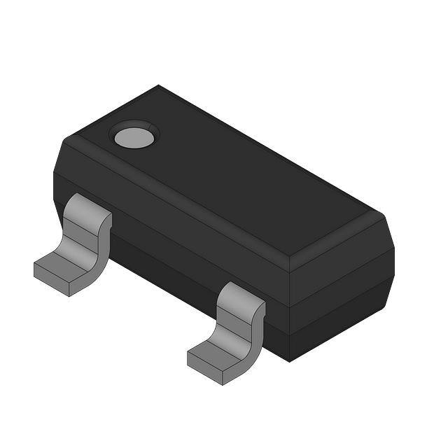
SOT−23
CASE 318
STYLE 6
PD
RqJA
MARKING DIAGRAM
PD
Maximum ratings are those values beyond which device damage can occur.
Maximum ratings applied to the device are individual stress limit values (not
normal operating conditions) and are not valid simultaneously. If these limits are
exceeded, device functional operation is not implied, damage may occur and
reliability may be affected.
1. FR−5 = 1.0 � 0.75 � 0.062 in.
2. Alumina = 0.4 � 0.3 � 0.024 in. 99.5% alumina.
2xx M G
G
1
2xx = Device Code
x = H for MMBTA55LT1
xx = GM for MMBTA56LT1
M = Date Code*
G
= Pb−Free Package
(Note: Microdot may be in either location)
*Date Code orientation and/or overbar may
vary depending upon manufacturing location.
ORDERING INFORMATION
See detailed ordering and shipping information in the package
dimensions section on page 4 of this data sheet.
Preferred devices are recommended choices for future use
and best overall value.
© Semiconductor Components Industries, LLC, 2006
January, 2006 − Rev. 4
1
Publication Order Number:
MMBTA55LT1/D
�MMBTA55LT1, MMBTA56LT1
ELECTRICAL CHARACTERISTICS (TA = 25°C unless otherwise noted)
Characteristic
Symbol
Min
Max
−60
−80
−
−
−4.0
−
−
−0.1
−
−
−0.1
−0.1
100
100
−
−
−
−0.25
−
−1.2
50
−
Unit
OFF CHARACTERISTICS
Collector −Emitter Breakdown Voltage (Note 3)
(IC = −1.0 mAdc, IB = 0)
V(BR)CEO
Vdc
MMBTA55
MMBTA56
Emitter −Base Breakdown Voltage
(IE = −100 mAdc, IC = 0)
V(BR)EBO
Collector Cutoff Current
(VCE = −60 Vdc, IB = 0)
Vdc
mAdc
ICES
Collector Cutoff Current
(VCB = −60 Vdc, IE = 0)
(VCB = −80 Vdc, IE = 0)
mAdc
ICBO
MMBTA55
MMBTA56
ON CHARACTERISTICS
DC Current Gain
(IC = −10 mAdc, VCE = −1.0 Vdc)
(IC = −100 mAdc, VCE = −1.0 Vdc)
hFE
Collector −Emitter Saturation Voltage
(IC = −100 mAdc, IB = −10 mAdc)
VCE(sat)
Base −Emitter On Voltage
(IC = −100 mAdc, VCE = −1.0 Vdc)
VBE(on)
−
Vdc
Vdc
SMALL− SIGNAL CHARACTERISTICS
Current −Gain − Bandwidth Product (Note 4)
(IC = −100 mAdc, VCE = −1.0 Vdc, f = 100 MHz)
fT
MHz
3. Pulse Test: Pulse Width v 300 ms, Duty Cycle v 2.0%.
4. fT is defined as the frequency at which |hfe| extrapolates to unity.
TURN−ON TIME
5.0 ms
+40 V
100
VCC
+VBB
+40 V
RL
100
RL
OUTPUT
+10 V
Vin
0
TURN−OFF TIME
VCC
−1.0 V
tr = 3.0 ns
OUTPUT
RB
* CS t 6.0 pF
5.0 mF
RB
Vin
* CS t 6.0 pF
5.0 mF
100
100
5.0 ms
tr = 3.0 ns
*Total Shunt Capacitance of Test Jig and Connectors For PNP Test Circuits, Reverse All Voltage Polarities
Figure 1. Switching Time Test Circuits
http://onsemi.com
2
�f T , CURRENT−GAIN − BANDWIDTH PRODUCT (MHz
MMBTA55LT1, MMBTA56LT1
200
100
VCE = −2.0 V
TJ = 25°C
TJ = 25°C
70
C, CAPACITANCE (pF)
50
100
70
50
30
Cibo
30
20
Cobo
10
7.0
20
−2.0 −3.0
−5.0 −7.0 −10
−20 −30 −50 −70 −100
IC, COLLECTOR CURRENT (mA)
5.0
−0.1 −0.2
−200
−0.5 −1.0 −2.0
−5.0 −10 −20
VR, REVERSE VOLTAGE (VOLTS)
Figure 2. Current−Gain — Bandwidth Product
1.0 k
700
500
TJ = 125°C
h FE, DC CURRENT GAIN
100
70
50
tf
VCC = −40 V
IC/IB = 10
IB1 = IB2
TJ = 25°C
10
−5.0 −7.0 −10
200
25°C
100
80
60
40
−0.5 −1.0 −2.0
−50 −70 −100
−200 −300 −500
−20 −30
IC, COLLECTOR CURRENT (mA)
Figure 4. Switching Time
−1.0
−55°C
tr
td @ VBE(off) = −0.5 V
−50 −100 −200
−5.0 −10 −20
IC, COLLECTOR CURRENT (mA)
Figure 5. DC Current Gain
TJ = 25°C
−0.8
V, VOLTAGE (VOLTS)
t, TIME (ns)
VCE = −1.0 V
ts
200
20
Figure 3. Capacitance
400
300
30
−50 −100
VBE(sat) @ IC/IB = 10
−0.6
VBE(on) @ VCE = −1.0 V
−0.4
−0.2
VCE(sat) @ IC/IB = 10
0
−0.5 −1.0 −2.0
−5.0 −10 −20
−50 −100 −200
IC, COLLECTOR CURRENT (mA)
Figure 6. “ON” Voltages
http://onsemi.com
3
−500
−500
�−1.0
R qVB , TEMPERATURE COEFFICIENT (mV/° C)
VCE , COLLECTOR−EMITTER VOLTAGE (VOLTS
MMBTA55LT1, MMBTA56LT1
TJ = 25°C
−0.8
IC =
−100 mA
IC =
−50 mA
IC =
−250 mA
IC =
−500 mA
−0.6
−0.4
−0.2
IC =
−10 mA
0
−0.05 −0.1 −0.2
−0.5
−1.0
−2.0
−5.0
−10
−20
−50
−0.8
−1.2
−1.6
RqVB for VBE
−2.0
−2.4
−2.8
−0.5 −1.0 −2.0
−5.0
−10
−20
−50
−100 −200
−500
IC, COLLECTOR CURRENT (mA)
IB, BASE CURRENT (mA)
Figure 8. Base−Emitter Temperature Coefficient
Figure 7. Collector Saturation Region
ORDERING INFORMATION
Device Order Number
Package Type
Shipping †
SOT−23
3,000 / Tape & Reel
SOT−23
(Pb−Free)
3,000 / Tape & Reel
SOT−23
10,000 / Tape & Reel
SOT−23
(Pb−Free)
10,000 / Tape & Reel
SOT−23
3,000 / Tape & Reel
SOT−23
(Pb−Free)
3,000 / Tape & Reel
SOT−23
10,000 / Tape & Reel
SOT−23
(Pb−Free)
10,000 / Tape & Reel
MMBTA55LT1
MMBTA55LT1G
MMBTA55LT3
MMBTA55LT3G
MMBTA56LT1
MMBTA56LT1G
MMBTA56LT3
MMBTA56LT3G
†For information on tape and reel specifications, including part orientation and tape sizes, please refer to our Tape and Reel Packaging
Specifications Brochure, BRD8011/D.
http://onsemi.com
4
�MMBTA55LT1, MMBTA56LT1
PACKAGE DIMENSIONS
SOT−23 (TO−236)
CASE 318−08
ISSUE AN
NOTES:
1. DIMENSIONING AND TOLERANCING PER ANSI
Y14.5M, 1982.
2. CONTROLLING DIMENSION: INCH.
3. MAXIMUM LEAD THICKNESS INCLUDES LEAD
FINISH THICKNESS. MINIMUM LEAD
THICKNESS IS THE MINIMUM THICKNESS OF
BASE MATERIAL.
4. 318−01 THRU −07 AND −09 OBSOLETE, NEW
STANDARD 318−08.
D
SEE VIEW C
3
HE
E
c
1
2
b
DIM
A
A1
b
c
D
E
e
L
L1
HE
0.25
e
q
A
L
A1
L1
MIN
0.89
0.01
0.37
0.09
2.80
1.20
1.78
0.10
0.35
2.10
MILLIMETERS
NOM
MAX
1.00
1.11
0.06
0.10
0.44
0.50
0.13
0.18
2.90
3.04
1.30
1.40
1.90
2.04
0.20
0.30
0.54
0.69
2.40
2.64
MIN
0.035
0.001
0.015
0.003
0.110
0.047
0.070
0.004
0.014
0.083
INCHES
NOM
0.040
0.002
0.018
0.005
0.114
0.051
0.075
0.008
0.021
0.094
MAX
0.044
0.004
0.020
0.007
0.120
0.055
0.081
0.012
0.029
0.104
STYLE 6:
PIN 1. BASE
2. EMITTER
3. COLLECTOR
VIEW C
SOLDERING FOOTPRINT*
0.95
0.037
0.95
0.037
2.0
0.079
0.9
0.035
SCALE 10:1
0.8
0.031
mm Ǔ
ǒinches
*For additional information on our Pb−Free strategy and soldering
details, please download the ON Semiconductor Soldering and
Mounting Techniques Reference Manual, SOLDERRM/D.
ON Semiconductor and
are registered trademarks of Semiconductor Components Industries, LLC (SCILLC). SCILLC reserves the right to make changes without further notice
to any products herein. SCILLC makes no warranty, representation or guarantee regarding the suitability of its products for any particular purpose, nor does SCILLC assume any liability
arising out of the application or use of any product or circuit, and specifically disclaims any and all liability, including without limitation special, consequential or incidental damages.
“Typical” parameters which may be provided in SCILLC data sheets and/or specifications can and do vary in different applications and actual performance may vary over time. All
operating parameters, including “Typicals” must be validated for each customer application by customer’s technical experts. SCILLC does not convey any license under its patent rights
nor the rights of others. SCILLC products are not designed, intended, or authorized for use as components in systems intended for surgical implant into the body, or other applications
intended to support or sustain life, or for any other application in which the failure of the SCILLC product could create a situation where personal injury or death may occur. Should
Buyer purchase or use SCILLC products for any such unintended or unauthorized application, Buyer shall indemnify and hold SCILLC and its officers, employees, subsidiaries, affiliates,
and distributors harmless against all claims, costs, damages, and expenses, and reasonable attorney fees arising out of, directly or indirectly, any claim of personal injury or death
associated with such unintended or unauthorized use, even if such claim alleges that SCILLC was negligent regarding the design or manufacture of the part. SCILLC is an Equal
Opportunity/Affirmative Action Employer. This literature is subject to all applicable copyright laws and is not for resale in any manner.
PUBLICATION ORDERING INFORMATION
LITERATURE FULFILLMENT:
N. American Technical Support: 800−282−9855 Toll Free
Literature Distribution Center for ON Semiconductor
USA/Canada
P.O. Box 61312, Phoenix, Arizona 85082−1312 USA
Phone: 480−829−7710 or 800−344−3860 Toll Free USA/Canada Japan: ON Semiconductor, Japan Customer Focus Center
2−9−1 Kamimeguro, Meguro−ku, Tokyo, Japan 153−0051
Fax: 480−829−7709 or 800−344−3867 Toll Free USA/Canada
Phone: 81−3−5773−3850
Email: orderlit@onsemi.com
http://onsemi.com
5
ON Semiconductor Website: http://onsemi.com
Order Literature: http://www.onsemi.com/litorder
For additional information, please contact your
local Sales Representative.
MMBTA55LT1/D
�


 工商网监
湘ICP备2023018690号
工商网监
湘ICP备2023018690号
