MOTOROLA
SEMICONDUCTOR TECHNICAL DATA
Amplifier Transistor
MPS6428
NPN Silicon
COLLECTOR
3
2
BASE
1
1
EMITTER
2
3
CASE 29–04, STYLE 1
TO–92 (TO–226AA)
MAXIMUM RATINGS
Rating
Symbol
Value
Unit
Collector – Emitter Voltage
VCEO
50
Vdc
Collector – Base Voltage
VCBO
60
Vdc
Emitter – Base Voltage
VEBO
6.0
Vdc
Collector Current — Continuous
IC
200
mAdc
Total Device Dissipation @ TA = 25°C
Derate above 25°C
PD
625
5.0
mW
mW/°C
Total Device Dissipation @ TC = 25°C
Derate above 25°C
PD
1.5
12
Watts
mW/°C
TJ, Tstg
– 55 to +150
°C
Operating and Storage Junction
Temperature Range
THERMAL CHARACTERISTICS
Symbol
Max
Unit
Thermal Resistance, Junction to Ambient
Characteristic
RqJA
200
°C/W
Thermal Resistance, Junction to Case
RqJC
83.3
°C/W
ELECTRICAL CHARACTERISTICS (TA = 25°C unless otherwise noted)
Characteristic
Symbol
Min
Max
Unit
Collector – Emitter Breakdown Voltage
(IC = 1.0 mAdc, IB = 0)
V(BR)CEO
50
—
Vdc
Collector – Base Breakdown Voltage
(IC = 0.1 mAdc, IE = 0)
V(BR)CBO
60
—
Vdc
Collector Cutoff Current
(VCE = 30 Vdc)
ICES
—
0.025
mA
Collector Cutoff Current
(VCB = 30 Vdc, IE = 0)
ICBO
—
0.01
mA
Emitter Cutoff Current
(VEB = 5.0 Vdc, IC = 0)
IEBO
—
0.01
mA
OFF CHARACTERISTICS
2–580
Motorola Small–Signal Transistors, FETs and Diodes Device Data
�MPS6428
ELECTRICAL CHARACTERISTICS (TA = 25°C unless otherwise noted) (Continued)
Characteristic
Symbol
Min
Max
250
250
250
250
—
650
—
—
—
—
0.2
0.6
Unit
ON CHARACTERISTICS
DC Current Gain
(VCE = 5.0 Vdc, IC = 0.01 mAdc)
(VCE = 5.0 Vdc, IC = 0.1 mAdc)
(VCE = 5.0 Vdc, IC = 1.0 mAdc)
(VCE = 5.0 Vdc, IC = 10 mAdc)
hFE
—
Collector – Emitter Saturation Voltage
(IC = 10 mAdc, IB = 0.5 mAdc)
(IC = 100 mAdc, IB = 5.0 mAdc)
VCE(sat)
Vdc
Base – Emitter On Voltage
(IC = 1.0 mAdc, VCE = 5.0 Vdc)
VBE(on)
0.56
0.66
Vdc
fT
100
700
MHz
Output Capacitance
(VCB = 10 Vdc, IE = 0, f = 1.0 MHz)
Cobo
—
3.0
pF
Input Capacitance
(VEB = 0.5 Vdc, IC = 0, f = 1.0 MHz)
Cibo
—
8.0
pF
Input Impedance
(IC = 1.0 mAdc, VCE = 5.0 Vdc, f = 1.0 kHz)
hie
3.0
30
kΩ
Voltage Feedback Ratio
(IC = 1.0 mAdc, VCE = 5.0 Vdc, f = 1.0 kHz)
hre
2.0
20
X 10– 4
Small–Signal Current Gain
(IC = 1.0 mAdc, VCE = 5.0 Vdc, f = 1.0 kHz)
hfe
200
800
—
Output Admittance
(IC = 1.0 mAdc, VCE = 5.0 Vdc, f = 1.0 kHz)
hoe
5.0
50
mmhos
SMALL– SIGNAL CHARACTERISTICS
Current – Gain — Bandwidth Product
(IC = 1.0 mAdc, VCE = 5.0 V, f = 100 MHz)
NOISE FIGURE/TOTAL NOISE VOLTAGE CHARACTERISTICS
Noise Figure/Voltage
(VCE = 5.0 V, IC = 0.1 mA, TA = 25°C)
NF
VT
Max (1)
NF
VT
Max (2)
NF
VT
Max (3)
7.0
6.0
3.5
18.1
5700
4.3
Unit
dB
nV
1. RS = 10 kΩ, BW = 1.0 Hz, f = 100 Hz
2. RS = 50 kΩ, BW = 15.7 kHz, f = 10 Hz–10 kHz
3. RS = 500 Ω, BW = 1.0 Hz, f = 10 Hz
Motorola Small–Signal Transistors, FETs and Diodes Device Data
2–581
�EMBOSSED TAPE AND REEL
SOT-23, SC-59, SC-70/SOT-323, SC–90/SOT–416, SOT-223 and SO-16 packages are available only in
Tape and Reel. Use the appropriate suffix indicated below to order any of the SOT-23, SC-59,
SC-70/SOT-323, SOT-223 and SO-16 packages. (See Section 6 on Packaging for additional information).
SOT-23:
available in 8 mm Tape and Reel
Use the device title (which already includes the “T1” suffix) to order the 7 inch/3000 unit reel.
Replace the “T1” suffix in the device title with a “T3” suffix to order the 13 inch/10,000 unit reel.
SC-59:
available in 8 mm Tape and Reel
Use the device title (which already includes the “T1” suffix) to order the 7 inch/3000 unit reel.
Replace the “T1” suffix in the device title with a “T3” suffix to order the 13 inch/10,000 unit reel.
SC-70/
SOT-323:
available in 8 mm Tape and Reel
Use the device title (which already includes the “T1” suffix) to order the 7 inch/3000 unit reel.
Replace the “T1” suffix in the device title with a “T3” suffix to order the 13 inch/10,000 unit reel.
SOT-223:
available in 12 mm Tape and Reel
Use the device title (which already includes the “T1” suffix) to order the 7 inch/1000 unit reel.
Replace the “T1” suffix in the device title with a “T3” suffix to order the 13 inch/4000 unit reel.
SO-16:
available in 16 mm Tape and Reel
Add an “R1” suffix to the device title to order the 7 inch/500 unit reel.
Add an “R2” suffix to the device title to order the 13 inch/2500 unit reel.
RADIAL TAPE IN FAN FOLD BOX OR REEL
TO-92 packages are available in both bulk shipments and in Radial Tape in Fan Fold Boxes or Reels.
Fan Fold Boxes and Radial Tape Reel are the best methods for capturing devices for automatic insertion in
printed circuit boards.
TO-92:
available in Fan Fold Box
Add an “RLR” suffix and the appropriate Style code* to the device title to order the Fan Fold box.
available in 365 mm Radial Tape Reel
Add an “RLR” suffix and the appropriate Style code* to the device title to order the Radial Tape
Reel.
*Refer to Section 6 on Packaging for Style code characters and additional information on ordering
*requirements.
DEVICE MARKINGS/DATE CODE CHARACTERS
SOT-23, SC-59, SC-70/SOT-323, and the SC–90/SOT–416 packages have a device marking and a date
code etched on the device. The generic example below depicts both the device marking and a representation of the date code that appears on the SC-70/SOT-323, SC-59 and SOT-23 packages.
ABC D
The “D” represents a smaller alpha digit Date Code. The Date Code indicates the actual month in which the
part was manufactured.
2–2
Motorola Small–Signal Transistors, FETs and Diodes Device Data
�Tape and Reel Specifications
and Packaging Specifications
Embossed Tape and Reel is used to facilitate automatic pick and place equipment feed requirements. The tape is used as the
shipping container for various products and requires a minimum of handling. The antistatic/conductive tape provides a secure
cavity for the product when sealed with the “peel–back” cover tape.
•
•
•
•
• SOD–123, SC–59, SC–70/SOT–323, SC–70ML/SOT–363,
SOT–23, TSOP–6, in 8 mm Tape
• SOT–223 in 12 mm Tape
• SO–14, SO–16 in 16 mm Tape
Two Reel Sizes Available (7″ and 13″)
Used for Automatic Pick and Place Feed Systems
Minimizes Product Handling
EIA 481, –1, –2
Use the standard device title and add the required suffix as listed in the option table on the following page. Note that the individual
reels have a finite number of devices depending on the type of product contained in the tape. Also note the minimum lot size is
one full reel for each line item, and orders are required to be in increments of the single reel quantity.
SOD–123
SC–59, SC–70/SOT–323, SOT–23
8 mm
8 mm
SOT–223
SC–70ML/SOT–363, TSOP–6
T1 ORIENTATION
8 mm
SO–14, 16
12 mm
16 mm
SC–70ML/SOT–363
T2 ORIENTATION
DIRECTION
8 mm
OF FEED
EMBOSSED TAPE AND REEL ORDERING INFORMATION
Devices Per Reel
and Minimum
Order Quantity
Device
Suffix
(7)
3,000
T1
178
330
(7)
(13)
3,000
10,000
T1
T3
8.0 ± 0.1 (.315 ± .004)
178
330
(7)
(13)
500
2,500
R1
R2
16
16
8.0 ± 0.1 (.315 ± .004)
178
330
(7)
(13)
500
2,500
R1
R2
SOD–123
8
8
4.0 ± 0.1 (.157 ± .004)
178
330
(7)
(13)
3,000
10,000
T1
T3
SOT–23
8
8
4.0 ± 0.1 (.157 ± .004)
178
330
(7)
(13)
3,000
10,000
T1
T3
SOT–223
12
12
8.0 ± 0.1 (.315 ± .004)
178
330
(7)
(13)
1,000
4,000
T1
T3
SC–70ML/SOT–363
8
8
4.0 ± 0.1 (.157 ± .004)
178
178
(7)
(7)
3,000
3,000
T1
T2
TSOP–6
8
4.0 ± 0.1 (.157 ± .004)
178
(7)
3,000
T1
Package
Tape Width
(mm)
Pitch
mm
(inch)
SC–59
8
4.0 ± 0.1 (.157 ± .004)
178
SC–70/SOT–323
8
8
4.0 ± 0.1 (.157 ± .004)
SO–14
16
16
SO–16
Tape and Reel Specifications
6–2
Reel Size
mm
(inch)
Motorola Small–Signal Transistors, FETs and Diodes Device Data
�EMBOSSED TAPE AND REEL DATA FOR DISCRETES
CARRIER TAPE SPECIFICATIONS
P0
K
P2
D
t
10 Pitches Cumulative Tolerance on Tape
± 0.2 mm
(± 0.008″)
E
Top Cover
Tape
A0
K0
B1
F
W
B0
See
Note 1
P
For Machine Reference Only
Including Draft and RADII
Concentric Around B0
D1
For Components
2.0 mm x 1.2 mm and Larger
Center Lines
of Cavity
Embossment
User Direction of Feed
* Top Cover Tape
Thickness (t1)
0.10 mm
(.004″) Max.
Bar Code Label
R Min
Tape and Components
Shall Pass Around Radius “R”
Without Damage
Bending Radius
10°
Embossed Carrier
100 mm
(3.937″)
Maximum Component Rotation
Embossment
1 mm Max
Typical Component
Cavity Center Line
Tape
1 mm
(.039″) Max
Typical Component
Center Line
250 mm
(9.843″)
Camber (Top View)
Allowable Camber To Be 1 mm/100 mm Nonaccumulative Over 250 mm
DIMENSIONS
Tape
Size
B1 Max
D
D1
E
F
K
P0
P2
R Min
T Max
W Max
8 mm
4.55 mm
(.179″)
1.0 Min
(.039″)
1.75 ± 0.1 mm
(.069 ± .004″)
3.5 ± 0.05 mm
(.138 ± .002″)
2.4 mm Max
(.094″)
4.0 ± 0.1 mm
(.157 ± .004″)
2.0 ± 0.1 mm
(.079 ± .002″)
25 mm
(.98″)
0.6 mm
(.024″)
8.3 mm
(.327″)
12 mm
8.2 mm
(.323″)
1.5 + 0.1 mm
– 0.0
( 0 9 + .004″
004
(.059
– 0.0)
5.5 ± 0.05 mm
(.217 ± .002″)
6.4 mm Max
(.252″)
16 mm
12.1 mm
(.476″)
7.5 ± 0.10 mm
(.295 ± .004″)
7.9 mm Max
(.311″)
16.3 mm
(.642″)
24 mm
20.1 mm
(.791″)
11.5 ± 0.1 mm
(.453 ± .004″)
11.9 mm Max
(.468″)
24.3 mm
(.957″)
1.5 mm Min
(.060″)
30 mm
(1.18″)
12 ± .30 mm
(.470 ± .012″)
Metric dimensions govern — English are in parentheses for reference only.
NOTE 1: A0, B0, and K0 are determined by component size. The clearance between the components and the cavity must be within .05 mm min. to .50 mm max.,
NOTE 1: the component cannot rotate more than 10° within the determined cavity.
NOTE 2: If B1 exceeds 4.2 mm (.165) for 8 mm embossed tape, the tape may not feed through all tape feeders.
NOTE 3: Pitch information is contained in the Embossed Tape and Reel Ordering Information on pg. 5.12–3.
Motorola Small–Signal Transistors, FETs and Diodes Device Data
Tape and Reel Specifications
6–3
�EMBOSSED TAPE AND REEL DATA FOR DISCRETES
T Max
Outside Dimension
Measured at Edge
1.5 mm Min
(.06″)
A
13.0 mm ± 0.5 mm
(.512″ ± .002″)
20.2 mm Min
(.795″)
50 mm Min
(1.969″)
Full Radius
G
Size
A Max
8 mm
330 mm
(12.992″)
8.4 mm + 1.5 mm, – 0.0
(.33″ + .059″, – 0.00)
14.4 mm
(.56″)
12 mm
330 mm
(12.992″)
12.4 mm + 2.0 mm, – 0.0
(.49″ + .079″, – 0.00)
18.4 mm
(.72″)
16 mm
360 mm
(14.173″)
16.4 mm + 2.0 mm, – 0.0
(.646″ + .078″, – 0.00)
22.4 mm
(.882″)
24 mm
360 mm
(14.173″)
24.4 mm + 2.0 mm, – 0.0
(.961″ + .070″, – 0.00)
30.4 mm
(1.197″)
G
Inside Dimension
Measured Near Hub
T Max
Reel Dimensions
Metric Dimensions Govern — English are in parentheses for reference only
Tape and Reel Specifications
6–4
Motorola Small–Signal Transistors, FETs and Diodes Device Data
�TO–92 EIA, IEC, EIAJ
Radial Tape in Fan Fold
Box or On Reel
TO–92
RADIAL
TAPE IN
FAN FOLD
BOX OR
ON REEL
Radial tape in fan fold box or on reel of the reliable TO–92 package are
the best methods of capturing devices for automatic insertion in printed
circuit boards. These methods of taping are compatible with various
equipment for active and passive component insertion.
•
•
•
•
•
•
Available in Fan Fold Box
Available on 365 mm Reels
Accommodates All Standard Inserters
Allows Flexible Circuit Board Layout
2.5 mm Pin Spacing for Soldering
EIA–468, IEC 286–2, EIAJ RC1008B
Ordering Notes:
When ordering radial tape in fan fold box or on reel, specify the style per
Figures 3 through 8. Add the suffix “RLR” and “Style” to the device title, i.e.
MPS3904RLRA. This will be a standard MPS3904 radial taped and
supplied on a reel per Figure 9.
Fan Fold Box Information — Order in increments of 2000.
Reel Information — Order in increments of 2000.
US/European Suffix Conversions
US
EUROPE
RLRA
RL
RLRE
RL1
RLRM
ZL1
Motorola Small–Signal Transistors, FETs and Diodes Device Data
Packaging Specifications
6–5
�TO–92 EIA RADIAL TAPE IN FAN FOLD BOX OR ON REEL
H2A
H2A
H2B
H2B
H
W2
H4 H5
T1
L1
H1
W1 W
L
T
T2
F1
F2
P2
P2
P1
D
P
Figure 1. Device Positioning on Tape
Specification
Inches
Symbol
Item
Millimeter
Min
Max
Min
Max
D
Tape Feedhole Diameter
0.1496
0.1653
3.8
4.2
D2
Component Lead Thickness Dimension
0.015
0.020
0.38
0.51
Component Lead Pitch
0.0945
0.110
2.4
2.8
.059
.156
1.5
4.0
0.3346
0.3741
8.5
9.5
Deflection Left or Right
0
0.039
0
1.0
Deflection Front or Rear
0
0.051
0
1.0
Feedhole to Bottom of Component
0.7086
0.768
18
19.5
Feedhole to Seating Plane
0.610
0.649
15.5
16.5
F1, F2
H
H1
H2A
H2B
H4
H5
L
Bottom of Component to Seating Plane
Feedhole Location
Defective Unit Clipped Dimension
0.3346
0.433
8.5
11
L1
Lead Wire Enclosure
0.09842
—
2.5
—
P
Feedhole Pitch
0.4921
0.5079
12.5
12.9
P1
Feedhole Center to Center Lead
0.2342
0.2658
5.95
6.75
P2
First Lead Spacing Dimension
0.1397
0.1556
3.55
3.95
0.06
0.08
0.15
0.20
T
Adhesive Tape Thickness
T1
Overall Taped Package Thickness
—
0.0567
—
1.44
T2
Carrier Strip Thickness
0.014
0.027
0.35
0.65
W
Carrier Strip Width
0.6889
0.7481
17.5
19
W1
Adhesive Tape Width
0.2165
0.2841
5.5
6.3
W2
Adhesive Tape Position
.0059
0.01968
.15
0.5
NOTES:
1. Maximum alignment deviation between leads not to be greater than 0.2 mm.
2. Defective components shall be clipped from the carrier tape such that the remaining protrusion (L) does not exceed a maximum of 11 mm.
3. Component lead to tape adhesion must meet the pull test requirements established in Figures 5, 6 and 7.
4. Maximum non–cumulative variation between tape feed holes shall not exceed 1 mm in 20 pitches.
5. Holddown tape not to extend beyond the edge(s) of carrier tape and there shall be no exposure of adhesive.
6. No more than 1 consecutive missing component is permitted.
7. A tape trailer and leader, having at least three feed holes is required before the first and after the last component.
8. Splices will not interfere with the sprocket feed holes.
Packaging Specifications
6–6
Motorola Small–Signal Transistors, FETs and Diodes Device Data
�TO–92 EIA RADIAL TAPE IN FAN FOLD BOX OR ON REEL
FAN FOLD BOX STYLES
ÇÇÇÇÇÇÇ
ÇÇÇÇÇÇÇ
ÇÇÇÇÇÇÇ
ÇÇÇÇÇÇÇ
ADHESIVE TAPE ON
TOP SIDE
FLAT SIDE
ADHESIVE TAPE ON
TOP SIDE
ROUNDED SIDE
CARRIER
STRIP
CARRIER
STRIP
Figure 2. Style M
252 mm
9.92”
FLAT SIDE OF TRANSISTOR
AND ADHESIVE TAPE VISIBLE.
Style M fan fold box is equivalent to styles E and F of
reel pack dependent on feed orientation from box.
330 mm
13”
MAX
ROUNDED SIDE OF TRANSISTOR AND
ADHESIVE TAPE VISIBLE.
Style P fan fold box is equivalent to styles A and B of
reel pack dependent on feed orientation from box.
Figure 3. Style P
MAX
58 mm
2.28”
MAX
Figure 4. Fan Fold Box Dimensions
ADHESION PULL TESTS
500 GRAM PULL FORCE
70 GRAM
PULL FORCE
100 GRAM
PULL FORCE
16 mm
16 mm
HOLDING
FIXTURE
The component shall not pull free with a 300 gram
load applied to the leads for 3 ± 1 second.
Figure 5. Test #1
HOLDING
FIXTURE
The component shall not pull free with a 70 gram
load applied to the leads for 3 ± 1 second.
Figure 6. Test #2
Motorola Small–Signal Transistors, FETs and Diodes Device Data
HOLDING
FIXTURE
There shall be no deviation in the leads and
no component leads shall be pulled free of
the tape with a 500 gram load applied to the
component body for 3 ± 1 second.
Figure 7. Test #3
Packaging Specifications
6–7
�TO–92 EIA RADIAL TAPE IN FAN FOLD BOX OR ON REEL
REEL STYLES
CORE DIA.
82mm ± 1mm
ARBOR HOLE DIA.
30.5mm ± 0.25mm
MARKING NOTE
HUB RECESS
76.2mm ± 1mm
RECESS DEPTH
9.5mm MIN
365mm + 3, – 0mm
38.1mm ± 1mm
48 mm
MAX
Material used must not cause deterioration of components or degrade lead solderability
Figure 8. Reel Specifications
ADHESIVE TAPE ON REVERSE SIDE
CARRIER STRIP
CARRIER STRIP
ROUNDED
SIDE
FLAT SIDE
ADHESIVE TAPE
FEED
FEED
Rounded side of transistor and adhesive tape visible.
Flat side of transistor and carrier strip visible
(adhesive tape on reverse side).
Figure 9. Style A
Figure 10. Style B
ADHESIVE TAPE ON REVERSE SIDE
CARRIER STRIP
CARRIER STRIP
FLAT SIDE
ROUNDED
SIDE
ADHESIVE TAPE
FEED
FEED
Flat side of transistor and adhesive tape visible.
Figure 11. Style E
Packaging Specifications
6–8
Rounded side of transistor and carrier strip visible
(adhesive tape on reverse side).
Figure 12. Style F
Motorola Small–Signal Transistors, FETs and Diodes Device Data
�INFORMATION FOR USING SURFACE MOUNT PACKAGES
RECOMMENDED FOOTPRINTS FOR SURFACE MOUNTED APPLICATIONS
Surface mount board layout is a critical portion of the total
design. The footprint for the semiconductor packages must
be the correct size to ensure proper solder connection inter-
face between the board and the package. With the correct
pad geometry, the packages will self align when subjected to
a solder reflow process.
POWER DISSIPATION FOR A SURFACE MOUNT DEVICE
PD =
TJ(max) – TA
RθJA
The values for the equation are found in the maximum
ratings table on the data sheet. Substituting these values into
the equation for an ambient temperature TA of 25°C, one can
calculate the power dissipation of the device. For example,
for a SOT–223 device, PD is calculated as follows.
PD = 150°C – 25°C = 800 milliwatts
156°C/W
The 156°C/W for the SOT–223 package assumes the use
of the recommended footprint on a glass epoxy printed circuit
board to achieve a power dissipation of 800 milliwatts. There
are other alternatives to achieving higher power dissipation
from the surface mount packages. One is to increase the
area of the drain/collector pad. By increasing the area of the
drain/collector pad, the power dissipation can be increased.
Although the power dissipation can almost be doubled with
this method, area is taken up on the printed circuit board
which can defeat the purpose of using surface mount
technology. For example, a graph of RθJA versus drain pad
area is shown in Figure 1.
Another alternative would be to use a ceramic substrate or
an aluminum core board such as Thermal Clad. Using a
board material such as Thermal Clad, an aluminum core
board, the power dissipation can be doubled using the same
footprint.
RθJA , THERMAL RESISTANCE, JUNCTION
TO AMBIENT (°C/W)
The power dissipation for a surface mount device is a function of the drain/collector pad size. These can vary from the
minimum pad size for soldering to a pad size given for
maximum power dissipation. Power dissipation for a surface
mount device is determined by TJ(max), the maximum rated
junction temperature of the die, RθJA, the thermal resistance
from the device junction to ambient, and the operating
temperature, TA. Using the values provided on the data
sheet, PD can be calculated as follows:
160
140
Board Material = 0.0625″
G–10/FR–4, 2 oz Copper
TA = 25°C
0.8 Watts
120
1.25 Watts*
1.5 Watts
100
80
0.0
*Mounted on the DPAK footprint
0.2
0.4
0.6
A, AREA (SQUARE INCHES)
0.8
1.0
Figure 1. Thermal Resistance versus Drain Pad
Area for the SOT–223 Package (Typical)
SOLDER STENCIL GUIDELINES
Prior to placing surface mount components onto a printed
circuit board, solder paste must be applied to the pads.
Solder stencils are used to screen the optimum amount.
These stencils are typically 0.008 inches thick and may be
made of brass or stainless steel. For packages such as the
Surface Mount Information
7–10
SOT–23, SC–59, SC–70/SOT–323, SC–90/SOT–416,
SOD–123, SOT–223, SOT–363, SO–14, SO–16, and
TSOP–6 packages, the stencil opening should be the same
as the pad size or a 1:1 registration.
Motorola Small–Signal Transistors, FETs and Diodes Device Data
�SOLDERING PRECAUTIONS
The melting temperature of solder is higher than the rated
temperature of the device. When the entire device is heated
to a high temperature, failure to complete soldering within a
short time could result in device failure. Therefore, the
following items should always be observed in order to minimize the thermal stress to which the devices are subjected.
• Always preheat the device.
• The delta temperature between the preheat and soldering
should be 100°C or less.*
• When preheating and soldering, the temperature of the
leads and the case must not exceed the maximum
temperature ratings as shown on the data sheet. When
using infrared heating with the reflow soldering method,
the difference should be a maximum of 10°C.
• The soldering temperature and time should not exceed
260°C for more than 10 seconds.
• When shifting from preheating to soldering, the maximum
temperature gradient shall be 5°C or less.
• After soldering has been completed, the device should be
allowed to cool naturally for at least three minutes.
Gradual cooling should be used since the use of forced
cooling will increase the temperature gradient and will
result in latent failure due to mechanical stress.
• Mechanical stress or shock should not be applied during
cooling.
* Soldering a device without preheating can cause excessive
thermal shock and stress which can result in damage to the
device.
TYPICAL SOLDER HEATING PROFILE
For any given circuit board, there will be a group of control
settings that will give the desired heat pattern. The operator
must set temperatures for several heating zones and a figure
for belt speed. Taken together, these control settings make
up a heating “profile” for that particular circuit board. On
machines controlled by a computer, the computer remembers these profiles from one operating session to the next.
Figure 2 shows a typical heating profile for use when
soldering a surface mount device to a printed circuit board.
This profile will vary among soldering systems, but it is a
good starting point. Factors that can affect the profile include
the type of soldering system in use, density and types of
components on the board, type of solder used, and the type
of board or substrate material being used. This profile shows
temperature versus time. The line on the graph shows the
STEP 1
PREHEAT
ZONE 1
“RAMP”
200°C
STEP 2 STEP 3
VENT
HEATING
“SOAK” ZONES 2 & 5
“RAMP”
DESIRED CURVE FOR HIGH
MASS ASSEMBLIES
actual temperature that might be experienced on the surface
of a test board at or near a central solder joint. The two
profiles are based on a high density and a low density board.
The Vitronics SMD310 convection/infrared reflow soldering
system was used to generate this profile. The type of solder
used was 62/36/2 Tin Lead Silver with a melting point
between 177 –189°C. When this type of furnace is used for
solder reflow work, the circuit boards and solder joints tend to
heat first. The components on the board are then heated by
conduction. The circuit board, because it has a large surface
area, absorbs the thermal energy more efficiently, then
distributes this energy to the components. Because of this
effect, the main body of a component may be up to 30
degrees cooler than the adjacent solder joints.
STEP 4
HEATING
ZONES 3 & 6
“SOAK”
STEP 5
HEATING
ZONES 4 & 7
“SPIKE”
STEP 6
VENT
STEP 7
COOLING
205° TO 219°C
PEAK AT
SOLDER JOINT
170°C
160°C
150°C
150°C
100°C
140°C
100°C
SOLDER IS LIQUID FOR
40 TO 80 SECONDS
(DEPENDING ON
MASS OF ASSEMBLY)
DESIRED CURVE FOR LOW
MASS ASSEMBLIES
50°C
TIME (3 TO 7 MINUTES TOTAL)
TMAX
Figure 2. Typical Solder Heating Profile
Motorola Small–Signal Transistors, FETs and Diodes Device Data
Surface Mount Information
7–11
�Footprints for Soldering
0.037
0.95
0.037
0.95
0.037
0.95
0.037
0.95
0.094
2.4
0.079
2.0
0.039
1.0
0.035
0.9
inches
0.031
0.8
0.031
0.8
mm
mm
SOT–23
0.025
0.025
0.65
0.65
ÉÉÉ
ÉÉÉ
ÉÉÉ
0.075
0.5 min. (3x)
1.9
0.035
0.9
0.028
1.4
inches
0.7
ÉÉÉ
ÉÉÉ
ÉÉÉ
ÉÉÉ
ÉÉÉ
ÉÉÉ
0.5
0.5 min. (3x)
1
SC–59
inches
mm
SC–70/SOT–323
SOT 416/SC–90
0.15
3.8
0.060
1.52
0.079
2.0
0.091
2.3
0.248
6.3
0.091
2.3
0.079
2.0
0.275
7.0
0.155
4.0
0.024
0.6
0.059
1.5
0.059
1.5
0.059
1.5
0.050
1.270
inches
inches
mm
mm
SOT–223
Surface Mount Information
7–12
SO–14, SO–16
Motorola Small–Signal Transistors, FETs and Diodes Device Data
�ÉÉÉ
ÉÉÉ
ÉÉÉ
ÉÉÉ
2.36
0.093
4.19
0.165
1.22
0.048
0.4 mm (min)
ÉÉÉÉ
ÉÉÉÉ
ÉÉÉÉ
ÉÉÉÉ
0.91
0.036
mm
inches
ÉÉÉ
ÉÉÉ
ÉÉÉ
ÉÉÉ
ÉÉÉ
ÉÉÉ
ÉÉÉ
ÉÉÉ
ÉÉÉ
ÉÉÉ
ÉÉÉ
ÉÉÉ
ÉÉÉ
ÉÉÉ
0.65 mm 0.65 mm
0.5 mm (min)
1.9 mm
SOD–123
SOT–363
(SC–70 6 LEAD)
0.094
2.4
0.037
0.95
0.074
1.9
0.037
0.95
0.028
0.7
0.039
1.0
inches
mm
TSOP–6
Motorola Small–Signal Transistors, FETs and Diodes Device Data
Surface Mount Information
7–13
�Package Outline Dimensions
Dimensions are in inches unless otherwise noted.
A
NOTES:
1. DIMENSIONING AND TOLERANCING PER ANSI
Y14.5M, 1982.
2. CONTROLLING DIMENSION: INCH.
3. CONTOUR OF PACKAGE BEYOND DIMENSION R
IS UNCONTROLLED.
4. DIMENSION F APPLIES BETWEEN P AND L.
DIMENSION D AND J APPLY BETWEEN L AND K
MINIMUM. LEAD DIMENSION IS UNCONTROLLED
IN P AND BEYOND DIMENSION K MINIMUM.
B
R
P
L
F
SEATING
PLANE
K
DIM
A
B
C
D
F
G
H
J
K
L
N
P
R
V
D
X X
G
J
H
V
C
SECTION X–X
1
N
N
STYLE 1:
PIN 1. EMITTER
2. BASE
3. COLLECTOR
STYLE 14:
PIN 1. EMITTER
2. COLLECTOR
3. BASE
STYLE 2:
PIN 1. BASE
2. EMITTER
3. COLLECTOR
STYLE 15:
PIN 1. ANODE 1
2. CATHODE
3. ANODE 2
STYLE 3:
PIN 1. ANODE
2. ANODE
3. CATHODE
STYLE 4:
PIN 1. CATHODE
2. CATHODE
3. ANODE
STYLE 17:
PIN 1. COLLECTOR
2. BASE
3. EMITTER
STYLE 21:
PIN 1. COLLECTOR
2. EMITTER
3. BASE
STYLE 5:
PIN 1. DRAIN
2. SOURCE
3. GATE
STYLE 22:
PIN 1. SOURCE
2. GATE
3. DRAIN
INCHES
MIN
MAX
0.175
0.205
0.170
0.210
0.125
0.165
0.016
0.022
0.016
0.019
0.045
0.055
0.095
0.105
0.015
0.020
0.500
–––
0.250
–––
0.080
0.105
–––
0.100
0.115
–––
0.135
–––
MILLIMETERS
MIN
MAX
4.45
5.20
4.32
5.33
3.18
4.19
0.41
0.55
0.41
0.48
1.15
1.39
2.42
2.66
0.39
0.50
12.70
–––
6.35
–––
2.04
2.66
–––
2.54
2.93
–––
3.43
–––
STYLE 7:
PIN 1. SOURCE
2. DRAIN
3. GATE
STYLE 30:
PIN 1. DRAIN
2. GATE
3. SOURCE
CASE 029–04
(TO–226AA) TO–92
PLASTIC
A
NOTES:
1. DIMENSIONING AND TOLERANCING PER ANSI
Y14.5M, 1982.
2. CONTROLLING DIMENSION: INCH.
3. CONTOUR OF PACKAGE BEYOND DIMENSION R
IS UNCONTROLLED.
4. DIMENSION F APPLIES BETWEEN P AND L.
DIMENSIONS D AND J APPLY BETWEEN L AND K
MIMIMUM. LEAD DIMENSION IS UNCONTROLLED
IN P AND BEYOND DIMENSION K MINIMUM.
B
R
SEATING
PLANE
P
L
F
K
X X
DIM
A
B
C
D
F
G
H
J
K
L
N
P
R
V
D
G
H
J
V
1 2 3
N C
SECTION X–X
N
STYLE 1:
PIN 1. EMITTER
2. BASE
3. COLLECTOR
STYLE 14:
PIN 1. EMITTER
2. COLLECTOR
3. BASE
INCHES
MIN
MAX
0.175
0.205
0.290
0.310
0.125
0.165
0.018
0.022
0.016
0.019
0.045
0.055
0.095
0.105
0.018
0.024
0.500
–––
0.250
–––
0.080
0.105
–––
0.100
0.135
–––
0.135
–––
MILLIMETERS
MIN
MAX
4.44
5.21
7.37
7.87
3.18
4.19
0.46
0.56
0.41
0.48
1.15
1.39
2.42
2.66
0.46
0.61
12.70
–––
6.35
–––
2.04
2.66
–––
2.54
3.43
–––
3.43
–––
STYLE 22:
PIN 1. SOURCE
2. GATE
3. DRAIN
CASE 029–05
(TO–226AE) TO–92
1–WATT PLASTIC
Package Outline Dimensions
8–2
Motorola Small–Signal Transistors, FETs and Diodes Device Data
�PACKAGE OUTLINE DIMENSIONS (continued)
B
NOTES:
1. PACKAGE CONTOUR OPTIONAL WITHIN DIA B
AND LENGTH A. HEAT SLUGS, IF ANY, SHALL BE
INCLUDED WITHIN THIS CYLINDER, BUT SHALL
NOT BE SUBJECT TO THE MIN LIMIT OF DIA B.
2. LEAD DIA NOT CONTROLLED IN ZONES F, TO
ALLOW FOR FLASH, LEAD FINISH BUILDUP,
AND MINOR IRREGULARITIES OTHER THAN
HEAT SLUGS.
D
K
F
A
DIM
A
B
D
F
K
F
K
MILLIMETERS
MIN
MAX
5.84
7.62
2.16
2.72
0.46
0.56
–––
1.27
25.40
38.10
INCHES
MIN
MAX
0.230
0.300
0.085
0.107
0.018
0.022
–––
0.050
1.000
1.500
All JEDEC dimensions and notes apply.
CASE 51–02
(DO–204AA)
DO–7
A
B
R
SEATING
PLANE
ÉÉ
ÉÉ
D
P
L
F
K
J
SECTION X–X
X X
D
G
H
V
1
2
C
N
N
NOTES:
1. DIMENSIONING AND TOLERANCING PER ANSI
Y14.5M, 1982.
2. CONTROLLING DIMENSION: INCH.
3. CONTOUR OF PACKAGE BEYOND ZONE R IS
UNCONTROLLED.
4. DIMENSION F APPLIES BETWEEN P AND L.
DIMENSIONS D AND J APPLY BETWEEN L AND K
MINIMUM. LEAD DIMENSION IS UNCONTROLLED
IN P AND BEYOND DIM K MINIMUM.
DIM
A
B
C
D
F
G
H
J
K
L
N
P
R
V
INCHES
MIN
MAX
0.175
0.205
0.170
0.210
0.125
0.165
0.016
0.022
0.016
0.019
0.050 BSC
0.100 BSC
0.014
0.016
0.500
–––
0.250
–––
0.080
0.105
–––
0.050
0.115
–––
0.135
–––
MILLIMETERS
MIN
MAX
4.45
5.21
4.32
5.33
3.18
4.49
0.41
0.56
0.407
0.482
1.27 BSC
3.54 BSC
0.36
0.41
12.70
–––
6.35
–––
2.03
2.66
–––
1.27
2.93
–––
3.43
–––
STYLE 1:
PIN 1. ANODE
2. CATHODE
CASE 182–02
(T0–226AC) TO–92
PLASTIC
Motorola Small–Signal Transistors, FETs and Diodes Device Data
Package Outline Dimensions
8–3
�PACKAGE OUTLINE DIMENSIONS (continued)
NOTES:
1. DIMENSIONING AND TOLERANCING PER ANSI
Y14.5M, 1982.
2. CONTROLLING DIMENSION: INCH.
3. MAXIUMUM LEAD THICKNESS INCLUDES
LEAD FINISH THICKNESS. MINIMUM LEAD
THICKNESS IS THE MINIMUM THICKNESS OF
BASE MATERIAL.
A
L
3
B S
1
DIM
A
B
C
D
G
H
J
K
L
S
V
2
V
G
C
H
D
STYLE 6:
PIN 1. BASE
2. EMITTER
3. COLLECTOR
STYLE 8:
PIN 1. ANODE
2. NO CONNECTION
3. CATHODE
STYLE 12:
PIN 1. CATHODE
2. CATHODE
3. ANODE
J
K
STYLE 10:
PIN 1. DRAIN
2. SOURCE
3. GATE
STYLE 9:
PIN 1. ANODE
2. ANODE
3. CATHODE
STYLE 18:
PIN 1. NO CONNECTION
2. CATHODE
3. ANODE
INCHES
MIN
MAX
0.1102 0.1197
0.0472 0.0551
0.0350 0.0440
0.0150 0.0200
0.0701 0.0807
0.0005 0.0040
0.0034 0.0070
0.0140 0.0285
0.0350 0.0401
0.0830 0.1039
0.0177 0.0236
STYLE 19:
PIN 1. CATHODE
2. ANODE
3. CATHODE–ANODE
MILLIMETERS
MIN
MAX
2.80
3.04
1.20
1.40
0.89
1.11
0.37
0.50
1.78
2.04
0.013
0.100
0.085
0.177
0.35
0.69
0.89
1.02
2.10
2.64
0.45
0.60
STYLE 11:
PIN 1. ANODE
2. CATHODE
3. CATHODE–ANODE
STYLE 21:
PIN 1. GATE
2. SOURCE
3. DRAIN
CASE 318–08
(TO–236AB) SOT–23
PLASTIC
A
NOTES:
1. DIMENSIONING AND TOLERANCING PER ANSI
Y14.5M, 1982.
2. CONTROLLING DIMENSION: MILLIMETER.
L
3
S
2
DIM
A
B
C
D
G
H
J
K
L
S
B
1
D
G
J
C
H
STYLE 1:
PIN 1. EMITTER
2. BASE
3. COLLECTOR
MILLIMETERS
MIN
MAX
2.70
3.10
1.30
1.70
1.00
1.30
0.35
0.50
1.70
2.10
0.013
0.100
0.09
0.18
0.20
0.60
1.25
1.65
2.50
3.00
INCHES
MIN
MAX
0.1063 0.1220
0.0512 0.0669
0.0394 0.0511
0.0138 0.0196
0.0670 0.0826
0.0005 0.0040
0.0034 0.0070
0.0079 0.0236
0.0493 0.0649
0.0985 0.1181
K
STYLE 2:
PIN 1. N.C.
2. ANODE
3. CATHODE
STYLE 3:
PIN 1. ANODE
2. ANODE
3. CATHODE
STYLE 4:
PIN 1. N.C.
2. CATHODE
3. ANODE
STYLE 5:
PIN 1. CATHODE
2. CATHODE
3. ANODE
CASE 318D–04
SC–59
Package Outline Dimensions
8–4
Motorola Small–Signal Transistors, FETs and Diodes Device Data
�PACKAGE OUTLINE DIMENSIONS (continued)
A
F
NOTES:
3. DIMENSIONING AND TOLERANCING PER ANSI
Y14.5M, 1982.
4. CONTROLLING DIMENSION: INCH.
4
S
INCHES
DIM MIN
MAX
A
0.249
0.263
B
0.130
0.145
C
0.060
0.068
D
0.024
0.035
F
0.115
0.126
G
0.087
0.094
H 0.0008 0.0040
J
0.009
0.014
K
0.060
0.078
L
0.033
0.041
M
0_
10 _
S
0.264
0.287
B
1
2
3
D
L
G
J
C
0.08 (0003)
M
H
MILLIMETERS
MIN
MAX
6.30
6.70
3.30
3.70
1.50
1.75
0.60
0.89
2.90
3.20
2.20
2.40
0.020
0.100
0.24
0.35
1.50
2.00
0.85
1.05
0_
10 _
6.70
7.30
K
STYLE 1:
PIN 1.
2.
3.
4.
BASE
COLLECTOR
EMITTER
COLLECTOR
STYLE 2:
PIN 1.
2.
3.
4.
ANODE
CATHODE
NC
CATHODE
STYLE 3:
PIN 1.
2.
3.
4.
GATE
DRAIN
SOURCE
DRAIN
CASE 318E–04
SOT–223
A
NOTES:
1. DIMENSIONING AND TOLERANCING PER ANSI
Y14.5M, 1982.
2. CONTROLLING DIMENSION: MILLIMETER.
3. MAXIMUM LEAD THICKNESS INCLUDES LEAD
FINISH THICKNESS. MINIMUM LEAD THICKNESS
IS THE MINIMUM THICKNESS OF BASE
MATERIAL.
L
6
5
4
2
3
B
S
1
D
G
M
J
C
0.05 (0.002)
H
K
DIM
A
B
C
D
G
H
J
K
L
M
S
MILLIMETERS
MIN
MAX
2.90
3.10
1.30
1.70
0.90
1.10
0.25
0.50
0.85
1.05
0.013
0.100
0.10
0.26
0.20
0.60
1.25
1.55
0_
10 _
2.50
3.00
STYLE 1:
PIN 1.
2.
3.
4.
5.
6.
INCHES
MIN
MAX
0.1142 0.1220
0.0512 0.0669
0.0354 0.0433
0.0098 0.0197
0.0335 0.0413
0.0005 0.0040
0.0040 0.0102
0.0079 0.0236
0.0493 0.0610
0_
10 _
0.0985 0.1181
DRAIN
DRAIN
GATE
SOURCE
DRAIN
DRAIN
CASE 318G–02
TSOP–6
PLASTIC
Motorola Small–Signal Transistors, FETs and Diodes Device Data
Package Outline Dimensions
8–5
�PACKAGE OUTLINE DIMENSIONS (continued)
A
L
NOTES:
1. DIMENSIONING AND TOLERANCING PER ANSI
Y14.5M, 1982.
2. CONTROLLING DIMENSION: INCH.
3
B
S
1
2
DIM
A
B
C
D
G
H
J
K
L
N
R
S
V
D
V
G
R N
C
0.05 (0.002)
J
K
H
STYLE 2:
PIN 1. ANODE
2. N.C.
3. CATHODE
STYLE 3:
PIN 1. BASE
2. EMITTER
3. COLLECTOR
STYLE 7:
PIN 1. BASE
2. EMITTER
3. COLLECTOR
STYLE 4:
PIN 1. CATHODE
2. CATHODE
3. ANODE
STYLE 9:
PIN 1. ANODE
2. CATHODE
3. CATHODE–ANODE
INCHES
MIN
MAX
0.071
0.087
0.045
0.053
0.035
0.049
0.012
0.016
0.047
0.055
0.000
0.004
0.004
0.010
0.017 REF
0.026 BSC
0.028 REF
0.031
0.039
0.079
0.087
0.012
0.016
MILLIMETERS
MIN
MAX
1.80
2.20
1.15
1.35
0.90
1.25
0.30
0.40
1.20
1.40
0.00
0.10
0.10
0.25
0.425 REF
0.650 BSC
0.700 REF
0.80
1.00
2.00
2.20
0.30
0.40
STYLE 5:
PIN 1. ANODE
2. ANODE
3. CATHODE
STYLE 10:
PIN 1. CATHODE
2. ANODE
3. ANODE–CATHODE
CASE 419–02
SC–70/SOT–323
A
NOTES:
1. DIMENSIONING AND TOLERANCING PER ANSI
Y14.5M, 1982.
2. CONTROLLING DIMENSION: INCH.
G
V
6
5
4
1
2
3
DIM
A
B
C
D
G
H
J
K
N
S
V
–B–
S
D 6 PL
0.2 (0.008)
M
B
M
N
J
C
H
K
INCHES
MIN
MAX
0.071
0.087
0.045
0.053
0.031
0.043
0.004
0.012
0.026 BSC
–––
0.004
0.004
0.010
0.004
0.012
0.008 REF
0.079
0.087
0.012
0.016
STYLE 1:
PIN 1.
2.
3.
4.
5.
6.
EMITTER 2
BASE 2
COLLECTOR 1
EMITTER 1
BASE 1
COLLECTOR 2
STYLE 6:
PIN 1.
2.
3.
4.
5.
6.
ANODE 2
N/C
CATHODE 1
ANODE 1
N/C
CATHODE 2
MILLIMETERS
MIN
MAX
1.80
2.20
1.15
1.35
0.80
1.10
0.10
0.30
0.65 BSC
–––
0.10
0.10
0.25
0.10
0.30
0.20 REF
2.00
2.20
0.30
0.40
CASE 419B-01
SOT–363
Package Outline Dimensions
8–6
Motorola Small–Signal Transistors, FETs and Diodes Device Data
�PACKAGE OUTLINE DIMENSIONS (continued)
A
C
ÂÂÂ
ÂÂÂ
ÂÂÂ
NOTES:
1. DIMENSIONING AND TOLERANCING PER ANSI
Y14.5M, 1982.
2. CONTROLLING DIMENSION: INCH.
H
1
K
DIM
A
B
C
D
E
H
J
K
B
INCHES
MIN
MAX
0.055
0.071
0.100
0.112
0.037
0.053
0.020
0.028
0.004
–––
0.000
0.004
–––
0.006
0.140
0.152
MILLIMETERS
MIN
MAX
1.40
1.80
2.55
2.85
0.95
1.35
0.50
0.70
0.25
–––
0.00
0.10
–––
0.15
3.55
3.85
E
2
STYLE 1:
PIN 1. CATHODE
2. ANODE
J
D
CASE 425–04
SOD–123
NOTES:
1. DIMENSIONING AND TOLERANCING PER ANSI
Y14.5M, 1982.
2. CONTROLLING DIMENSION: MILLIMETER.
–A–
S
2
3
D 3 PL
0.20 (0.008)
G –B–
1
M
B
K
J
0.20 (0.008) A
MILLIMETERS
MIN
MAX
0.70
0.80
1.40
1.80
0.60
0.90
0.15
0.30
1.00 BSC
–––
0.10
0.10
0.25
1.45
1.75
0.10
0.20
0.50 BSC
INCHES
MIN
MAX
0.028
0.031
0.055
0.071
0.024
0.035
0.006
0.012
0.039 BSC
–––
0.004
0.004
0.010
0.057
0.069
0.004
0.008
0.020 BSC
STYLE 1:
PIN 1. BASE
2. EMITTER
3. COLLECTOR
C
L
DIM
A
B
C
D
G
H
J
K
L
S
STYLE 4:
PIN 1. CATHODE
2. CATHODE
3. ANODE
H
CASE 463–01
SOT–416/SC–90
Motorola Small–Signal Transistors, FETs and Diodes Device Data
Package Outline Dimensions
8–7
�PACKAGE OUTLINE DIMENSIONS (continued)
14
NOTES:
1. LEADS WITHIN 0.13 (0.005) RADIUS OF TRUE
POSITION AT SEATING PLANE AT MAXIMUM
MATERIAL CONDITION.
2. DIMENSION L TO CENTER OF LEADS WHEN
FORMED PARALLEL.
3. DIMENSION B DOES NOT INCLUDE MOLD
FLASH.
4. ROUNDED CORNERS OPTIONAL.
8
B
1
7
A
F
DIM
A
B
C
D
F
G
H
J
K
L
M
N
L
C
J
N
H
G
D
SEATING
PLANE
K
M
INCHES
MIN
MAX
0.715
0.770
0.240
0.260
0.145
0.185
0.015
0.021
0.040
0.070
0.100 BSC
0.052
0.095
0.008
0.015
0.115
0.135
0.300 BSC
0_
10_
0.015
0.039
MILLIMETERS
MIN
MAX
18.16
19.56
6.10
6.60
3.69
4.69
0.38
0.53
1.02
1.78
2.54 BSC
1.32
2.41
0.20
0.38
2.92
3.43
7.62 BSC
0_
10_
0.39
1.01
CASE 646–06
14–PIN DIP
PLASTIC
NOTES:
1. DIMENSIONING AND TOLERANCING PER ANSI
Y14.5M, 1982.
2. CONTROLLING DIMENSION: INCH.
3. DIMENSION L TO CENTER OF LEADS WHEN
FORMED PARALLEL.
4. DIMENSION B DOES NOT INCLUDE MOLD FLASH.
5. ROUNDED CORNERS OPTIONAL.
–A–
16
9
1
8
B
F
C
L
S
–T–
SEATING
PLANE
K
H
G
D
M
J
16 PL
0.25 (0.010)
M
T A
M
DIM
A
B
C
D
F
G
H
J
K
L
M
S
INCHES
MIN
MAX
0.740
0.770
0.250
0.270
0.145
0.175
0.015
0.021
0.040
0.70
0.100 BSC
0.050 BSC
0.008
0.015
0.110
0.130
0.295
0.305
0_
10 _
0.020
0.040
MILLIMETERS
MIN
MAX
18.80
19.55
6.35
6.85
3.69
4.44
0.39
0.53
1.02
1.77
2.54 BSC
1.27 BSC
0.21
0.38
2.80
3.30
7.50
7.74
0_
10 _
0.51
1.01
CASE 648–08
16–PIN DIP
PLASTIC
Package Outline Dimensions
8–8
Motorola Small–Signal Transistors, FETs and Diodes Device Data
�PACKAGE OUTLINE DIMENSIONS (continued)
NOTES:
1. DIMENSIONING AND TOLERANCING PER ANSI
Y14.5M, 1982.
2. CONTROLLING DIMENSION: MILLIMETER.
3. DIMENSIONS A AND B DO NOT INCLUDE
MOLD PROTRUSION.
4. MAXIMUM MOLD PROTRUSION 0.15 (0.006)
PER SIDE.
5. DIMENSION D DOES NOT INCLUDE DAMBAR
PROTRUSION. ALLOWABLE DAMBAR
PROTRUSION SHALL BE 0.127 (0.005) TOTAL
IN EXCESS OF THE D DIMENSION AT
MAXIMUM MATERIAL CONDITION.
–A–
14
8
–B–
1
P 7 PL
0.25 (0.010)
7
G
M
B
M
R X 45 _
C
F
–T–
0.25 (0.010)
M
J
M
K
D 14 PL
SEATING
PLANE
T B
A
S
S
DIM
A
B
C
D
F
G
J
K
M
P
R
MILLIMETERS
MIN
MAX
8.55
8.75
3.80
4.00
1.35
1.75
0.35
0.49
0.40
1.25
1.27 BSC
0.19
0.25
0.10
0.25
0_
7_
5.80
6.20
0.25
0.50
INCHES
MIN
MAX
0.337
0.344
0.150
0.157
0.054
0.068
0.014
0.019
0.016
0.049
0.050 BSC
0.008
0.009
0.004
0.009
0_
7_
0.228
0.244
0.010
0.019
CASE 751A–03
SO–14
PLASTIC
–A–
16
9
1
8
–B–
P
NOTES:
1. DIMENSIONING AND TOLERANCING PER ANSI
Y14.5M, 1982.
2. CONTROLLING DIMENSION: MILLIMETER.
3. DIMENSIONS A AND B DO NOT INCLUDE
MOLD PROTRUSION.
4. MAXIMUM MOLD PROTRUSION 0.15 (0.006)
PER SIDE.
5. DIMENSION D DOES NOT INCLUDE DAMBAR
PROTRUSION. ALLOWABLE DAMBAR
PROTRUSION SHALL BE 0.127 (0.005) TOTAL
IN EXCESS OF THE D DIMENSION AT
MAXIMUM MATERIAL CONDITION.
8 PL
0.25 (0.010)
B
M
S
G
R
K
F
X 45 _
C
–T–
SEATING
PLANE
M
D
16 PL
0.25 (0.010)
M
T B
S
A
S
J
DIM
A
B
C
D
F
G
J
K
M
P
R
MILLIMETERS
MIN
MAX
9.80
10.00
3.80
4.00
1.35
1.75
0.35
0.49
0.40
1.25
1.27 BSC
0.19
0.25
0.10
0.25
0_
7_
5.80
6.20
0.25
0.50
INCHES
MIN
MAX
0.386
0.393
0.150
0.157
0.054
0.068
0.014
0.019
0.016
0.049
0.050 BSC
0.008
0.009
0.004
0.009
0_
7_
0.229
0.244
0.010
0.019
CASE 751B–05
SO–16
PLASTIC
Motorola Small–Signal Transistors, FETs and Diodes Device Data
Package Outline Dimensions
8–9
�OUTGOING QUALITY
The Average Outgoing Quality (AOQ) refers to the number
of devices per million that are outside the specification limits
at the time of shipment. Motorola has established Six Sigma
goals to improve its outgoing quality and will continue its ”error
free performance” focus to achieve its goal of zero parts per
million (PPM) outgoing quality. Motorola’s present quality level
has lead to vendor certification programs with many of its
customers. These programs ensure a level of quality which
allows the customer either to reduce or eliminate the need for
incoming inspections.
where:
λ = failure rate
χ2 = chi–square function
α = (100 – confidence level) / 100
d.f. = degrees of freedom = 2r + 2
r = number of failures
t = device hours
Chi–square values for 60% and 90% confidence intervals for
up to 12 failures are shown in Table 1–1.
Table 1–1 – Chi–Square Table
Chi–Square Distribution Function
60% Confidence Level
AVERAGE OUTGOING QUALITY (AOQ)
CALCULATION
AOQ = (Process Average) D (Probability of Acceptance)
D (106) (PPM)
D Process Average =
Total Projected Reject Devices
Total Number of Devices
D Projected Reject Devices =
Defects in Sample
Sample Size
D Lot Size
D Total Number of Devices = Sum of units in each submitted lot
D Probability of Acceptance = 1 ±
Number of Lots Rejected
Number of Lots Tested
D 106 = Conversion to parts per million (PPM)
RELIABILITY DATA ANALYSIS
Reliability is the probability that a semiconductor device will
perform its specified function in a given environment for a
specified period. In other words, reliability is quality over time
and environmental conditions. The most frequently used
reliability measure for semiconductor devices is the failure
rate ( λ ). The failure rate is obtained by dividing the number
of failures observed by the product of the number of devices
on test and the interval in hours, usually expressed as percent
per thousand hours or failures per billion device hours (FITS).
This is called a point estimate because it is obtained from
observations on a portion (sample) of the population of
devices.
To project from the sample to the population in general, one
must establish confidence intervals. The application of
confidence intervals is a statement of how ‘‘confident’’ one is
that the sample failure rate approximates that for the
population. To obtain failure rates at different confidence
levels, it is necessary to make use of specific probability
distributions. The chi–square (χ2) distribution that relates
observed and expected frequencies of an event is frequently
used to establish confidence intervals. The relationship
between failure rate and the chi–square distribution is as
follows:
χ2 (α, d. f.)
λ=
2t
Reliability and Quality Assurance
9–12
90% Confidence Level
No. Fails
χ2 Quantity
No. Fails
χ2 Quantity
0
1
2
3
4
5
6
7
8
9
10
11
12
1.833
4.045
6.211
8.351
10.473
12.584
14.685
16.780
18.868
20.951
23.031
25.106
27.179
0
1
2
3
4
5
6
7
8
9
10
11
12
4.605
7.779
10.645
13.362
15.987
18.549
21.064
23.542
25.989
28.412
30.813
33.196
35.563
The failure rate of semiconductor devices is inherently low.
As a result, the industry uses a technique called accelerated
testing to assess the reliability of semiconductors. During
accelerated tests, elevated stresses are used to produce, in
a short period, the same failure mechanisms as would be
observed under normal use conditions. The objective of this
testing is to identify these failure mechanisms and eliminate
them as a cause of failure during the useful life of the product.
Temperature, relative humidity, and voltage are the most
frequently used stresses during accelerated testing. Their
relationship to failure rates has been shown to follow an Eyring
type of equation of the form:
λ = A exp(φkT) • exp(B/RH) • exp(CE)
Where A, B, C, φ, and k are constants, more specifically B,
C, and φ are numbers representing the apparent energy at
which various failure mechanisms occur. These are called
activation energies. ‘‘T’’ is the temperature, ‘‘RH’’ is the
relative humidity, and ‘‘E’’ is the electric field. The most familiar
form of this equation (shown on following page) deals with the
first exponential term that shows an Arrhenius type
relationship of the failure rate versus the junction temperature
of semiconductors. The junction temperature is related to the
ambient temperature through the thermal resistance and
power dissipation. Thus, we can test devices near their
maximum junction temperatures, analyze the failures to
assure that they are the types that are accelerated by
temperature and then by applying known acceleration factors,
estimate the failure rates for lower junction.
The table on the following page shows observed activation
energies with references.
Motorola Small–Signal Transistors, FETs and Diodes Device Data
�Table 1–2 – Time Dependent Failure Mechanisms in Semiconductor Devices
(Applicable to Discrete and Integrated Circuits)
Device
Association
Silicon Oxide
Silicon–Silicon
Oxide Interface
Metallization
Process
Relevant
Factors
Typical
Activation
Energy in eV
Accelerating
Factors
Model
Reference
Surface Charges
Inversion, Accumulation
Mobile Ions
E/V, T
T, V
1.0
Fitch, et al.
Peck
1A
2
Oxide Pinholes
E/V, T
E, T
0.7–1.0 (Bipolar)
1.0 (Bipolar)
1984 WRS
Hokari, et al.
18
5
Dielectric Breakdown
(TDDB)
E/V, T
E, T
0.3–0.4 (MOS)
0.3 (MOS)
Domangue, et al.
Crook, D.L.
3
4
Charge Loss
E, T
E, T
0.8 (MOS)
EPROM
Gear, G.
11
Electromigration
T, J
J, T
1.0 Large grain Al
(glassivated)
Nanda, et al.
6
Grain Size
0.5
Small grain Al
Black, J.R.
7
Doping
0.7 Cu–Al/Cu–Si–Al
(sputtered)
Black, J.R.
12
Corrosion
Chemical
Galvanic
Electrolytic
Contamination
H, E/V, T
0.6–0.7
(for electrolysis)
E/V may have
thresholds
Lycoudes, N.E.
8
Bond and Other
Mechanical Interfaces
Intermetallic
Growth
T, Impurities
Bond Strength
T
1.0 (Au/Al)
Fitch, W.T
9
Various Water Fab,
Assembly, and
Silicon Defects
Metal Scratches
Mask Defects, etc.
Silicon Defects
T, V
T, V
0.5–0.7 eV
Howes, et al.
10
0.5 eV
MMPD
13
V = voltage; E = electric field; T = temperature; J = current density; H = humidity
NO. REFERENCE
1A
1.0 eV activation for leakage type failures.
Fitch, W.T.; Greer, P.; Lycoudes, N.; ‘‘Data to Support 0.001%/1000
Hours for Plastic I/C’s.’’ Case study on linear product shows 0.914 eV
activation energy which is within experimental error of 0.9 to 1.3 eV
activation energies for reversible leakage (inversion) failures reported
in the literature.
1B
2
0.7 To 1.0 eV for oxide defect failures for bipolar structures. This is
under investigation subsequent to information obtained from 1984
Wafer Reliability Symposium, especially for bipolar capacitors with
silicon nitride as dielectric.
1.0 eV activation for leakage type failures.
6
7
8
4
5
0.65 eV for corrosion mechanism.
Lycoudes, N.E.; ‘‘The Reliability of Plastic Microcircuits in Moist
Environments’’, 1978 Solid State Technology.
9
1.0 eV for open wires or high resistance bonds at the pad bond
due to Au–Al intermetallics.
Fitch, W.T.; ‘‘Operating Life vs Junction Temperatures for Plastic
Encapsulated I/C (1.5 mil Au wire)’’, unpublished report.
0.36 eV for dielectric breakdown for MOS gate structures.
Domangue, E.; Rivera, R.; Shedard, C.; ‘‘Reliability Prediction Using
Large MOS Capacitors’’, 1984 Reliability Physics Symposium.
0.5 eV Al, 0.7 eV Cu–Al small grain (compared to line width).
Black, J.R.; ‘‘Current Limitation of Thin Film Conductor’’ 1982 Reliability Physics Symposium.
Peck, D.S.; ‘‘New Concerns About Integrated Circuit Reliability’’ 1978
Reliability Physics Symposium.
3
1.0 eV for large grain Al–Si (compared to line width).
Nanda, Vangard, Gj–P; Black, J.R.; ‘‘Electromigration of Al–Si Alloy
Films’’, 1978 Reliability Physics Symposium.
10
0.7 eV for assembly related defects.
Howes, M.G.; Morgan, D.V.; ‘‘Reliability and Degradation, Semiconductor Devices and CIrcuits’’ John Wiley and Sons, 1981.
0.3 eV for dielectric breakdown.
Crook, D.L.; ‘‘Method of Determining Reliability Screens for Time
Dependent Dielectric Breakdown’’, 1979 Reliability Physics
Symposium.
11
Gear, G.; ‘‘FAMOUS PROM Reliability Studies’’, 1976 Reliability
Physics Symposium.
1.0 eV for dielectric breakdown.
12
Black, J.R.: unpublished report.
Hokari, Y.; et al.; IEDM Technical Digest, 1982.
13
Motorola Memory Products Division; unpublished report.
Motorola Small–Signal Transistors, FETs and Diodes Device Data
Reliability and Quality Assurance
9–13
�THERMAL RESISTANCE
Circuit performance and long–term circuit reliabiity are
affected by die temperature. Normally, both are improved by
keeping the junction temperatures low.
Electrical power dissipated in any semiconductor device is
a source of heat. This heat source increases the temperature
of the die about some reference point, normally the ambient
temperature of 25°C in still air. The temperature increase,
then, depends on the amount of power dissipated in the circuit
and on the net thermal resistance between the heat source
and the reference point.
The temperature at the junction depends on the packaging
and mounting system’s ability to remove heat generated in the
circuit from the junction region to the ambient environment.
The basic formula for converting power dissipation to
estimated junction temperature is:
(1)
TJ = TA + PD (θJC + θCA)
or
TJ = TA + PD (θJA)
(2)
where:
TJ = maximum junction temperature
TA = maximum ambient temperature
PD = calculated maximum power dissipation, including
effects of external loads when applicable
θJC = average thermal resistance, junction to case
θCA = average thermal resistance, case to ambient
θJA = average thermal resistance, junction to ambient
This Motorola recommended formula has been approved
by RADC and DESC for calculating a ‘‘practical’’ maximum
operating junction temperature for MIL–M–38510 devices.
Only two terms on the right side of equation (1) can be
varied by the user, the ambient temperature and the device
case–to–ambient thermal resistance, θCA. (To some extent
the device power dissipation can also be controlled, but under
recommended use the supply voltage and loading dictate a
Reliability and Quality Assurance
9–14
fixed power dissipation.) Both system air flow and the package
mounting technique affect the θCA thermal resistance term.
θJC is essentially independent of air flow and external
mounting method, but is sensitive to package material, die
bonding method, and die area.
For applications where the case is held at essentially a fixed
temperature by mounting on a large or temperature controlled
heat sink, the estimated junction temperature is calculated by:
TJ = TC + PD (θJC)
(3)
where TC = maximum case temperature and the other
parameters are as previously defined.
AIR FLOW
Air flow over the packages (due to a decrease in θJC)
reduces the thermal resistance of the package, therefore
permitting a corresponding increase in power dissipation
without exceeding the maximum permissible operating
junction temperature.
For thermal resistance values for specific packages, see
the Motorola Data Book or Design Manual for the appropriate
device family or contact your local Motorola sales office.
ACTIVATION ENERGY
Determination of activation energies is accomplished by
testing randomly selected samples from the same population
at various stress levels and comparing failure rates due to the
same failure mechanism. The activation energy is
represented by the slope of the curve relating to the natural
logarithm of the failure rate to the various stress levels.
In calculating failure rates, the comprehensive method is to
use the specific activation energy for each failure mechanism
applicable to the technology and circuit under consideration.
A common alternative method is to use a single activation
energy value for the ‘‘expected’’ failure mechanism(s) with the
lowest activation energy.
Motorola Small–Signal Transistors, FETs and Diodes Device Data
�RELIABILITY STRESS TESTS
The following are brief descriptions of the reliability tests
commonly used in the reliability monitoring program. Not all of
the tests listed are performed by each product division. Other
tests may be performed when appropriate.
AUTOCLAVE (aka, PRESSURE COOKER)
Autoclave is an environmental test which measures device
resistance to moisture penetration and the resultant effect of
galvanic corrosion. Autoclave is a highly accelerated and
destructive test.
Typical Test Conditions: TA = 121°C, rh = 100%, p = 1
atmosphere (15 psig), t = 24 to 96 hours
Common Failure Modes: Parametric shifts, high leakage and/or catastrophic
Common Failure Mechanisms: Die corrosion or contaminants such as foreign material on or within the package materials. Poor package sealing.
HIGH HUMIDITY HIGH TEMPERATURE
BIAS (H3TB, H3TRB, or THB)
This is an environmental test designed to measure the
moisture resistance of plastic encapsulated devices. A bias is
applied to create an electrolytic cell necessary to accelerate
corrosion of the die metallization. With time, this is a
catastrophically destructive test.
Typical Test Conditions: TA = 85°C to 95°C, rh = 85%
to 95%, Bias = 80% to 100% of Data Book max. rating, t
= 96 to 1750 hours
Common Failure Modes: Parametric shifts, high leakage and/or catastrophic
Common Failure Mechanisms: Die corrosion or contaminants such as foreign material on or within the package materials. Poor package sealing.
HIGH TEMPERATURE GATE BIAS (HTGB)
This test is designed to electrically stress the gate oxide under
a bias condition at high temperature.
Typical Test Conditions: TA = 150°C, Bias = 80% of
Data Book max. rating, t = 120 to 1000 hours
Common Failure Modes: Parametric shifts in gate leakage and gate threshold voltage
Common Failure Mechanisms: Random oxide defects
and ionic contamination
Military Reference: MIL–STD–750, Method 1042
Motorola Small–Signal Transistors, FETs and Diodes Device Data
HIGH TEMPERATURE REVERSE BIAS
(HTRB)
The purpose of this test is to align mobile ions by means of
temperature and voltage stress to form a high–current
leakage path between two or more junctions.
Typical Test Conditions: TA = 85°C to 150°C, Bias =
80% to 100% of Data Book max. rating, t = 120 to 1000
hours
Common Failure Modes: Parametric shifts in leakage
and gain
Common Failure Mechanisms: Ionic contamination on
the surface or under the metallization of the die
Military Reference: MIL–STD–750, Method 1039
HIGH TEMPERATURE STORAGE LIFE
(HTSL)
High temperature storage life testing is performed to
accelerate failure mechanisms which are thermally activated
through the application of extreme temperatures
Typical Test Conditions: TA = 70°C to 200°C, no bias, t
= 24 to 2500 hours
Common Failure Modes: Parametric shifts in leakage
and gain
Common Failure Mechanisms: Bulk die and diffusion
defects
Military Reference: MIL–STD–750, Method 1032
INTERMITTENT OPERATING LIFE (IOL)
The purpose of this test is the same as SSOL in addition to
checking the integrity of both wire and die bonds by means of
thermal stressing
Typical Test Conditions: TA = 25°C, Pd = Data Book
maximum rating, Ton = Toff = D of 50°C to 100°C, t = 42
to 30000 cycles
Common Failure Modes: Parametric shifts and catastrophic
Common Failure Mechanisms: Foreign material, crack
and bulk die defects, metallization, wire and die bond
defects
Military Reference: MIL–STD–750, Method 1037
Reliability and Quality Assurance
9–15
�MECHANICAL SHOCK
STEADY STATE OPERATING LIFE (SSOL)
This test is used to determine the ability of the device to
withstand a sudden change in mechanical stress due to abrupt
changes in motion as seen in handling, transportation, or
actual use.
Typical Test Conditions: Acceleration = 1500 g’s, Orientation = X1, Y1, Y2 plane, t = 0.5 msec, Blows = 5
Common Failure Modes: Open, short, excessive leakage, mechanical failure
Common Failure Mechanisms: Die and wire bonds,
cracked die, package defects
Military Reference: MIL–STD–750, Method 2015
The purpose of this test is to evaluate the bulk stability of the
die and to generate defects resulting from manufacturing
aberrations that are manifested as time and
stress–dependent failures.
Typical Test Conditions: TA = 25°C, PD = Data Book
maximum rating, t = 16 to 1000 hours
Common Failure Modes: Parametric shifts and catastrophic
Common Failure Mechanisms: Foreign material, crack
die, bulk die, metallization, wire and die bond defects
Military Reference: MIL–STD–750, Method 1026
MOISTURE RESISTANCE
TEMPERATURE CYCLING (AIR TO AIR)
The purpose of this test is to evaluate the moisture resistance
of components under temperature/humidity conditions typical
of tropical environments.
Typical Test Conditions: TA = –10°C to 65°C, rh = 80%
to 98%, t = 24 hours/cycles, cycle = 10
Common Failure Modes: Parametric shifts in leakage
and mechanical failure
Common Failure Mechanisms: Corrosion or contaminants on or within the package materials. Poor package
sealing
Military Reference: MIL–STD–750, Method 1021
The purpose of this test is to evaluate the ability of the device
to withstand both exposure to extreme temperatures and
transitions between temperature extremes. This testing will
also expose excessive thermal mismatch between materials.
Typical Test Conditions: TA = –65°C to 200°C, cycle =
10 to 4000
Common Failure Modes: Parametric shifts and catastrophic
Common Failure Mechanisms: Wire bond, cracked or
lifted die and package failure
Military Reference: MIL–STD–750, Method 1051
SOLDERABILITY
The purpose of this test is to measure the ability of the device
leads/terminals to be soldered after an extended period of
storage (shelf life).
Typical Test Conditions: Steam aging = 8 hours, Flux =
R, Solder = Sn60, Sn63
Common Failure Modes: Pin holes, dewetting, nonwetting
Common Failure Mechanisms: Poor plating, contaminated leads
Military Reference: MIL–STD–750, Method 2026
THERMAL SHOCK (LIQUID TO LIQUID)
The purpose of this test is to evaluate the ability of the device
to withstand both exposure to extreme temperatures and
sudden transitions between temperature extremes. This
testing will also expose excessive thermal mismatch between
materials.
Typical Test Conditions: TA = 0°C to 100°C, cycle = 20
to 300
Common Failure Modes: Parametric shifts and catastrophic
Common Failure Mechanisms: Wire bond, cracked or
lifted die and package failure
Military Reference: MIL–STD–750, Method 1056
SOLDER HEAT
This test is used to measure the ability of a device to withstand
the temperatures as may be seen in wave soldering
operations. Electrical testing is the endpoint critierion for this
stress.
Typical Test Conditions: Solder Temperature = 260°C, t
= 10 seconds
Common Failure Modes: Parameter shifts, mechanical
failure
Common Failure Mechanisms: Poor package design
Military Reference: MIL–STD–750, Method 2031
Reliability and Quality Assurance
9–16
VARIABLE FREQUENCY VIBRATION
This test is used to examine the ability of the device to
withstand deterioration due to mechanical resonance.
Typical Test Conditions: Peak acceleration = 20 g’s,
Frequency range = 20 Hz to KHz, t = 48 minutes
Common Failure Modes: Open, short, excessive leakage, mechanical failure
Common Failure Mechanisms: Die and wire bonds,
cracked die, package defects
Military Reference: MIL–STD–750, Method 2056
Motorola Small–Signal Transistors, FETs and Diodes Device Data
�STATISTICAL PROCESS CONTROL
Communication Power & Signal Technologies Group
(CPSTG) is continually pursuing new ways to improve product
quality. Initial design improvement is one method that can be
used to produce a superior product. Equally important to
outgoing product quality is the ability to produce product that
consistently conforms to specification. Process variability is
the basic enemy of semiconductor manufacturing since it
leads to product variability. Used in all phases of Motorola’s
product manufacturing, STATISTICAL PROCESS CONTROL
(SPC) replaces variability with predictability. The traditional
philosophy in the semiconductor industry has been
adherence to the data sheet specification. Using SPC
methods ensures that the product will meet specific process
requirements throughout the manufacturing cycle. The
emphasis is on defect prevention, not detection. Predictability
through SPC methods requires the manufacturing culture to
focus on constant and permanent improvements. Usually,
these improvements cannot be bought with state–of–the–art
equipment or automated factories. With quality in design,
process, and material selection, coupled with manufacturing
predictability, Motorola can produce world class products.
The immediate effect of SPC manufacturing is predictability
through process controls. Product centered and distributed
well within the product specification benefits Motorola with
fewer rejects, improved yields, and lower cost. The direct
benefit to Motorola’s customers includes better incoming
quality levels, less inspection time, and ship–to–stock
capability. Circuit performance is often dependent on the
cumulative effect of component variability. Tightly controlled
component distributions give the customer greater circuit
predictability. Many customers are also converting to
just–in–time (JIT) delivery programs. These programs require
improvements in cycle time and yield predictability achievable
only through SPC techniques. The benefit derived from SPC
helps the manufacturer meet the customer’s expectations of
higher quality and lower cost product.
Ultimately, Motorola will have Six Sigma capability on all
products. This means parametric distributions will be centered
within the specification limits, with a product distribution of plus
or minus Six Sigma about mean. Six Sigma capability, shown
graphically in Figure 1, details the benefit in terms of yield and
outgoing quality levels. This compares a centered distribution
versus a 1.5 sigma worst case distribution shift.
New product development at Motorola requires more robust
design features that make them less sensitive to minor
variations in processing. These features make the
implementation of SPC much easier.
A complete commitment to SPC is present throughout
Motorola. All managers, engineers, production operators,
supervisors, and maintenance personnel have received
multiple training courses on SPC techniques. Manufacturing
has identified 22 wafer processing and 8 assembly steps
considered critical to the processing of semiconductor
products. Processes controlled by SPC methods that have
shown significant improvement are in the diffusion,
photolithography, and metallization areas.
Motorola Small–Signal Transistors, FETs and Diodes Device Data
–6σ –5σ –4σ –3σ –2σ –1σ 0
1σ
2σ 3σ 4σ
5σ 6σ
Standard Deviations From Mean
Distribution Centered
At ± 3σ 2700 ppm defective
99.73% yield
At ± 4σ 63 ppm defective
99.9937% yield
Distribution Shifted ± 1.5
66810 ppm defective
93.32% yield
6210 ppm defective
99.379% yield
At ± 5σ 0.57 ppm defective
99.999943% yield
233 ppm defective
99.9767% yield
At ± 6σ 0.002 ppm defective
99.9999998% yield
3.4 ppm defective
99.99966% yield
Figure 1. AOQL and Yield from a Normal
Distribution of Product With 6σ Capability
To better understand SPC principles, brief explanations
have been provided. These cover process capability,
implementation, and use.
PROCESS CAPABILITY
One goal of SPC is to ensure a process is CAPABLE.
Process capability is the measurement of a process to
produce products consistently to specification requirements.
The purpose of a process capability study is to separate the
inherent RANDOM VARIABILITY from ASSIGNABLE
CAUSES. Once completed, steps are taken to identify and
eliminate the most significant assignable causes. Random
variability is generally present in the system and does not
fluctuate. Sometimes, the random variability is due to basic
limitations associated with the machinery, materials,
personnel skills, or manufacturing methods. Assignable
cause inconsistencies relate to time variations in yield,
performance, or reliability.
Traditionally, assignable causes appear to be random due
to the lack of close examination or analysis. Figure 2 shows
the impact on predictability that assignable cause can have.
Figure 3 shows the difference between process control and
process capability.
A process capability study involves taking periodic samples
from the process under controlled conditions. The
performance characteristics of these samples are charted
against time. In time, assignable causes can be identified and
engineered out. Careful documentation of the process is the
key to accurate diagnosis and successful removal of the
assignable causes. Sometimes, the assignable causes will
remain unclear, requiring prolonged experimentation.
Elements which measure process variation control and
capability are Cp and Cpk, respectively. Cp is the specification
width divided by the process width or Cp = (specification
width) / 6σ. Cpk is the absolute value of the closest
specification value to the mean, minus the mean, divided by
half the process width or Cpk = closest specification – X/3σ.
Reliability and Quality Assurance
9–17
�PREDICTION
In control assignable
causes eliminated
TIME
TIME
Out of control
(assignable causes present)
SIZE
Process “under control” – all assignable causes are
removed and future distribution is predictable.
SIZE
? ?
?
? ?
?
?
? ?
?
?
PREDICTION
Lower
Specification Limit
Upper
Specification Limit
TIME
TIME
SIZE
Figure 2. Impact of Assignable Causes
on Process Predictable
At Motorola, for critical parameters, the process capability
is acceptable with a Cpk = 1.50 with continual improvement
our goal. The desired process capability is a Cpk = 2 and the
ideal is a Cpk = 5. Cpk, by definition, shows where the current
production process fits with relationship to the specification
limits. Off center distributions or excessive process variability
will result in less than optimum conditions.
SPC IMPLEMENTATION AND USE
CPSTG uses many parameters that show conformance to
specification. Some parameters are sensitive to process
variations while others remain constant for a given product
line. Often, specific parameters are influenced when changes
to other parameters occur. It is both impractical and
unnecessary to monitor all parameters using SPC methods.
Only critical parameters that are sensitive to process
variability are chosen for SPC monitoring. The process steps
affecting these critical parameters must be identified as well.
It is equally important to find a measurement in these process
steps that correlates with product performance. This
measurement is called a critical process parameter.
Once the critical process parameters are selected, a
sample plan must be determined. The samples used for
measurement are organized into RATIONAL SUBGROUPS
of approximately two to five pieces. The subgroup size should
be such that variation among the samples within the subgroup
remain small. All samples must come from the same source
e.g., the same mold press operator, etc. Subgroup data should
Reliability and Quality Assurance
9–18
SIZE
In control and capable
(variation from random
variability reduced)
In control but not capable
(variation from random variability
excessive)
Figure 3. Difference Between Process
Control and Process Capability
be collected at appropriate time intervals to detect variations
in the process. As the process begins to show improved
stability, the interval may be increased. The data collected
must be carefully documented and maintained for later
correlation. Examples of common documentation entries are
operator, machine, time, settings, product type, etc.
Once the plan is established, data collection may begin. The
data collected with generate X and R values that are plotted
with respect to time. X refers to the mean of the values within
a given subgroup, while R is the range or greatest value minus
least value. When approximately 20 or more X and R values
have been generated, the average of these values is
computed as follows:
X = (X + X2 + X3 + . . .)/K
R = (R1 + R2 + R2 + . . .)/K
where K = the number of subgroups measured.
The values of X and R are used to create the process control
chart. Control charts are the primary SPC tool used to signal
a problem. Shown in Figure 4, process control charts show X
and R values with respect to time and concerning reference
to upper and lower control limit values. Control limits are
computed as follows:
R upper control limit = UCLR = D4 R
R lower control limit = LCLR = D3 R
X upper control limit = UCLX = X + A2 R
X lower control limit = LCL X = X – A2 R
Motorola Small–Signal Transistors, FETs and Diodes Device Data
�1
2
3
4
5
6
7
8
9
10
11
12
13
14
15
16
18
19
20
21
22
23
24
25
26
27
28
29
30
31
32
33
34
35
36
37
38
39
40
41
42
43
44
45
46
47
48
49
50
51
52
53
54
55
56
57
58
59
60
61
62
63
64
65
66
67
68
69
70
71
72
73
74
75
154
153
UCL = 152.8
152
151
X = 150.4
150
149
LCL = 148.0
148
147
UCL = 7.3
7
6
5
4
R = 3.2
3
2
1
LCL = 0
0
Figure 4. Example of Process Control Chart Showing Oven Temperature Data
Where D4, D3, and A2 are constants varying by sample size,
with values for sample sizes from 2 to 10 shown in the
following partial table:
n
2
3
4
5
6
7
8
9
10
D4
3.27
2.57
2.28
2.11
2.00
1.92
1.86
1.82
1.78
D3
*
*
*
*
*
0.08
0.14
0.18
0.22
A2
1.88 1.02 0.73 0.58 0.48 0.42 0.37 0.34 0.31
*For sample sizes below 7, the LCLR would technically be a negative number;
in those cases there is no lower control limit; this means that for a subgroup size
6, six ‘‘identical’’ measurements would not be unreasonable.
Control charts are used to monitor the variability of critical
process parameters. The R chart shows basic problems with
piece to piece variability related to the process. The X chart can
often identify changes in people, machines, methods, etc. The
source of the variability can be difficult to find and may require
experimental design techniques to identify assignable causes.
Some general rules have been established to help determine
when a process is OUT–OF–CONTROL. Figure 5 shows a
control chart subdivided into zones A, B, and C corresponding
to 3 sigma, 2 sigma, and 1 sigma limits respectively. In Figures
6 through 9 four of the tests that can be used to identify
excessive variability and the presence of assignable causes
are shown. As familiarity with a given process increases, more
subtle tests may be employed successfully.
Once the variability is identified, the cause of the variability
must be determined. Normally, only a few factors have a
significant impact on the total variability of the process. The
importance of correctly identifying these factors is stressed in
the following example. Suppose a process variability depends
on the variance of five factors A, B, C, D, and E. Each has a
variance of 5, 3, 2, 1, and 0.4, respectively.
Since:
Motorola Small–Signal Transistors, FETs and Diodes Device Data
σ tot =
σ A2 + σ B2 + σ C2 + σ D2 + σ E2
σ tot =
52 + 32 + 22 + 12 +(0.4)2 = 6.3
If only D is identified and eliminated, then:
σ tot =
52 + 32 + 22 + (0.4)2 = 6.2
This results in less than 2% total variability improvement. If
B, C, and D were eliminated, then:
σ tot =
52 + (0.4)2 = 5.02
This gives a considerably better improvement of 23%. If
only A is identified and reduced from 5 to 2, then:
σ tot =
22 + 32 + 22 + 12 + (0.4)2 = 4.3
Identifying and improving the variability from 5 to 2 yields a
total variability improvement of nearly 40%.
Most techniques may be employed to identify the primary
assignable cause(s). Out–of–control conditions may be
correlated to documented process changes. The product may
be analyzed in detail using best versus worst part comparisons
or Product Analysis Lab equipment. Multi–variance analysis
can be used to determine the family of variation (positional,
critical, or temporal). Lastly, experiments may be run to test
theoretical or factorial analysis. Whatever method is used,
assignable causes must be identified and eliminated in the
most expeditious manner possible.
After assignable causes have been eliminated, new control
limits are calculated to provide a more challenging variablility
criteria for the process. As yields and variability improve, it may
become more difficult to detect improvements because they
become much smaller. When all assignable causes have been
eliminated and the points remain within control limits for 25
groups, the process is said to in a state of control.
Reliability and Quality Assurance
9–19
�UCL
UCL
A
ZONE A (+ 3 SIGMA)
B
ZONE B (+ 2 SIGMA)
C
ZONE C (+ 1 SIGMA)
CENTERLINE
ZONE C (– 1 SIGMA)
C
ZONE B (– 2 SIGMA)
B
ZONE A (– 3 SIGMA)
A
LCL
Figure 5. Control Chart Zones
Figure 6. One Point Outside Control Limit
Indicating Excessive Variability
UCL
UCL
A
A
B
B
C
C
C
C
B
B
A
LCL
A
LCL
Figure 7. Two Out of Three Points in Zone A or
Beyond Indicating Excessive Variability
LCL
Figure 8. Four Out of Five Points in Zone B or
Beyond Indicating Excessive Variability
UCL
A
B
C
C
B
A
LCL
Figure 9. Seven Out of Eight Points in Zone C or
Beyond Indicating Excessive Variability
SUMMARY
Motorola is committed to the use of STATISTICAL
PROCESS CONTROLS. These principles, used throughout
manufacturing have already resulted in many significant
improvements to the processes. Continued dedication to the
Reliability and Quality Assurance
9–20
SPC culture will allow Motorola to reach the Six Sigma and
zero defect capability goals. SPC will further enhance the
commitment to TOTAL CUSTOMER SATISFACTION.
Motorola Small–Signal Transistors, FETs and Diodes Device Data
�REPLACEMENT DEVICES
DEVICE
REPLACEMENT
DEVICE
REPLACEMENT
DEVICE
REPLACEMENT
1N5139
1N5139A
1N5140
1N5140A
1N5141
1N5141A
1N5142
1N5142A
1N5143
1N5143A
MV2101
MV2101
MMBV2103LT1
MMBV2103LT1
MMBV2104LT1
MMBV2104LT1
MMBV2105LT1
MMBV2105LT1
MMBV2105LT1
MMBV2105LT1
2N3053A
2N3244
2N3250
2N3251
2N3251A
2N3467
2N3468
2N3497
2N3500
2N3501
MPSA05
2N4403
2N4403
MPS2907A
MPS2907A
MPSA56
MPSA56
2N5401
2N5551
2N5551
BC560B
BC849ALT1
BC850ALT1
BC857CLT1
BCY70
BCY71
BCY72
BDB01D
BDB02D
BDC02D
BC560C
BC848ALT1
BC848ALT1
BC857ALT1
MPS2222A
MPS2222A
MPS2222A
BDB01C
BDB02C
BDC01D
1N5144
1N5144A
1N5145
1N5145A
1N5146
1N5146A
1N5147
1N5147A
1N5441A
1N5443A
MMBV2107LT1
MMBV2107LT1
MMBV2108LT1
MMBV2108LT1
MMBV2109LT1
MV2109
MV2111
MV2111
MV2101
MV2103
2N3546
2N3634
2N3635
2N3636
2N3637
2N3700
2N3799
2N3947
2N3963
2N3964
MPSH17
2N5401
2N5401
MPSA92
MPSA92
MPSA06
MPSA18
MPS2222A
MPSA18
MPSA18
BDC05
BF244A
BF244B
BF245
BF245A
BF245B
BF245C
BF246A
BF246B
BF247B
MPSW42
2N3819
2N3819
BF245A
BF245A
BF245A
BF245A
BF245A
BF245A
BF245A
1N5444A
1N5445A
1N5449A
1N5450A
1N5451A
1N5452A
1N5453A
1N5455A
2N697
2N718A
MV2104
MV2105
MV2108
MV2109
MV2111
MV2111
MV2111
MV2115
MPSA20
MPSA05
2N4014
2N4032
2N4033
2N4036
2N4037
2N4126
2N4265
2N4405
2N4407
2N4931
MPS2222A
MPS2907A
MPSA56
MPSA56
MPSA56
MPS4126
2N4264
MPS8599
MPS8599
MPSA92
BF256B
BF256C
BF258
BF374
BF391
BF392
BF492
BF493
BFW43
BSP20AT1
BF256A
BF256A
BF422
BC338
MPSA42
MPSA42
MPSA92
MPSA92
2N5401
BF720T1
2N720A
2N930
2N930A
2N956
2N1613
2N1711
2N1893
2N2102
2N2218A
2N2219
MPSA06
MPSA18
MPSA18
MPSA05
2N4410
MPSA05
MPSA06
2N4410
MPS2222A
MPS2222A
2N5086
2N5668
2N5669
2N5670
2N6431
2N6433
2N6516
BA582T1
BC107
BC107A
2N5087
2N3819
2N3819
2N3819
MPSA42
MPSA92
2N6517
MMBV3401LT1
BC237
BC237
BSS71
BSS72
BSS73
BSS74
BSS75
BSS76
BSS89
BSV16–10
BSX20
CV12253
MPSA42
MPSA42
MPSA42
MPSA92
MPSA92
MPSA92
BS107
MPS2907A
MPS2369A
MPSA06
2N2219A
2N2222
2N2222A
2N2270
2N2369
2N2369A
2N2484
2N2895
2N2896
2N2904
MPS2222A
MPS2222
MPS2222A
MPSA05
MPS2369
MPS2369A
2N5087
MPSA06
2N5551
MPS2907
BC107B
BC108
BC109C
BC140–10
BC140–16
BC141–10
BC141–16
BC160–16
BC161–16
BC177
BC237
BC3338
MPSW06
MPSW06
MPSW06
MPSW06
MPSW56
MPSW56
BC547
IRFD110
IRFD113
IRFD120
IRFD123
IRFD210
IRFD213
IRFD220
IRFD223
IRFD9120
IRFD9123
BSS123LT1
MMBF170LT1
BSS123LT1
MMBF170LT1
MMFT107T1
MMFT107T1
MMFT107T1
MMFT107T1
BSS123LT1
2N7002LT1
2N2904A
2N2905
2N2905A
2N2906
2N2906A
2N2907
2N2907A
2N3019
2N3020
2N3053
MPS2907A
MPS2907
MPS2907A
MPS2907
MPS2907A
MPS2907
MPS2907A
MPSA06
MPSA06
MPSA20
BC177A
BC177B
BC238
BC309B
BC393
BC394
BC450
BC450A
BC546A
BC559
BC547A
BC547B
BC238B
BC308C
MPSA92
MPSA42
MPSA92
MPSA92
BC546B
BC559B
J111
J113
J203
J300
J305
MAD130P
MAD1103P
MAD1107P
MAD1108P
MAD1109P
J111RLRA
J113RL1
2N5458
2N5486
MMBF5484LT1
BAS16LT1
BAS16LT1
BAS16LT1
BAS16LT1
BAS16LT1
Replacement Devices
10–2
Motorola Small–Signal Transistors, FETs and Diodes Device Data
�REPLACEMENT DEVICES
DEVICE
REPLACEMENT
DEVICE
REPLACEMENT
DEVICE
REPLACEMENT
MM3001
MM3725
MM4001
MMAD1106
MMBF4856LT1
MMBF4860LT1
MMBF5459LT1
MMBF5486LT1
MMBT8599LT1
MMBV2104LT1
2N5551
MPS2222A
2N5401
BAS16LT1
MMBF4391LT1
MMBF5457LT1
MMBF5457LT1
2N5486
MMBT5551LT1
MMBV2103LT1
MPS6530
MPS6531
MPS6562
MPS6568A
MPS6571
MPS6595
MPS8093
MPSA16
MPSH04
MPSH07A
MPS6530RLRM
MPS6530RLRM
MPS6651
MPS918
MPSA18
MPS3563
2N4402
MPSA17
MPSH17
MPSH17
MV2114
MVAM108
MVAM109
MVAM115
MVAM125
PBF259
PBF259S
PBF259RS
PBF493
PBF493R
MV2115
MMBV2109LT1
MMBV2109LT1
MMBV2109LT1
MMBV2109LT1
MMBT6517LT1
MMBT6517LT1
MMBT6517LT1
MMBTA92LT1
MMBTA92LT1
MMPQ3799
MMSV3401T1
MPF970
MPF971
MPF3821
MPF3822
MPF4856
MPF4857
MPF4858
MPF4859
MMPQ3725
MMBV3401LT1
MMBFJ175LT1
MMBFJ175LT1
MMBF5457LT1
MMBF5457LT1
MPF4391RLRA
2N5639
J112
2N5638RLRA
MPSH20
MPSH24
MPSH34
MPSH69
MSA1022–BT1
MSB709–ST1
MSB710–QT1
MSB1218A–ST1
MSC1621T1
MSC2404–CT1
MPSH17
MPSH17
MPSH17
MPSH81
MSA1022–CT1
MSB709–RT1
MSB710–RT1
MSB1218A–RT1
MSD602–RT1
MSC2295–CT1
PBF493RS
PBF493S
VN1706L
MMBTA92LT1
MMBTA92LT1
MMFT107T1
MPF4860
MPF4861
MPQ6501
MPS3638
MPS3866
MPS4123
MPS4125
MPS4258
MPS5771
MPS6520
2N5638RLRA
J112
MPQ6502
MPS3638A
BF224
MPS4124
MPS4126
MPS3640
MPS3640
MPS6521
MSD1819A–ST1
MV1620
MV1624
MV1636
MV1640
MV1642
MV1644
MV2103
MV2107
MV2113
MSD1819A–RT1
MV2101
MMBV2103LT1
MV2108
MV2109
MV2111
MV2111
MMBV2103LT1
MV2108
MV2111
Motorola Small–Signal Transistors, FETs and Diodes Device Data
Replacement Devices
10–3
�
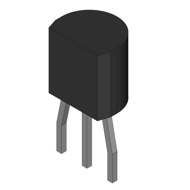


 工商网监
湘ICP备2023018690号
工商网监
湘ICP备2023018690号
