MR750 SERIES
MR754 and MR760 are Preferred Devices
High Current Lead
Mounted Rectifiers
Features
•
•
•
•
Current Capacity Comparable to Chassis Mounted Rectifiers
Very High Surge Capacity
Insulated Case
Pb−Free Packages are Available*
Mechanical Characteristics:
• Case: Epoxy, Molded
• Weight: 2.5 grams (approximately)
• Finish: All External Surfaces Corrosion Resistant and Terminal Lead
•
•
is Readily Solderable
Lead Temperature for Soldering Purposes:
260°C Max. for 10 Seconds
Polarity: Cathode Polarity Band
http://onsemi.com
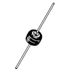
HIGH CURRENT
LEAD MOUNTED
SILICON RECTIFIERS
50 − 1000 VOLTS
DIFFUSED JUNCTION
AXIAL LEAD
BUTTON
CASE 194
STYLE 1
MARKING DIAGRAM
MR7xx AYYWWG
G
MR7 = Device Code
xx
= 50, 51, 52, 54, 56 or 60
A
= Location Code
YY
= Year
WW = Work Week
G
= Pb−Free Package
(Note: Microdot may be in either location)
ORDERING INFORMATION
See detailed ordering and shipping information in the package
dimensions section on page 6 of this data sheet.
Preferred devices are recommended choices for future use
and best overall value.
*For additional information on our Pb−Free strategy and soldering details, please
download the ON Semiconductor Soldering and Mounting Techniques
Reference Manual, SOLDERRM/D.
© Semiconductor Components Industries, LLC, 2007
March, 2007 − Rev. 6
1
Publication Order Number:
MR750/D
�MR750 SERIES
MAXIMUM RATINGS
Symbol
MR750
MR751
MR752
MR754
MR756
MR760
Unit
Peak Repetitive Reverse Voltage
Working Peak Reverse Voltage
DC Blocking Voltage
Characteristic
VRRM
VRWM
VR
50
100
200
400
600
1000
V
Non−Repetitive Peak Reverse Voltage
(Halfwave, single phase, 60 Hz peak)
VRSM
60
120
240
480
720
1200
V
VR(RMS)
35
70
140
280
420
700
V
RMS Reverse Voltage
Average Rectified Forward Current
(Single phase, resistive load, 60 Hz)
(See Figures 5 and 6)
IO
Non−Repetitive Peak Surge Current
(Surge applied at rated load conditions)
Operating and Storage Junction
Temperature Range
A
22 (TL = 60°C, 1/8 in Lead Lengths)
6.0 (TA = 60°C, P.C. Board mounting)
IFSM
A
400 (for 1 cycle)
TJ, Tstg
°C
*65 to +175
Stresses exceeding Maximum Ratings may damage the device. Maximum Ratings are stress ratings only. Functional operation above the
Recommended Operating Conditions is not implied. Extended exposure to stresses above the Recommended Operating Conditions may affect
device reliability.
ELECTRICAL CHARACTERISTICS
Characteristic and Conditions
Symbol
Max
Unit
Maximum Instantaneous Forward Voltage Drop (iF = 100 A, TJ = 25°C)
vF
1.25
V
Maximum Forward Voltage Drop (IF = 6.0 A, TA = 25°C, 3/8 in leads)
VF
0.90
V
Maximum Reverse Current
(Rated DC Voltage)
IR
25
1.0
�A
mA
TJ = 25°C
TJ = 100°C
http://onsemi.com
2
�MR750 SERIES
500
IFSM , PEAK HALF WAVE CURRENT (AMP)
700
TJ = 25°C
300
MAXIMUM
200
100
70
50
VRRM MAY BE APPLIED BETWEEN
EACH CYCLE OF SURGE. THE TJ
NOTED IS TJ PRIOR TO SURGE
400
300
25°C
175°C
200
25°C
TJ = 175°C
100
80
60
30
1.0
2.0
5.0
20
10
20
50
100
NUMBER OF CYCLES AT 60 Hz
Figure 2. Maximum Surge Capability
10
7.0
5.0
+0.5
3.0
0
COEFFICIENT (mV/° C)
iF, INSTANTANEOUS FORWARD CURRENT (AMP)
TYPICAL
600
2.0
1.0
0.7
0.5
TYPICAL RANGE
−0.5
−1.0
−1.5
0.3
0.2
−2.0
0.6
0.8
1.0
1.2
1.4
1.6
1.8
2.0
2.2
2.4
0.2
2.6
vF, INSTANTANEOUS FORWARD VOLTAGE (VOLTS)
1.0
2.0
5.0
10
20
50
100
200
iF, INSTANTANEOUS FORWARD CURRENT (AMP)
Figure 3. Forward Voltage Temperature Coefficient
Figure 1. Forward Voltage
R θJL(t) , JUNCTION−TO−LEAD TRANSIENT
THERMAL RESISTANCE (° C/W)
0.5
20
10
L
1/2"
3/8"
L
1/4"
5.0
1/8"
HEAT SINK
3.0
Both leads to heat sink, with lengths as shown. Variations in R�JL(t)
below 2.0 seconds are independent of lead connections of 1/8 inch
or greater, and vary only about ±20% from the values shown. Values for times greater than 2.0 seconds may be obtained by drawing
a curve, with the end point (at 70 seconds) taken from Figure 8, or
calculated from the notes, using the given curves as a guide. Either
typical or maximum values may be used. For R�JL(t) values at pulse
widths less than 0.1 second, the above curve can be extrapolated
down to 10 �s at a continuing slope.
2.0
1.0
0.5
0.3
0.2
0.1
0.2
0.3
0.5
0.7
1.0
2.0
3.0
5.0
7.0
t, TIME (SECONDS)
Figure 4. Typical Transient Thermal Resistance
http://onsemi.com
3
10
20
30
50
70
�IF(AV), AVERAGE FORWARD CURRENT (AMPS)
IF(AV), AVERAGE FORWARD CURRENT (AMPS)
MR750 SERIES
28
RESISTIVE INDUCTIVE
LOADS
L = 1/8"
24
1/4"
20
BOTH LEADS TO HEAT
SINK WITH LENGTHS
AS SHOWN
3/8"
16
12
5/8"
8.0
4.0
0
20
0
40
60
80
100
120
140
160
180
200
7.0
R�JA = 25°C/W
SEE NOTE
6.0
RESISTIVE INDUCTIVE LOADS
CAPACITANCE LOADS − 1� & 3�
5.0
I(pk) = 5 Iavg
I(pk) = 10 Iavg
I(pk) = 20 Iavg
4.0
3.0
R�JA = 40°C/W
2.0
1.0
0
f = 60 Hz
SEE NOTE
6� (IPK/IAVE = 6.28)
0
20
40
TL, LEAD TEMPERATURE (°C)
60
80
100
120
140
160
180
200
TA, AMBIENT TEMPERATURE (°C)
Figure 5. Maximum Current Ratings
Figure 6. Maximum Current Ratings
NOTES
THERMAL CIRCUIT MODEL
PF(AV), POWER DISSIPATION (WATTS)
32
(For Heat Conduction Through The Leads)
CAPACITANCE LOADS
I(pk) = 5 Iavg
28
24
10 Iavg
20
20 Iavg
6�
R�S(A)
1� & 3�
R�L(A)
R�J(A)
TA(A)
R�J(K)
R�L(K)
R�S(K)
TA(K)
PF
TL(A)
TC(A)
TJ
TC(K)
TL(K)
16
12
Use of the above model permits junction to lead thermal resistance for
any mounting configuration to be found. Lowest values occur when one
side of the rectifier is brought as close as possible to the heat sink as
shown below. Terms in the model signify:
TA = Ambient Temperature
TC = Case Temperature
TL = Lead Temperature
TJ = Junction Temperature
R�S = Thermal Resistance, Heat Sink to Ambient
R�L = Thermal Resistance, Lead to Heat Sink
R�J = Thermal Resistance, Junction to Case
PF = Power Dissipation
(Subscripts A and K refer to anode and cathode sides, respectively.)
Values for thermal resistance components are:
R�L = 40°C/W/in. Typically and 44°C/W/in Maximum.
R�J = 2°C/W typically and 4°C/W Maximum.
Since R�J is so low, measurements of the case temperature, TC, will be
approximately equal to junction temperature in practical lead mounted
applications. When used as a 60 Hz rectifierm the slow thermal response
holds TJ(PK) close to TJ(AVG). Therefore maximum lead temperature may
be found from: TL = 175°−R�JL PF. PF may be found from Figure 7.
The recommended method of mounting to a P.C. board is shown on the
sketch, where R�JA is approximately 25°C/W for a 1−1/2" x 1−1/2" copper
surface area. Values of 40°C/W are typical for mounting to terminal strips
or P.C. boards where available surface area is small.
RESISTIVE − INDUCTIVE LOADS
8.0
4.0
0
4.0
0
8.0
12
16
20
24
28
32
IF(AV), AVERAGE FORWARD CURRENT (AMPS)
Figure 7. Power Dissipation
R θJL , THERMAL RESISTANCE,
JUNCTION−TO−LEAD( ° C/W)
40
SINGLE LEAD TO HEAT SINK,
INSIGNIFICANT HEAT FLOW
THROUGH OTHER LEAD
35
30
25
ÉÉ
ÉÉ
ÉÉ
ÉÉ
ÉÉ
ÉÉ
ÉÉ
ÉÉ
20
15
10
BOTH LEADS TO HEAT
SINK, EQUAL LENGTH
5.0
0
0
1/8
1/4
3/8
1/2
5/8
3/4
7/8
1.0
L, LEAD LENGTH (INCHES)
Board Ground Plane
Recommended mounting for half wave circuit
Figure 8. Steady State Thermal Resistance
http://onsemi.com
4
�MR750 SERIES
30
t rr , REVERSE RECOVERY TIME (� s)
RELATIVE EFFICIENCY (%)
100
TJ = 25°C
70
TJ = 175°C
50
CURRENT INPUT WAVEFORM
30
20
1.0
2.0 3.0
5.0 7.0 10
20
30
50
20
TJ = 25°C
10
7.0
IF = 5 A
3A
1A
5.0
IF
3.0
0
2.0
trr
1.0
0.1
70 100
0.2
REPETITION FREQUENCY (kHz)
2.0
3.0
5.0 7.0 10
Figure 10. Reverse Recovery Time
1.0
t fr , FORWARD RECOVERY TIME (� s)
C, CAPACITANCE (pF)
0.5 0.7 1.0
0.3
IR/IF, RATIO OF REVERSE TO FORWARD CURRENT
Figure 9. Rectification Efficiency
1000
700
500
IR
TJ = 25°C
300
200
100
70
50
30
20
�f
TJ = 25°C
0.7
tfr
�fr
0.5
�fr = 1.0 V
0.3
0.2
�fr = 2.0 V
0.1
10
2.0
1.0
3.0
5.0 7.0 10
20
30
50
70 100
1.0
VR, REVERSE VOLTAGE (VOLTS)
3.0
5.0
7.0
10
IF, FORWARD PULSE CURRENT (AMP)
Figure 11. Junction Capacitance
Figure 12. Forward Recovery Time
For a square wave input of amplitude Vm, the efficiency
factor becomes:
RS
RL
VO
V2m
2R L
σ (square) + V2m .100% + 50%
RL
Figure 13. Single−Phase Half−Wave
Rectifier Circuit
V2o (dc)
RL
(1)
2o (dc)
V
.
.
σ+
+ V2o(rms) 100%+
100%
P (rms)
V 2o (ac) ) V 2o (dc)
RL
For a sine wave input Vm sin (wt) to the diode, assumed
lossless, the maximum theoretical efficiency factor becomes:
V2m
�2RL
σ (sine) + V2m .100% + 4 .100% + 40.6%
π2
4R L
(3)
(A full wave circuit has twice these efficiencies)
As the frequency of the input signal is increased, the
reverse recovery time of the diode (Figure 10) becomes
significant, resulting in an increasing AC voltage
component across RL which is opposite in polarity to the
forward current, thereby reducing the value of the efficiency
factor σ, as shown on Figure 9.
It should be emphasized that Figure 9 shows waveform
efficiency only; it does not provide a measure of diode
losses. Data was obtained by measuring the AC component
of Vo with a true rms AC voltmeter and the DC component
with a DC voltmeter. The data was used in Equation 1 to
obtain points for Figure 9.
The rectification efficiency factor σ shown in Figure 9
was calculated using the formula:
P (dc)
2.0
(2)
http://onsemi.com
5
�MR750 SERIES
ORDERING INFORMATION
Device
Package
MR750
Axial Lead
MR750G
Axial Lead
(Pb−Free)
MR750RL
Axial Lead
MR750RLG
Axial Lead
(Pb−Free)
MR751
Axial Lead
MR751G
Axial Lead
(Pb−Free)
MR751RL
Axial Lead
MR751RLG
Axial Lead
(Pb−Free)
MR752
Axial Lead
MR752G
Axial Lead
(Pb−Free)
MR752RL
Axial Lead
MR752RLG
Axial Lead
(Pb−Free)
MR754
Axial Lead
MR754G
Axial Lead
(Pb−Free)
MR754RL
Axial Lead
MR754RLG
Axial Lead
(Pb−Free)
MR756
Axial Lead
MR756G
Axial Lead
(Pb−Free)
MR756RL
Axial Lead
MR756RLG
Axial Lead
(Pb−Free)
MR760
Axial Lead
MR760G
Axial Lead
(Pb−Free)
MR760RL
Axial Lead
MR760RLG
Axial Lead
(Pb−Free)
Shipping †
1000 Units / Box
800 / Tape & Reel
1000 Units / Box
800 / Tape & Reel
1000 Units / Box
800 / Tape & Reel
1000 Units / Box
800 / Tape & Reel
1000 Units / Box
800 / Tape & Reel
1000 Units / Box
800 / Tape & Reel
†For information on tape and reel specifications, including part orientation and tape sizes, please refer to our Tape and Reel Packaging
Specifications Brochure, BRD8011/D.
http://onsemi.com
6
�MECHANICAL CASE OUTLINE
PACKAGE DIMENSIONS
MICRODE AXIAL
CASE 194−04
ISSUE H
DATE 09 SEP 2003
A
NOTES:
1. CATHODE SYMBOL ON PACKAGE.
2. 194−01 OBSOLETE, 194−04 NEW
STANDARD.
D
1
MILLIMETERS
INCHES
DIM MIN
MAX
MIN MAX
A
8.43
8.69 0.332 0.342
B
5.94
6.25 0.234 0.246
D
1.27
1.35 0.050 0.053
K 25.15 25.65 0.990 1.010
K
SCALE 1:1
B
K
2
GENERIC
MARKING DIAGRAM*
STYLE 1:
PIN 1. CATHODE
2. ANODE
DEV AYYWW
DEV
A
YY
WW
= Specific Device Code
= Assembly Location
= Year
= Work Week
*This information is generic. Please refer
to device data sheet for actual part
marking.
DOCUMENT NUMBER:
DESCRIPTION:
98ASB42126B
MICRODE AXIAL
Electronic versions are uncontrolled except when accessed directly from the Document Repository.
Printed versions are uncontrolled except when stamped “CONTROLLED COPY” in red.
PAGE 1 OF 1
ON Semiconductor and
are trademarks of Semiconductor Components Industries, LLC dba ON Semiconductor or its subsidiaries in the United States and/or other countries.
ON Semiconductor reserves the right to make changes without further notice to any products herein. ON Semiconductor makes no warranty, representation or guarantee regarding
the suitability of its products for any particular purpose, nor does ON Semiconductor assume any liability arising out of the application or use of any product or circuit, and specifically
disclaims any and all liability, including without limitation special, consequential or incidental damages. ON Semiconductor does not convey any license under its patent rights nor the
rights of others.
© Semiconductor Components Industries, LLC, 2019
www.onsemi.com
�onsemi,
, and other names, marks, and brands are registered and/or common law trademarks of Semiconductor Components Industries, LLC dba “onsemi” or its affiliates
and/or subsidiaries in the United States and/or other countries. onsemi owns the rights to a number of patents, trademarks, copyrights, trade secrets, and other intellectual property.
A listing of onsemi’s product/patent coverage may be accessed at www.onsemi.com/site/pdf/Patent−Marking.pdf. onsemi reserves the right to make changes at any time to any
products or information herein, without notice. The information herein is provided “as−is” and onsemi makes no warranty, representation or guarantee regarding the accuracy of the
information, product features, availability, functionality, or suitability of its products for any particular purpose, nor does onsemi assume any liability arising out of the application or use
of any product or circuit, and specifically disclaims any and all liability, including without limitation special, consequential or incidental damages. Buyer is responsible for its products
and applications using onsemi products, including compliance with all laws, regulations and safety requirements or standards, regardless of any support or applications information
provided by onsemi. “Typical” parameters which may be provided in onsemi data sheets and/or specifications can and do vary in different applications and actual performance may
vary over time. All operating parameters, including “Typicals” must be validated for each customer application by customer’s technical experts. onsemi does not convey any license
under any of its intellectual property rights nor the rights of others. onsemi products are not designed, intended, or authorized for use as a critical component in life support systems
or any FDA Class 3 medical devices or medical devices with a same or similar classification in a foreign jurisdiction or any devices intended for implantation in the human body. Should
Buyer purchase or use onsemi products for any such unintended or unauthorized application, Buyer shall indemnify and hold onsemi and its officers, employees, subsidiaries, affiliates,
and distributors harmless against all claims, costs, damages, and expenses, and reasonable attorney fees arising out of, directly or indirectly, any claim of personal injury or death
associated with such unintended or unauthorized use, even if such claim alleges that onsemi was negligent regarding the design or manufacture of the part. onsemi is an Equal
Opportunity/Affirmative Action Employer. This literature is subject to all applicable copyright laws and is not for resale in any manner.
PUBLICATION ORDERING INFORMATION
LITERATURE FULFILLMENT:
Email Requests to: orderlit@onsemi.com
onsemi Website: www.onsemi.com
◊
TECHNICAL SUPPORT
North American Technical Support:
Voice Mail: 1 800−282−9855 Toll Free USA/Canada
Phone: 011 421 33 790 2910
Europe, Middle East and Africa Technical Support:
Phone: 00421 33 790 2910
For additional information, please contact your local Sales Representative
�


 工商网监
湘ICP备2023018690号
工商网监
湘ICP备2023018690号
