NBC12430, NBC12430A 3.3V/5V Programmable PLL Synthesized Clock Generator
50 MHz to 800 MHz
The NBC12430 and NBC12430A are general purpose, PLL based synthesized clock sources. The VCO will operate over a frequency range of 400 MHz to 800 MHz. The VCO frequency is sent to the N−output divider, where it can be configured to provide division ratios of 1, 2, 4, or 8. The VCO and output frequency can be programmed using the parallel or serial interfaces to the configuration logic. Output frequency steps of 250 KHz, 500 KHz, 1.0 MHz, 2.0 MHz can be achieved using a 16 MHz crystal, depending on the output dividers settings. The PLL loop filter is fully integrated and does not require any external components.
Features http://onsemi.com MARKING DIAGRAMS
1 28
NBC12430xG PLCC−28 FN SUFFIX CASE 776 AWLYYWW
• • • • • • • • • •
• • −40°C to 85°C Ambient Operating Temperature (NBC12430A) • Pb−Free Packages are Available
Best−in−Class Output Jitter Performance, ±20 ps Peak−to−Peak 50 MHz to 800 MHz Programmable Differential PECL Outputs Fully Integrated Phase−Lock−Loop with Internal Loop Filter Parallel Interface for Programming Counter and Output Dividers During Powerup Minimal Frequency Overshoot Serial 3−Wire Programming Interface Crystal Oscillator Interface Operating Range: VCC = 3.135 V to 5.25 V CMOS and TTL Compatible Control Inputs Pin and Function Compatible with Motorola MC12430 and MPC9230 0°C to 70°C Ambient Operating Temperature (NBC12430)
LQFP−32 FA SUFFIX CASE 873A
NBC12 430x AWLYYWWG
1
1
32
QFN32 MN SUFFIX CASE 488AM
NBC12 430x AWLYYWWG G
x A WL, L YY, Y WW, W G or G
= Blank or A = Assembly Location = Wafer Lot = Year = Work Week = Pb−Free Package
(Note: Microdot may be in either location)
ORDERING INFORMATION
See detailed ordering and shipping information in the package dimensions section on page 16 of this data sheet.
© Semiconductor Components Industries, LLC, 2006
November, 2006 − Rev. 9
1
Publication Order Number: NBC12430/D
�NBC12430, NBC12430A
+3.3 or 5.0 V 1 MHz FREF with 16 MHz Crystal 1 PLL_VCC PHASE DETECTOR VCO 9−BIT B M COUNTER BN (1, 2, 4, 8) VCC 21, 25 24 23 FOUT FOUT
B 16 XTAL_SEL FREF_EXT 3 2 4 10−20MHz 5 OE S_LOAD P_LOAD 6 28 7 XTAL1 OSC XTAL2
+3.3 or 5.0 V
B2
400−800 MHz
20 LATCH LATCH
TEST
LATCH 0 1 0 2−BIT SR 1 3−BIT SR
S_DATA S_CLOCK
27 26
9−BIT SR
8 → 16 9 M[8:0]
17, 18 2 N[1:0]
22, 19
Figure 1. Block Diagram (PLCC−28) Table 1. Output Division
N [1:0] 00 01 10 11 Output Division 2 4 8 1
Table 2. XTAL_SEL And OE
Input XTAL_SEL OE 0 FREF_EXT Outputs Disabled 1 XTAL Outputs Enabled
http://onsemi.com
2
�NBC12430, NBC12430A
TEST
20
FOUT
FOUT
GND
25
24
23
22
21
S_CLOCK S_DATA S_LOAD PLL_VCC FREF_EXT XTAL_SEL XTAL1
GND
19 18 17 16 15 14 13 12
VCC
VCC
26 27 28 1 2 3 4 5 6 7 8 9 10 11
N[1] N[0] M[8] M[7] M[6] M[5] M[4]
XTAL2
P_LOAD
M[0]
M[1]
M[2]
Figure 2. 28−Lead PLCC (Top View)
TEST
FOUT
FOUT
GND
GND
VCC
VCC
VCC
M[3]
OE
TEST
26
FOUT
FOUT
GND
32
31
30
29
28
27
26
25 24 23 22 21 20 19 18 17
S_CLOCK S_DATA S_LOAD PLL_VCC PLL_VCC FREF_EXT XTAL_SEL XTAL1
1 2 3 4 5 6 7 8 9 10 11 12 13 14 15 16
N/C N[1] N[0] M[8] M[7]
32 31 30 29 28 27 25 24 23 22 21 20 19 18 17 9 10 11 12 13 14 15 16
GND
VCC
VCC
VCC
S_CLOCK S_DATA S_LOAD PLL_VCC
1 2 3 4 5 6 7 8
N/C N[1] N[0] M[8] M[7] M[6] M[5] M[4]
PLL_VCC M[6] FREF_EXT M[5] XTAL_SEL M[4] XTAL1
M[1]
M[2]
XTAL2
P_LOAD
M[0]
M[3]
N/C
OE
XTAL2
P_LOAD
M[0]
M[1]
M[2]
Figure 3. 32−Lead QFN (Top View)
Figure 4. 32−Lead LQFP (Top View)
http://onsemi.com
3
M[3]
N/C
OE
Exposed Pad (EP)
�NBC12430, NBC12430A
The following gives a brief description of the functionality of the NBC12430 and NBC12430A Inputs and Outputs. Unless explicitly stated, all inputs are CMOS/TTL compatible with either pullup or pulldown resistors. The PECL outputs are capable of driving two series terminated 50 W transmission lines on the incident edge.
ÁÁÁÁÁÁÁÁÁÁÁÁÁÁÁÁÁÁÁÁÁÁÁÁÁÁÁÁÁÁÁÁÁ
Pin Name Function Description INPUTS XTAL1, XTAL2 S_LOAD* Crystal Inputs CMOS/TTL Serial Latch Input (Internal Pulldown Resistor) CMOS/TTL Serial Data Input (Internal Pulldown Resistor) CMOS/TTL Serial Clock Input (Internal Pulldown Resistor) CMOS/TTL Parallel Latch Input (Internal Pullup Resistor) These pins form an oscillator when connected to an external series−resonant crystal. This pin loads the configuration latches with the contents of the shift registers. The latches will be transparent when this signal is HIGH; thus, the data must be stable on the HIGH−to−LOW transition of S_LOAD for proper operation. This pin acts as the data input to the serial configuration shift registers. This pin serves to clock the serial configuration shift registers. Data from S_DATA is sampled on the rising edge. This pin loads the configuration latches with the contents of the parallel inputs .The latches will be transparent when this signal is LOW; therefore, the parallel data must be stable on the LOW−to−HIGH transition of P_LOAD for proper operation. These pins are used to configure the PLL loop divider. They are sampled on the LOW−to−HIGH transition of P_LOAD. M[8] is the MSB, M[0] is the LSB. These pins are used to configure the output divider modulus. They are sampled on the LOW−to−HIGH transition of P_LOAD. Active HIGH Output Enable. The Enable is synchronous to eliminate possibility of runt pulse generation on the FOUT output. This pin can be used as the PLL Reference This pin selects between the crystal and the FREF_EXT source for the PLL reference signal. A HIGH selects the crystal input. S_DATA* S_CLOCK* P_LOAD** M[8:0]** N[1:0]** OE** FREF_EXT* XTAL_SEL** OUTPUTS FOUT, FOUT TEST POWER VCC PLL_VCC GND − Positive Supply for the Logic Positive Supply for the PLL Negative Power Supply Exposed Pad for QFN−32 only The positive supply for the internal logic and output buffer of the chip, and is connected to +3.3 V or +5.0 V. This is the positive supply for the PLL and is connected to +3.3 V or +5.0 V. These pins are the negative supply for the chip and are normally all connected to ground. The Exposed Pad (EP) on the QFN−32 package bottom is thermally connected to the die for improved heat transfer out of package. The exposed pad must be attached to a heat−sinking conduit. The pad is electrically connected to GND. PECL Differential Outputs PECL Output These differential, positive−referenced ECL signals (PECL) are the outputs of the synthesizer. The function of this output is determined by the serial configuration bits T[2:0]. CMOS/TTL PLL Loop Divider Inputs (Internal Pullup Resistor) CMOS/TTL Output Divider Inputs (Internal Pullup Resistor) CMOS/TTL Output Enable Input (Internal Pullup Resistor) CMOS/TTL Input (Internal Pulldown Resistor) CMOS/TTL Input (Internal Pullup Resistor) * When left Open, these inputs will default LOW. ** When left Open, these inputs will default HIGH.
PIN FUNCTION DESCRIPTION
http://onsemi.com
4
�NBC12430, NBC12430A
ATTRIBUTES
Characteristics Internal Input Pulldown Resistor Internal Input Pullup Resistor ESD Protection Human Body Model Machine Model Charged Device Model Pb Pkg PLCC LQFP QFN Flammability Rating Transistor Count Meets or exceeds JEDEC Spec EIA/JESD78 IC Latchup Test 1. For additional information, see Application Note AND8003/D. Oxygen Index: 28 to 34 Level 1 Level 2 Level 1 Value 75 kW 37.5 kW > 2 kV > 150 V > 1 kV Pb−Free Pkg Level 1 Level 2 Level 1
Moisture Sensitivity (Note 1)
UL 94 V−0 @ 0.125 in 2011
MAXIMUM RATINGS
Symbol VCC VI Iout TA Positive Supply Input Voltage Output Current Operating Temperature Range Parameter Condition 1 GND = 0 V GND = 0 V Continuous Surge NBC12430 NBC12430A VI � VCC Condition 2 Rating 6 6 50 100 0 to 70 −40 to +85 −65 to +150 0 lfpm 500 lfpm Standard Board 0 lfpm 500 lfpm Standard Board 0 lfpm 500 lfpm 2S2P Pb Pb−Free
很抱歉,暂时无法提供与“NBC12430AFNR2”相匹配的价格&库存,您可以联系我们找货
免费人工找货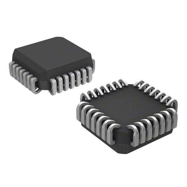


 工商网监
湘ICP备2023018690号
工商网监
湘ICP备2023018690号
