NBSG86A
2.5V/3.3V SiGe Differential
Smart Gate with Output
Level Select
The NBSG86A is a multi−function differential Logic Gate which
can be configured as an AND/NAND, OR/NOR, XOR/XNOR, or 2:1
MUX. This device is part of the GigaComm™ family of high
performance Silicon Germanium products. The device is housed in a
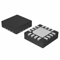
3 x 3 mm 16 pin QFN package.
Differential inputs incorporate internal 50 W termination resistors
and accept NECL (Negative ECL), PECL (Positive ECL),
LVCMOS/LVTTL, CML, or LVDS. The Output Level Select (OLS)
input is used to program the peak−to−peak output amplitude between
0 and 800 mV in five discrete steps.
The NBSG86A employs input default circuitry so that under open
input conditions (Dx, Dx, VTDx, VTDx, VTSEL) the outputs of the
device will remain stable.
Features
•
•
•
•
•
•
•
•
•
Maximum Input Clock Frequency > 8 GHz Typical
Maximum Input Data Rate > 8 Gb/s Typical
165 ps Typical Propagation Delay
40 ps Typical Rise and Fall Times
Selectable Swing PECL Output with Operating Range:
VCC = 2.375 V to 3.465 V with VEE = 0 V
Selectable Swing NECL Output with NECL Inputs with
Operating Range: VCC = 0 V with VEE = −2.375 V to −3.465 V
Selectable Output Level (0 V, 200 mV, 400 mV,
600 mV, or 800 mV Peak−to−Peak Output)
50 W Internal Input Termination Resistors
This is a Pb−Free Device
© Semiconductor Components Industries, LLC, 2014
January, 2018 − Rev. 20
1
www.onsemi.com
MARKING
DIAGRAM*
ÇÇ
16
1
1
QFN16
MN SUFFIX
CASE 485G
SG
86A
ALYWG
G
A
= Assembly Location
L
= Wafer Lot
Y
= Year
W
= Work Week
G
= Pb−Free Package
(Note: Microdot may be in either location)
*For additional marking information, refer to
Application Note AND8002/D.
ORDERING INFORMATION
See detailed ordering and shipping information on page 16 of
this data sheet.
Publication Order Number:
NBSG86A/D
�NBSG86A
VTD0 D0
16
OLS
1
SEL
2
15
D0
VTD0
14
13
Exposed Pad
(EP)
12
VEE
11
Q
NBSG86A
SEL
3
10
Q
VTSEL
4
9
VCC
5
6
VTD1
D1
7
8
D1 VTD1
Figure 1. QFN16 Pinout (Top View)
Table 1. Pin Description
Pin
Name
I/O
Description
1
OLS
(Note 3)
Input
2
SEL
ECL, CML, LVCMOS,
LVDS, LVTTL Input
Inverted Differential Select Logic Input.
3
SEL
ECL, CML, LVCMOS,
LVDS, LVTTL Input
Noninverted Differential Select Logic Input.
4
VTSEL
−
Common Internal 50 W Termination Pin for SEL/SEL. See Table 7. (Note 1)
5
VTD1
−
Internal 50 W termination pin. See Table 7. (Note 1)
6
D1
ECL, CML, LVCMOS,
LVDS, LVTTL Input
Noninverted Differential Input 1. Internal 75 kW to VEE.
7
D1
ECL, CML, LVCMOS,
LVDS, LVTTL Input
Inverted Differential Input 1. Internal 75 kW to VEE and 36.5 kW to VCC.
8
VTD1
−
Internal 50 W Termination Pin. See Table 7. (Note 1)
9
VCC
−
Positive Supply Voltage (Note 2)
10
Q
RSECL Output
Noninverted Differential Output. Typically Terminated with 50 W Resistor to VTT = VCC −
2 V.
11
Q
RSECL Output
Inverted Differential Output. Typically Terminated with 50 W Resistor to VTT = VCC − 2 V
12
VEE
−
Negative Supply Voltage (Note 2)
13
VTD0
−
Internal 50 W Termination Pin. See Table 7. (Note 1)
14
D0
ECL, CML, LVCMOS,
LVDS, LVTTL Input
Inverted Differential Input 0. Internal 75 kW to VEE and 36.5 kW to VCC.
15
D0
ECL, CML, LVCMOS,
LVDS, LVTTL Input
Noninverted Differential Input 0. Internal 75 kW to VEE.
16
VTD0
−
Internal 50 W Termination Pin. See Table 7. (Note 1)
−
EP
−
The Exposed Pad (EP) and the QFN−16 package bottom is thermally connected to the die
for improved heat transfer out of package. The exposed pad must be attached to a heat−
sinking conduit. The pad is electrically connected to the die but may be electrically and
thermally connected to VEE on the PC board.
Input Pin for the Output Level Select (OLS). See Table 2.
1. In the differential configuration when the input termination pins (VTDx, VTDx, VTSEL) are connected to a common termination voltage,
or left open, and if no signal is applied then the device will be susceptible to self−oscillation.
2. All VCC and VEE pins must be externally connected to Power Supply to guarantee proper operation.
3. When an output level of 400 mV is desired and VCC − VEE > 3.0 V, 2 kW resistor should be connected from OLS pin to VEE.
www.onsemi.com
2
�NBSG86A
Table 2. OUTPUT LEVEL SELECT OLS
Q/Q VPP
OLS Sensitivity
VCC
OLS
800 mV
OLS − 75 mV
VCC − 0.4 V
200 mV
OLS $ 150 mV
VCC − 0.8 V
600 mV
OLS $ 100 mV
VCC − 1.2 V
0
OLS $ 75 mV
VEE (Note 4)
400 mV
OLS $ 100 mV
Float
600 mV
N/A
4. When an output level of 400 mV is desired and VCC − VEE > 3.0 V, 2.0 kW resistor should be
connected from OLS to VEE.
50 W
VTD0
D0
R1
R2
D0
R1
VTD0
50 W
Q
50 W
Q
VTD1
D1
R1
R2
D1
50 W
R1
VTD1
50 W
50 W
VCC
VEE
VTSEL
SEL
SEL
Figure 2. Logic Diagram
50 W
VTD0
VT or
VBB
Table 3. AND/NAND TRUTH TABLE (Note 5)
D0
VCC
VTD0
�
b
�*b
D0
D1
SEL
Q
0
0
0
0
0
0
1
0
0
1
0
0
0
1
1
1
D0
50 W
Q
50 W
Q
VTD1
�
D1
5. D0, D1, SEL are inverse of D0, D1, SEL unless specified otherwise.
D1
VTD1
50 W
50 W
50 W
VTSEL
SEL
b
SEL
Figure 3. Configuration for AND/NAND Function
www.onsemi.com
3
�NBSG86A
50 W
VTD0
D0
�
Table 4. OR/NOR TRUTH TABLE**
D0
�
b
� or b
D0
D1
SEL
Q
0
1
0
0
VTD1
0
1
1
1
VCC
D1
1
1
0
1
VT or VBB
D1
1
1
1
1
VTD0
50 W
Q
50 W
Q
50 W
VTD1
50 W
50 W
** D0, D1, SEL are inverse of D0, D1, SEL unless specified
otherwise.
VTSEL
b
SEL
SEL
Figure 4. Configuration for OR/NOR Function
50 W
VTD0
D0
�
Table 5. XOR/XNOR TRUTH TABLE**
D0
VTD0
50 W
Q
50 W
Q
�
D1
SEL
Q
0
1
0
0
D1
0
1
1
1
D1
1
0
0
1
1
0
1
0
50 W
50 W
� XOR b
D0
VTD1
VTD1
b
50 W
** D0, D1, SEL are inverse of D0, D1, SEL unless specified otherwise.
VTSEL
b
SEL
SEL
Figure 5. Configuration for XOR/XNOR Function
50 W
VTD0
D0
D0
Table 6. 2:1 MUX TRUTH TABLE**
VTD0
50 W
Q
SEL
50 W
Q
1
D1
0
D0
VTD1
D1
Q
** D0, D1, SEL are inverse of D0, D1, SEL unless specified
otherwise.
D1
VTD1
50 W
50 W
50 W
VTSEL
SEL
SEL
Figure 6. Configuration for 2:1 MUX Function
www.onsemi.com
4
�NBSG86A
Table 7. Interfacing Options
INTERFACING OPTIONS
CONNECTIONS
CML
Connect VTD0, VTD1, VTSEL and VTD0, VTD1 to VCC
LVDS
Connect VTD0, VTD1, VTD0 and VTD1 together. Leave VTSEL open.
AC−COUPLED
Bias VTD0, VTD1, VTSEL and VTD0, VTD1 Inputs within (VIHCMR) Common Mode Range
RSECL, PECL, NECL
Standard ECL Termination Techniques
LVTTL, LVCMOS
An external voltage should be applied to the unused complementary differential input.
Nominal voltage 1.5 V for LVTTL and VCC/2 for LVCMOS inputs.
Table 8. ATTRIBUTES
Characteristics
Value
Internal Input Pulldown Resistors
(R1)
75 kW
Internal Input Pullup Resistor
(R2)
37.5 kW
Human Body Model
Machine Model
Charged Device Model
> 1 KV
> 50 V
> 4 KV
Pb−Free
Level 1
ESD Protection
Moisture Sensitivity (Note 6)
Flammability Rating
Oxygen Index: 28 to 34
UL 94 V−0 @ 0.125 in
Transistor Count
Meets or exceeds JEDEC Spec EIA/JESD78 IC Latchup Test
6. For additional information, see Application Note AND8003/D.
Table 9. MAXIMUM RATINGS
Symbol
Parameter
Condition 1
Condition 2
Rating
Unit
VCC
Positive Power Supply
VEE = 0 V
3.6
V
VEE
Negative Power Supply
VCC = 0 V
−3.6
V
VI
Positive Input
Negative Input
VEE = 0 V
VCC = 0 V
3.6
−3.6
V
V
VINPP
Differential Input Voltage |Dn − Dn|, |SEL − SEL|
VCC − VEE w 2.8 V
VCC − VEE < 2.8 V
2.8
|VCC − VEE|
V
V
IIN
Input Current Through RT (50 W Resistor)
Static
Surge
45
80
mA
mA
Iout
Output Current
Continuous
Surge
25
50
mA
mA
TA
Operating Temperature Range
−40 to +85
°C
Tstg
Storage Temperature Range
−65 to +150
°C
qJA
Thermal Resistance (Junction−to−Ambient)
(Note 7)
0 lfpm
500 lfpm
41.6
35.2
°C/W
°C/W
qJC
Thermal Resistance (Junction−to−Case)
2S2P (Note 7)
4.0
°C/W
Tsol
Wave Solder
< 3 sec @ 260°C
265
°C
Pb−Free
VI v VCC
VI w VEE
Stresses exceeding those listed in the Maximum Ratings table may damage the device. If any of these limits are exceeded, device functionality
should not be assumed, damage may occur and reliability may be affected.
7. JEDEC standard multilayer board − 2S2P (2 signal, 2 power) with 8 filled thermal vias under exposed pad.
www.onsemi.com
5
�NBSG86A
Table 10. DC CHARACTERISTICS, INPUT WITH LVPECL OUTPUT VCC = 2.5 V; VEE = 0 V, TA = −40°C to +85°C (Note 8)
−40°C
Symbol
25°C
85°C
Min
Typ
Max
Min
Typ
Max
Min
Typ
Max
Unit
23
30
39
23
30
39
23
30
39
mA
1460
1510
1560
1490
1540
1590
1515
1565
1615
mV
(OLS = VCC)
(OLS = VCC − 0.4 V)
(OLS = VCC − 0.8 V, OLS = FLOAT)
(OLS = VCC − 1.2 V)
(OLS = VEE)
555
1235
775
1455
1005
705
1295
895
1505
1095
855
1385
1015
1585
1215
595
1270
810
1490
1040
745
1330
930
1540
1130
895
1420
1050
1620
1250
625
1295
840
1510
1065
775
1355
960
1560
1155
925
1445
1080
1640
1275
Output Voltage Amplitude
(OLS = VCC)
(OLS = VCC − 0.4 V)
(OLS = VCC − 0.8 V, OLS = FLOAT)
(OLS = VCC − 1.2 V)
(OLS = VEE)
670
125
510
0
325
800
215
615
5
415
660
120
505
0
320
795
210
610
0
410
655
120
500
0
320
790
210
605
5
410
Characteristic
POWER SUPPLY CURRENT
IEE
Negative Power Supply Current
LVPECL OUTPUTS (Note 9)
VOH
Output HIGH Voltage
VOL
Output LOW Voltage
VOUTPP
mV
mV
DIFFERENTIAL CLOCK INPUTS DRIVEN SINGLE−ENDED (Figures 11 & 13) (Note 10)
VIH
Input HIGH Voltage (Single−Ended)
D, D, SEL, SEL
1200
VCC
1200
VCC
1200
VCC
mV
VIL
Input LOW Voltage (Single−Ended)
D, D, SEL, SEL
0
VCC −
150
0
VCC −
150
0
VCC −
150
mV
Vth
Input Threshold Reference Voltage
Range (Note 11)
950
VCC
–75
950
VCC
–75
950
VCC
–75
mV
VISE
Single−Ended Input Voltage (VIH –
VIL)
150
2600
150
2600
150
260
mV
DIFFERENTIAL INPUTS DRIVEN DIFFERENTIALLY (Figures 12 & 14) (Note 12)
VIHD
Differential Input HIGH Voltage (D, D,
SEL, SEL)
1200
VCC
1200
VCC
1200
VCC
mV
VILD
Differential Input LOW Voltage (D, D,
SEL, SEL)
0
VCC −
75
0
VCC −
75
0
VCC −
75
mV
VID
Differential Input Voltage (VIHD –
VILD) (D, D, SEL, SEL)
75
2600
75
2600
75
2600
mV
VIHCMR
Input HIGH Voltage Common Mode
Range (Differential Configuration)
(Note 13) (Figure 15)
1200
2500
1200
2500
1200
2500
mV
IIH
Input HIGH Current (@VIH)
D, D
SEL, SEL
30
5
100
50
30
5
100
50
30
5
100
50
mA
IIL
Input LOW Current (@VIL)
D, D
SEL, SEL
20
5
100
50
20
5
100
50
20
5
100
50
mA
50
55
50
55
50
55
W
TERMINATION RESISTORS
RTIN
Internal Input Termination Resistor
45
45
45
Product parametric performance is indicated in the Electrical Characteristics for the listed test conditions, unless otherwise noted. Product
performance may not be indicated by the Electrical Characteristics if operated under different conditions.
NOTE: Device will meet the specifications after thermal equilibrium has been established when mounted in a test socket or printed circuit
board with maintained transverse airflow greater than 500 lfpm.
8. Input and output parameters vary 1:1 with VCC.
9. LVPECL outputs loaded with 50 W to VCC − 2 V for proper operation.
10. Vth, VIH, VIL,, and VISE parameters must be complied with simultaneously.
11. Vth is applied to the complementary input when operating in single−ended mode. Vth = (VIH − VIL) / 2.
12. VIHD, VILD, VID and VCMR parameters must be complied with simultaneously.
13. VIHCMR min varies 1:1 with VEE, VIHCMR max varies 1:1 with VCC. The VIHCMR range is referenced to the most positive side of the differential input signal.
www.onsemi.com
6
�NBSG86A
Table 11. DC CHARACTERISTICS, INPUT WITH LVPECL OUTPUT VCC = 3.3 V; VEE = 0 V, TA = −40°C to +85°C (Note 14)
−40°C
Symbol
Characteristic
25°C
85°C
Min
Typ
Max
Min
Typ
Max
Min
Typ
Max
Unit
23
30
39
23
30
39
23
30
39
mA
2260
2310
2360
2290
2340
2390
2315
2365
2415
mV
1320
2030
1550
2260
1785
1470
2090
1670
2310
1875
1620
2180
1790
2390
1995
1360
2065
1585
2290
1820
1510
2125
1705
2340
1910
1660
2215
1825
2420
2030
1390
2090
1615
2315
1850
1540
2150
1735
2365
1940
1690
2240
1855
2445
2060
705
130
535
0
345
815
220
640
0
435
695
125
530
0
340
805
215
635
0
430
690
125
525
0
335
800
215
630
0
425
POWER SUPPLY CURRENT
IEE
Negative Power Supply Current
LVPECL OUTPUTS (Note 15)
VOH
Output HIGH Voltage
VOL
Output LOW Voltage
mV
(OLS = VCC)
(OLS = VCC − 0.4 V)
(OLS = VCC − 0.8 V, OLS = FLOAT)
(OLS = VCC − 1.2 V)
**(OLS = VEE)
VOUTPP
Output Amplitude Voltage
mV
(OLS = VCC)
(OLS = VCC − 0.4 V)
(OLS = VCC − 0.8 V, OLS = FLOAT)
(OLS = VCC − 1.2 V)
**(OLS = VEE)
DIFFERENTIAL CLOCK INPUTS DRIVEN SINGLE−ENDED (Figures 11 & 13) (Note 16)
VIH
Input HIGH Voltage (Single−Ended)
D, D, SEL, SEL
1200
VCC
1200
VCC
1200
VCC
mV
VIL
Input LOW Voltage (Single−Ended)
D, D, SEL, SEL
0
VCC−
150
0
VCC−
150
0
VCC−
150
mV
Vth
Input Threshold Reference Voltage Range
(Note 17)
950
VCC
–75
950
VCC
–75
950
VCC
–75
mV
VISE
Single−Ended Input Voltage (VIH – VIL)
150
2600
150
2600
150
2600
mV
DIFFERENTIAL INPUTS DRIVEN DIFFERENTIALLY (Figures 12 & 14) (Note 18)
VIHD
Differential Input HIGH Voltage (D, D,
SEL, SEL)
VILD
1200
VCC
1200
VCC
1200
VCC
mV
Differential Input LOW Voltage (D, D, SEL,
SEL)
0
VCC −
75
0
VCC −
75
0
VCC −
75
mV
VID
Differential Input Voltage (VIHD – VILD) (D,
D, SEL, SEL)
75
2600
75
2600
75
2600
mV
VIHCMR
Input HIGH Voltage Common Mode
Range (Differential Configuration)
(Note 19) (Figure 19)
1200
3300
1200
3300
1200
3300
mV
IIH
Input HIGH Current (@VIH)
D, D
SEL, SEL
30
5
100
50
30
5
100
50
30
5
100
50
mA
IIL
Input LOW Current (@VIL)
D, D
SEL, SEL
20
5
100
50
20
5
100
50
20
5
100
50
mA
50
55
50
55
50
55
W
TERMINATION RESISTORS
RTIN
Internal Input Termination Resistor
45
45
45
Product parametric performance is indicated in the Electrical Characteristics for the listed test conditions, unless otherwise noted. Product
performance may not be indicated by the Electrical Characteristics if operated under different conditions.
NOTE: Device will meet the specifications after thermal equilibrium has been established when mounted in a test socket or printed circuit
board with maintained transverse airflow greater than 500 lfpm.
**When an output level of 400 mV is desired and VCC − VEE > 3.0 V, a 2 kW resistor should be connected from OLS to VEE.
14. Input and output parameters vary 1:1 with VCC.
15. LVPECL outputs loaded with 50 W to VCC − 2 V for proper operation.
16. Vth, VIH, VIL,, and VISE parameters must be complied with simultaneously.
17. Vth is applied to the complementary input when operating in single−ended mode. Vth = (VIH − VIL) / 2.
18. VIHD, VILD, VID and VCMR parameters must be complied with simultaneously.
19. VIHCMR min varies 1:1 with VEE, VIHCMR max varies 1:1 with VCC. The VIHCMR range is referenced to the most positive side of the differential input signal.
www.onsemi.com
7
�NBSG86A
Table 12. DC CHARACTERISTICS, NECL INPUT WITH NECL OUTPUT VCC = 0 V; VEE = −3.465 V to −2.375 V, TA = −40°C
to +85°C (Note 20)
−40°C
Symbol
Characteristic
25°C
85°C
Min
Typ
Max
Min
Typ
Max
Min
Typ
Max
Unit
23
30
39
23
30
39
23
30
39
mA
−1040
−990
−940
−1010
−960
−910
−985
−935
−885
mV
POWER SUPPLY CURRENT
IEE
Negative Power Supply Current
LVPECL OUTPUTS (Note 21)
VOH
Output HIGH Voltage
VOL
Output LOW Voltage
−3.465 V v VEE v −3.0 V
(OLS = VCC)
(OLS = VCC − 0.4 V)
(OLS = VCC − 0.8 V, OLS =FLOAT)
(OLS = VCC − 1.2 V)
**(OLS = VEE)
−3.0 V < VEE v −2.375 V
(OLS = VCC)
(OLS = VCC − 0.4 V)
(OLS = VCC − 0.8 V, OLS =FLOAT)
(OLS = VCC − 1.2 V)
(OLS = VEE)
VOUTPP
Output Voltage Amplitude
−3.465 V v VEE v −3.0 V
(OLS = VCC)
(OLS = VCC − 0.4 V)
(OLS = VCC − 0.8 V, OLS = FLOAT)
(OLS = VCC − 1.2 V)
**(OLS = VEE)
−3.0 V < VEE v −2.375 V
(OLS = VCC)
(OLS = VCC − 0.4 V)
(OLS = VCC − 0.8 V, OLS =FLOAT)
(OLS = VCC − 1.2 V)
(OLS = VEE)
mV
−1980
−1270
−1750
−1040
−1515
−1830
−1210
−1630
−990
−1425
−1680
−1120
−1510
−910
−1305
−1940
−1235
−1715
−1010
−1480
−1790
−1175
−1595
−960
−1390
−1640
−1085
−1475
−880
−1270
−1910
−1210
−1685
−985
−1450
−1760
−1150
−1565
−935
−1360
−1610
−1060
−1445
−855
−1240
−1945
−1265
−1725
−1045
−1495
−1795
−1205
−1605
−995
−1405
−1645
−1115
−1485
−915
−1285
−1905
−1230
−1690
−1010
−1460
−1755
−1170
−1570
−960
−1370
−1605
−1080
−1450
−880
−1250
−1875
−1205
−1660
−990
−1435
−1725
−1145
−1540
−940
−1345
−1575
−1055
−1420
−860
−1225
mV
705
130
535
0
345
815
220
640
0
435
695
125
530
0
340
805
215
635
0
430
690
125
525
0
335
800
215
630
0
425
670
125
510
0
325
800
215
615
5
415
660
120
505
0
320
795
210
610
0
410
655
120
500
0
320
790
210
605
5
410
DIFFERENTIAL CLOCK INPUTS DRIVEN SINGLE−ENDED (Figures 11 & 13) (Note 22)
VIH
Input HIGH Voltage (Single−Ended)
D, D, SEL, SEL
VEE +
1200
VCC
VEE +
1200
VCC
VEE +
1200
VCC
mV
VIL
Input LOW Voltage (Single−Ended)
D, D, SEL, SEL
VEE
VIH−
150
VEE
VIH−
150
VEE
VIH−
150
mV
Vth
Input Threshold Reference Voltage
Range (Note 23)
VEE +
950
VCC
–75
VEE +
950
VCC
–75
VEE +
950
VCC
–75
mV
VISE
Single−Ended Input Voltage (VIH – VIL)
150
2600
150
2600
150
2600
mV
Product parametric performance is indicated in the Electrical Characteristics for the listed test conditions, unless otherwise noted. Product
performance may not be indicated by the Electrical Characteristics if operated under different conditions.
NOTE: Device will meet the specifications after thermal equilibrium has been established when mounted in a test socket or printed circuit
board with maintained transverse airflow greater than 500 lfpm.
**When an output level of 400 mV is desired and VCC − VEE > 3.0 V, a 2 kW resistor should be connected from OLS to VEE.
20. Input and output parameters vary 1:1 with VCC.
21. LVPECL outputs loaded with 50 W to VCC − 2 V for proper operation.
22. Vth, VIH, VIL,, and VISE parameters must be complied with simultaneously.
23. Vth is applied to the complementary input when operating in single−ended mode. Vth = (VIH − VIL) / 2.
24. VIHD, VILD, VID and VCMR parameters must be complied with simultaneously.
25. VIHCMR min varies 1:1 with VEE, VIHCMR max varies 1:1 with VCC. The VIHCMR range is referenced to the most positive side of the differential input signal.
www.onsemi.com
8
�NBSG86A
Table 12. DC CHARACTERISTICS, NECL INPUT WITH NECL OUTPUT VCC = 0 V; VEE = −3.465 V to −2.375 V, TA = −40°C
to +85°C (Note 20)
−40°C
Symbol
Min
Characteristic
25°C
Typ
Max
Min
Typ
85°C
Max
Min
Typ
Max
Unit
DIFFERENTIAL INPUTS DRIVEN DIFFERENTIALLY (Figures 12 & 14) (Note 24)
VIHD
Differential Input HIGH Voltage (D, D,
SEL, SEL)
VEE+
1200
VCC
VEE+
1200
VCC
VEE+
1200
VCC
mV
VILD
Differential Input LOW Voltage (D, D,
SEL, SEL)
VEE
VCC −
75
VEE
VCC −
75
VEE
VCC −
75
mV
VID
Differential Input Voltage (VIHD – VILD)
(D, D, SEL, SEL)
75
2600
75
2600
75
2600
mV
VIHCMR
Input HIGH Voltage Common Mode
Range (Differential Configuration)
(Note 25) (Figure 15)
VEE+
1200
0
VEE+
1200
0
VEE+
1200
0
mV
IIH
Input HIGH Current (@VIH)
D, D
SEL, SEL
30
5
100
50
30
5
100
50
30
5
100
50
mA
IIL
Input LOW Current (@VIL)
D, D
SEL, SEL
20
5
100
50
20
5
100
50
20
5
100
50
mA
50
55
50
55
50
55
W
TERMINATION RESISTORS
RTIN
Internal Input Termination Resistor
45
45
45
Product parametric performance is indicated in the Electrical Characteristics for the listed test conditions, unless otherwise noted. Product
performance may not be indicated by the Electrical Characteristics if operated under different conditions.
NOTE: Device will meet the specifications after thermal equilibrium has been established when mounted in a test socket or printed circuit
board with maintained transverse airflow greater than 500 lfpm.
**When an output level of 400 mV is desired and VCC − VEE > 3.0 V, a 2 kW resistor should be connected from OLS to VEE.
20. Input and output parameters vary 1:1 with VCC.
21. LVPECL outputs loaded with 50 W to VCC − 2 V for proper operation.
22. Vth, VIH, VIL,, and VISE parameters must be complied with simultaneously.
23. Vth is applied to the complementary input when operating in single−ended mode. Vth = (VIH − VIL) / 2.
24. VIHD, VILD, VID and VCMR parameters must be complied with simultaneously.
25. VIHCMR min varies 1:1 with VEE, VIHCMR max varies 1:1 with VCC. The VIHCMR range is referenced to the most positive side of the differential input signal.
www.onsemi.com
9
�NBSG86A
Table 13. AC CHARACTERISTICS
VCC = 0 V; VEE = −3.465 V to −2.375 V or VCC = 2.375 V to 3.465 V; VEE = 0 V
−40°C
25°C
Min
Typ
Min
Typ
Min
Typ
7
8
7
8
7
8
GHz
fin v 7 GHz
fin = 8 GHz
590
270
730
440
470
230
720
420
540
180
700
390
mV
mV
tPLH,
tPHL
Propagation Delay to Output Differential
(Figure 16)
D/SEL → Q
110
160
210
115
165
215
120
170
220
tSKEW
Duty Cycle Skew (Note 27)
5
15
5
15
5
15
ps
tSKEW
Channel Skew
5
20
5
20
5
20
ps
tS
Set−Up Time (Dx to SEL)
30
30
30
ps
tH
Hold−Up Time (Dx to SEL)
35
35
35
ps
tJITTER
RMS Random Clock Jitter
(See Figure 7) (Note 29)
Symbol
Characteristic
fmax
Maximum Input Clock Frequency
(See Figure 7) (Note 26)
VOUTPP
Output Voltage Amplitude
(OLS = VCC)
tr
tf
Output Rise/Fall Times (20% − 80%)
@ 1 GHz
Max
Unit
ps
fin v 7 GHz
Peak−to−Peak Data Dependent Jitter
(Note 30)
fin v 7 Gb/s
Input Voltage Swing/Sensitivity
(Differential Configuration) (Note 28)
Max
ps
Q → D/SEL
VINPP
Max
85°C
0.5
0.5
12
75
(Q, Q)
tr
tf
1.5
1.5
0.5
12
2600
75
60
65
30
17
1.5
12
2600
75
60
65
30
17
2600
mV
ps
30
17
45
35
45
35
45
35
60
65
Product parametric performance is indicated in the Electrical Characteristics for the listed test conditions, unless otherwise noted. Product
performance may not be indicated by the Electrical Characteristics if operated under different conditions.
26. Measured using a 500 mV source, 50% duty cycle clock source. All loading with 50 W to VCC − 2.0 V. Input edge rates 40 ps (20% − 80%).
27. tSKEW = |tPLH − tPHL| for a nominal 50% differential clock input waveform. See Figure 16.
28. VINPP (max) cannot exceed VCC − VEE.
29. Additive RMS jitter with 50% duty cycle clock signal at 7 GHz.
30. Additive Peak−to−Peak data dependent jitter with NRZ PRBS 231−1 data rate at 7 Gb/s.
www.onsemi.com
10
�NBSG86A
9
OLS = VCC
800
700
8
7
OLS = VCC − 0.8 V,
OLS = FLOAT
600
6
500
5
*OLS = VEE
400
4
300
3
OLS = VCC − 0.4 V
200
JITTEROUT ps (RMS)
OUTPUT VOLTAGE AMPLITUDE (mV)
900
2
100
1
RMS JITTER
0
0
1
2
3
4
5
6
7
8
9
0
10
INPUT FREQUENCY (GHz)
Figure 7. Output Voltage Amplitude (VOUTPP) / RMS Jitter vs.
Input Frequency (fin) for 2:1 MUX Mode (VCC − VEE = 2.5 V @ 25�C; Repetitive 1010 Input Data Pattern)
800
9
8
OLS = VCC
700
600
7
OLS = VCC − 0.8 V
OLS = FLOAT
6
5
500
*OLS = VEE
400
300
4
3
OLS = VCC − 0.4 V
200
JITTEROUT ps (RMS)
OUTPUT VOLTAGE AMPLITUDE (mV)
900
2
100
1
RMS JITTER
0
0
1
2
3
4
5
6
7
8
9
0
10
INPUT FREQUENCY (GHz)
Figure 8. Output Voltage Amplitude (VOUTPP) / RMS Jitter vs.
Input Frequency (fin) for 2:1 MUX Mode (VCC − VEE = 3.3 V @ 25�C; Repetitive 1010 Input Data Pattern)
*When an output level of 400 mV is desired and VCC − VEE > 3.0 V, a 2 kW resistor should be connected from OLS to VEE.
www.onsemi.com
11
�NBSG86A
300
200
100
IOLS (mA)
0
−100
−200
−300
−400
−500
−600
−700
VCC
VCC − 400
VCC − 800
VCC − 1200
VEE
VOLS (mV)
Figure 9. Typical OLS Input Current vs. OLS Input Voltage
(VCC − VEE = 3.3 V @ 25�C)
1000
VCC − 75
VOUTPP (mV)
800
VCC − 700
VCC − 900
600
VEE + 100
400
VCC − 250
VCC − 550
200
VCC − 1125
VCC − 1275
0
VCC
VCC − 400
VCC − 800
VCC − 1200
OLS (mV)
Figure 10. OLS Operating Area
www.onsemi.com
12
VEE
�NBSG86A
IN
VIH
Vth
IN
VIL
IN
IN
Vth
Figure 11. Differential Input Driven
Single−Ended
VCC
Vthmax
Figure 12. Differential Inputs
Driven Differentially
VIHmax
VILmax
Vth
VIH
Vth
VIL
IN
IN
IN
VIHD
VILD
VIHmin
Vthmin
VILmin
VEE
Figure 13. Vth Diagram
VCC
Figure 14. Differential Inputs Driven
Differentially
VIHDmax
VIHCMRmax
D
VINPP(D) = VIH(D) − VIL(D)
VINPP(D) = VIH(D) − VIL(D)
VILDmax
D
VIHCMR
VID = |VIHD(IN) − VILD(IN)|
VIHDtyp
VID = VIHD − VILD
IN
IN
Q
VOUTPP(Q) = VOH(Q) − VOL(Q)
VOUTPP(Q) = VOH(Q) − VOL(Q)
VILDtyp
Q
VIHDmin
VIHCMRmin
tPHL
tPLH
VILDmin
VEE
Figure 15. VIHCMR Diagram
Figure 16. AC Reference Measurement
SEL
tPHL
tPLH
Qx
Qx
Figure 17. SELx to Qx Timing Diagram
www.onsemi.com
13
�NBSG86A
APPLICATION INFORMATION
All NBSG86A inputs can accept PECL, CML, LVTTL, LVCMOS and LVDS signal levels. The limitations for differential
input signal (LVDS, PECL, or CML) are minimum input swing of 75 mV and the maximum input swing of 2500 mV. Within
these conditions, the input voltage can range from VCC to 1.2 V. Examples interfaces are illustrated below in a 50 W
environment (Z = 50 W). For output termination and interface, refer to application note AND8020/D.
Table 14. INTERFACING OPTIONS
Interfacing Options
Connections
CML
Connect VTD and VTD to VCC (See Figure 18)
LVDS
Connect VTD and VTD Together (See Figure 20)
AC−COUPLED
RSECL, PECL, NECL
LVTTL, LVCMOS
Bias VTD and VTD Inputs within Common Mode Range (VCMR) (See Figure 19)
Standard ECL Termination Techniques (See Figure 22)
An External Voltage (VTHR) should be Applied to the Unused Complementary Differential Input. Nominal
VTHR is 1.5 V for LVTTL and VCC / 2 for LVCMOS Inputs. This Voltage must be within the
VTHR Specification. (See Figure 21)
VCC
VCC
50 W
50 W
Z = 50 W
Q
CML
Driver
D
VCC
Z = 50 W
VCC
Q
VTD
50 W
VTD
50 W
NBSG86A
D
VEE
VEE
Figure 18. CML Interface
VCC
VCC
Z = 50 W
D
VBias*
PECL
Driver
Z = 50 W
Recommended RT Values
VCC
C
VBias*
C
VTD
50 W
NBSG86A
VTD
50 W
RT
RT
5.0 V 290 W
D
RT
3.3 V 150 W
2.5 V
80 W
VEE
VEE
VEE
*VBias must be within common mode range limits (VCMR)
Figure 19. PECL Interface
www.onsemi.com
14
�NBSG86A
VCC
VCC
Z = 50 W
D
50 W
VTD
LVDS
Driver
NBSG86A
VTD
Z = 50 W
50 W
D
VEE
VEE
Figure 20. LVDS Interface
VCC
VCC
Z = 50 W
D
LVTTL/
LVCMOS
Driver
No Connect*
VTD
50 W
NBSG86A
No Connect
VREF
VTD
50 W
Recommended VREF Values
VREF
D
LVCMOS VCC − VEE
2
*or 60 pF to GND
VEE
VCC
LVTTL
Figure 21. LVCMOS/LVTTL Interface
Q
Zo = 50 W
D
Receiver
Device
Driver
Device
Q
Zo = 50 W
D
50 W
50 W
VTT
VTT = VCC − 2.0 V
Figure 22. Typical Termination for Output Driver and Device Evaluation
(See Application Note AND8020/D − Termination of ECL Logic Devices.)
www.onsemi.com
15
1.5 V
�NBSG86A
ORDERING INFORMATION
Package Type
Shipping†
NBSG86AMNG
QFN16
(Pb−Free / Halide−Free)
123 Units / Rail
NBSG86AMNR2G
QFN16
(Pb−Free / Halide−Free)
3000 / Tape & Reel
NBSG86AMNHTBG
QFN16
(Pb−Free / Halide−Free)
100 / Tape & Reel
Device
†For information on tape and reel specifications, including part orientation and tape sizes, please refer to our Tape and Reel Packaging Specifications Brochure, BRD8011/D.
www.onsemi.com
16
�NBSG86A
PACKAGE DIMENSIONS
QFN16 3x3, 0.5P
CASE 485G
ISSUE F
D
PIN 1
LOCATION
A
B
ÇÇÇ
ÇÇÇ
ÇÇÇ
L
L1
DETAIL A
ALTERNATE TERMINAL
CONSTRUCTIONS
E
ÉÉÉ
ÉÉÉ
0.10 C
2X
EXPOSED Cu
0.10 C
2X
TOP VIEW
DETAIL B
0.05 C
NOTES:
1. DIMENSIONING AND TOLERANCING PER
ASME Y14.5M, 1994.
2. CONTROLLING DIMENSION: MILLIMETERS.
3. DIMENSION b APPLIES TO PLATED
TERMINAL AND IS MEASURED BETWEEN
0.25 AND 0.30 MM FROM TERMINAL.
4. COPLANARITY APPLIES TO THE EXPOSED
PAD AS WELL AS THE TERMINALS.
L
(A3)
ÉÉ
ÉÉ
ÇÇ
MOLD CMPD
A3
A1
DETAIL B
A
0.05 C
ALTERNATE
CONSTRUCTIONS
NOTE 4
A1
SIDE VIEW
C
SEATING
PLANE
16X
L
16X
0.58
D2
PACKAGE
OUTLINE
8
4
MILLIMETERS
MIN
NOM MAX
0.80
0.90
1.00
0.00
0.03
0.05
0.20 REF
0.18
0.24
0.30
3.00 BSC
1.65
1.75
1.85
3.00 BSC
1.65
1.75
1.85
0.50 BSC
0.18 TYP
0.30
0.40
0.50
0.15
0.00
0.08
RECOMMENDED
SOLDERING FOOTPRINT*
0.10 C A B
DETAIL A
DIM
A
A1
A3
b
D
D2
E
E2
e
K
L
L1
1
9
2X
E2
16X
2X
1.84 3.30
K
1
16X
16
e
e/2
BOTTOM VIEW
16X
0.30
b
0.10 C A B
0.05 C
0.50
PITCH
NOTE 3
DIMENSIONS: MILLIMETERS
*For additional information on our Pb−Free strategy and soldering
details, please download the ON Semiconductor Soldering and
Mounting Techniques Reference Manual, SOLDERRM/D.
GigaComm is a trademark of Semiconductor Components Industries, LLC.
ON Semiconductor and
are trademarks of Semiconductor Components Industries, LLC dba ON Semiconductor or its subsidiaries in the United States and/or other countries.
ON Semiconductor owns the rights to a number of patents, trademarks, copyrights, trade secrets, and other intellectual property. A listing of ON Semiconductor’s product/patent
coverage may be accessed at www.onsemi.com/site/pdf/Patent−Marking.pdf. ON Semiconductor reserves the right to make changes without further notice to any products herein.
ON Semiconductor makes no warranty, representation or guarantee regarding the suitability of its products for any particular purpose, nor does ON Semiconductor assume any liability
arising out of the application or use of any product or circuit, and specifically disclaims any and all liability, including without limitation special, consequential or incidental damages.
Buyer is responsible for its products and applications using ON Semiconductor products, including compliance with all laws, regulations and safety requirements or standards,
regardless of any support or applications information provided by ON Semiconductor. “Typical” parameters which may be provided in ON Semiconductor data sheets and/or
specifications can and do vary in different applications and actual performance may vary over time. All operating parameters, including “Typicals” must be validated for each customer
application by customer’s technical experts. ON Semiconductor does not convey any license under its patent rights nor the rights of others. ON Semiconductor products are not
designed, intended, or authorized for use as a critical component in life support systems or any FDA Class 3 medical devices or medical devices with a same or similar classification
in a foreign jurisdiction or any devices intended for implantation in the human body. Should Buyer purchase or use ON Semiconductor products for any such unintended or unauthorized
application, Buyer shall indemnify and hold ON Semiconductor and its officers, employees, subsidiaries, affiliates, and distributors harmless against all claims, costs, damages, and
expenses, and reasonable attorney fees arising out of, directly or indirectly, any claim of personal injury or death associated with such unintended or unauthorized use, even if such
claim alleges that ON Semiconductor was negligent regarding the design or manufacture of the part. ON Semiconductor is an Equal Opportunity/Affirmative Action Employer. This
literature is subject to all applicable copyright laws and is not for resale in any manner.
PUBLICATION ORDERING INFORMATION
LITERATURE FULFILLMENT:
Literature Distribution Center for ON Semiconductor
19521 E. 32nd Pkwy, Aurora, Colorado 80011 USA
Phone: 303−675−2175 or 800−344−3860 Toll Free USA/Canada
Fax: 303−675−2176 or 800−344−3867 Toll Free USA/Canada
Email: orderlit@onsemi.com
◊
N. American Technical Support: 800−282−9855 Toll Free
USA/Canada
Europe, Middle East and Africa Technical Support:
Phone: 421 33 790 2910
www.onsemi.com
17
ON Semiconductor Website: www.onsemi.com
Order Literature: http://www.onsemi.com/orderlit
For additional information, please contact your local
Sales Representative
NBSG86A/D
�


 工商网监
湘ICP备2023018690号
工商网监
湘ICP备2023018690号
