NCN8026AMNGEVB
NCN8026A Evaluation
Board User's Manual
http://onsemi.com
EVAL BOARD USER’S MANUAL
INTRODUCTION
This document gives a detailed description of the
NCN8026A Evaluation Board (QFN-24) with the bill of
materials (BOM), board schematic, and layout. The
appropriate laboratory test setups are also provided. The
NCN8026A Evaluation Board has been designed to help for
a quick evaluation of the NCN8026A Smart Card Interface
device.
This document has to be used with the NCN8026A
datasheet. The datasheet contains full technical details
regarding the NCN8026A specifications and operation. The
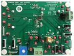
board (FR4 material) is implemented in two metal layers.
The top and bottom layers have thicknesses of 35 mm. The
PCB thickness is 1.6 mm with dimensions of 89 mm by
68 mm (see Figure 1).
Figure 1. Evaluation Board
TEST EQUIPMENT
The following equipment listed in Table 1 is suggested for the evaluation.
Table 1. TEST EQUIPMENT
Description
Regulated Power Supply
Example of Equipment (Note 1)
Main Features
200 mA DC current capability
Multimeter
Sourcemeter
Qty.
Tektronix PS2520G
2
Keithley 2000 or 2001
2
Keithley 2400
1
Oscilloscope
500 MHz bandwidth, four channel scope,
minimum 1MB memory per channel (Note 2)
Tektronix TDS744, 754 or 784 / TDS5054 series
or LeCroy WR5060, TDS5104B, 1 Ghz, 5 GS/s
1
Voltage probe
4 probes, 500MHz bandwidth
Tektronix or LeCroy
4
Waveform generator
Pattern generator
Agilent 81104A 80 MHz or HP8110A 150 MHz
2 outputs
1
SMB Cable
1
1. Equipment used in the context of this Evaluation Board User’s Manual
2. Greater scope memory per channel offers better resolution
© Semiconductor Components Industries, LLC, 2013
February, 2013 − Rev. 0
1
Publication Order Number:
EVBUM2174/D
�NCN8026AMNGEVB
TEST PROCEDURE
respectively. Refer to the recommended operating ranges for
VDD and VDDP in the datasheet. Use VDD = VDDP = 5 V
to get started.
Refer to Figure 2 for an overview of the main features of
the evaluation board.
Initial Setup
The initial setup given here is recommended before
starting measurements on the board.
• Set the CMDVCC/ in the OFF position (High).
• Set CS/ in the ON position: Chip selected, position
Low.
• Set CLKDIV1 and CLKDIV2 into low position (lowest
frequency FCLKIN )
• VESL0 and VSEL1 are used to change the output
CVCC (card power supply) or the smart card interface
mode which can be 1.8 V, 3.0 V or 5.0 V. Change
VSEL0 and VSEL1 using the switches (see Figure 2)
according to Table 2 below. When VSEL0 = 0 then
VSEL1 is in the mode 5 V / 3 Vbar, when VSEL0=1
then VSEL1 is in the mode 1.8 V / 3 Vbar. The initial
setup can be VSEL0 = 0 and VSEL1 = 1 for selecting
the 5 V mode. The CVCC output voltage can be
changed on the fly when the smart card interface is
active (/CMDVCC = Low). Nevertheless, it is
recommended to change CVCC after having
deactivated the device then reconfiguring CVCC by
setting the appropriate VSEL0 and VSEL1 and
reactivating the smart card interface.
Clock Frequency
CLKDIV1 and CLKDIV2 select the frequency divider for
the card clock CCLK according to Table 3 given below.
Table 3. CVCC PROGRAMMING
CLKDIV1
CLKDIV2
CCLK Frequency
1
0
fCLKIN / 1
1
1
fCLKIN / 2
0
1
fCLKIN / 4
0
0
fCLKIN / 8
The Clock
The clock is applied externally (SMB connector). Refer to
the datasheet for the recommended frequency and voltage
levels that can be applied at CLKIN.
Card Presence
The typical socket is normally open, so PRES/ has been
chosen; nevertheless the PRES and PRES/ test points can
also be used for signaling the presence of a card and starting
up the circuit. If not using a smart card, connect PRES/ to
ground.
Table 2. CVCC PROGRAMMING
Start the measurement
VSEL0
VSEL1
CVCC
0
0
3.0 V
0
1
5.0 V
1
0
3.0 V
1
1
1.8 V
To start the measurments, set the board as it follows:
1. Set CLKDIV1 and CLKDIV2 to select the correct
frequency.
2. Set VSEL0 and VSEL1 to select the correct output
voltage.
3. Check that the 1 kW potentiometer jumper is
turned to 1 kW.
4. Set /CS low.
5. Set CMDVCC/ high.
6. Check that VDD and VDDP are set to 5 V, and set
the current limit to 100 mA. Turn on the power
supplies VDD and VDDP.
7. Toggle /CMDVCC from High to Low to start the
device (activation sequence run).
8. Change the CVCC output voltage with the VSEL0
and VSEL1 switches.
9. Apply a clock to CLKIN and observe the card
clock at CCLK. Use CLKDIV1 and CLKDIV2 to
change the clock frequency.
• As a precaution, if using the built-in resistive load, turn
the 1 kW potentiometer to obtain a resistor output value
of 1 kW, and then connect the jumper.
DC Power Supplies
Two power supplies are used to bias the demo board.
VDDP is the input voltage of LDO Regulator. VDD is the
“digital” power supply which biases the input stages of the
NCN8026A device (control and signal inputs).
VDD and VDDP must be connected to the board to ensure
correct operation. Connect the VDD and VDDP power
supplies using the 2 pin male connectors J4 and J3
http://onsemi.com
2
�NCN8026AMNGEVB
EVALUATION BOARD DESCRIPTION
Figure 2. Board Description
http://onsemi.com
3
�NCN8026AMNGEVB
VSEL1
VSEL1
VSEL0
10K
TP20
CLKIN
TP3
/INT
TP22
RSTIN
TP15
VDD
1
1
1
TP4
I/OUC
1
TP5
AUX1UC
C9
C7
100n
3
PRESb
4
J4
J1
VDDP
0
6
IDDP
19
VSEL0
CLKIN
CSb
U1
INTb
VDDP
NCN8026A QFN−24
GND
PRESb
VDD
PRES
RSTIN
CI/O
CMDVCCb
7
J10
8
CAUX2
Standoffs
0
I/Ouc
20
AUX1uc
22
21
0R
PORADJ
VDDP
R3
0
C17
18
16
0
15
C6
100n
14
R2
R1
0R
open
330n
0
100K
J5
2
Ground
0
K2
CON1
0
0
1
I/O
J6
2
Ground
TP8
5
6
7
8
R11
1
0R
R12
0
0
1
0
0
J7
TP9
AUX2
1
TP7
AUX1
1
GND
VPP
I/O
C8
VCC
RST
CLK
C4
U2
SMART_CARD
0R
1k
R5
220n
1
2
3
4
1
R15 0R
1
TP11
RST
1
TP10
CLK
C12
80 pF
C13
80 pF
C14
80 pF
0
Figure 3. Board Schematic
http://onsemi.com
4
J8
1
R14 0R
0R
0
LOAD
2
VCC
R13
2
Ground
PORADJ
C5
VDD
1
CON1
TP1
1
9
J12
IDD
R8
10
J11
J3
0
K1
CON1
VDD
CMDVCCb
13
C11
CON1
0
22p
17
12
2
PRES 5
2
PRESb
1
CSb
CVCC
PRES
1
1
1
2
1
VDDP
VSEL0
CRST
TP19
PRES/
TP18
PRES
0
C2
100n
10u
1
11
C1
TP17
CCLK
SW6
9
0
CSb
AUX2uc
PGND
SW4
10
0
1
2
3
4
5
33p
CLKDIV1
25
CMDVCC/
VSEL1
0
C18
100n
CLKDIV1
C10
CSb
CLKDIV2
CLKDIV1
SW1
CLK_EXT_SMB
J9
I/Ouc
0
23
0
33p
24
C4
100n
CLKDIV1
CMDVCCb
SW2
J13
1
CLKDIV2
0
VSEL1
CLKDIV2
1
VDD
C8
33p
CLKDIV2
SW3
1
10K
C3
100n
VSEL0
TP6
AUX2UC
TP21
CMDVCCb
1
R16
1
TP13
CLKDIV1
1
R10
TP14
CLKDIV2
R9
10K
1
R7
10K
CAUX1
SW5
R6
10K
2
1
10K
TP2
VSEL1
R4
TP16
VSEL0
VDD
1
2
J2
VDD
1
1
0
TP23
CSb
EVALUATION BOARD SCHEMATIC
C15
C16
33 pF
100 pF
0
TP12
CVCC
�NCN8026AMNGEVB
BILL OF MATERIALS − NCN8026A EVALUATION BOARD
Table 4. BILL OF MATERIALS
Designator
Qty
Description
Value
Tol
Footprint
Manufacturer
Manufacturer Part #
Lead
Free
C1
1
CAP CER 10 UF 6.3 V
20% X5R 0805
10 uF
20%
0805
Murata
GRM21BR60J106ME19L
Yes
C2, C6, C7,
C18
3
CAP CER .1 UF 25 V
10% X7R 0805
100 nF
10%
0805
Murata
GRM21BR71E104KA01L
Yes
C3, C4
2
CAP CER .1 UF 25 V
10% X7R 0603
100 nF
10%
0603
Murata
GRM188R71E104KA01
Yes
C5
1
CAP CER .22 UF 16 V
X7R 10% 0805
220 nF
10%
0805
TDK Corporation
C2012X7R1C224K
Yes
C8, C9, C10,
C15
4
CAP CER 33 PF 16 V
X7R 0603
33 pF
5%
0603
AVX Corporation
Do not populate
Yes
C11
1
CAP CER .33 UF 16 V
X7R 10% 0805
330 nF
10%
0805
TDK Corporation
C2012X7R1C334K/1.25
Yes
C12, C13,
C14
3
Do not populate
80 pF
-
0603
Do not populate
Do not populate
-
C16
1
Do not populate
100 pF
-
0603
Do not populate
Do not populate
-
C17
1
CAP CERAMIC 22 PF
50 V NP0 0603
22 pF
5%
0603
Yageo
CC0603JRNP09BN220
Yes
R1
1
Do not populate
Open
-
0805
Do not populate
Do not populate
-
R2, R3, R11,
R12, R13,
R14, R15
7
RES 0.0 OHM 1/8 W
0603 SMD
0R
-
0603
Stackpole
Electronics Inc
RMCF0805ZT0R00
Yes
R4, R6, R7,
R9, R10, R16
5
CMS resistor 1%,
1/4 W
10k
1%
0603
Philips Components
232272461003
Yes
R5
1
Single turn Cermet
trimmer, 1k, 0.5 W,
10%
1k
-
CERMET-72PT
Bourns
3386F-102LF-ND
Yes
R8
1
CMS resistor 1%, 1/4
W
100k
1%
0805
Philips Components
232272461004
Yes
SW1 to SW6
5
PCB slide switches
-
-
INTER3-2,54
EAO
09.03290.01
Yes
TP1 to TP11,
TP13, TP14,
TP16, TP18
to TP21,
TP23
18
Clip Test Point, Hole
Diameter 1.0 mm
(0.040 mil)
-
-
TP_1.0MMHOLE_
KEYSTONE_5000
Keystone
5000
Yes
TP12, TP15,
TP17, TP22
4
Clip Test Point, Hole
Diameter 1.6 mm
(0.063 mil)
-
-
TP_1.6MMHOLE_
KEYSTONE_5010
Keystone
5010
Yes
J1,J2
2
VDD, VDDP, 2-Pins
Male Connector,
5.08 mm Step
-
-
MSTBA2
Phoenix Contact
MSTBA2.52G5.08
Yes
J3, J4, J8
3
IDD, IDDP, LOAD,
Breakable Single Row
Header (2 Pins)
-
-
CON2-2.54
TYCO Amp
5-826629-0
Yes
J5, J6, J7
3
Ground Strap, Brass,
Diameter 1.0 mm,
Pitch 10.16 mm,
Height 9.9 mm
-
-
GND_STRP
HARWIN
D3082-46
Yes
J9
1
SMB connector
-
-
SMB/V
IMS
111510001
Yes
U1
1
NCN8026A Smart Card
Interface
-
-
QFN 24 4X4
ENGINEERING
ON Semiconductor
NCN8026AMNTXG
Yes
U2
1
Smart card socket
-
-
SMARTCARD_FC
I_74343L0825S01
FCI
7434L0825S01LF
Yes
none
4
Standoff nut
-
-
STANDOFF
HOLE
Keystone
Electronics
1903C
Yes
none
4
Standoff screw
-
-
STANDOFF
HOLE
Keystone
Electronics
4814K-ND
Yes
http://onsemi.com
5
�onsemi,
, and other names, marks, and brands are registered and/or common law trademarks of Semiconductor Components Industries, LLC dba “onsemi” or its affiliates
and/or subsidiaries in the United States and/or other countries. onsemi owns the rights to a number of patents, trademarks, copyrights, trade secrets, and other intellectual property. A
listing of onsemi’s product/patent coverage may be accessed at www.onsemi.com/site/pdf/Patent−Marking.pdf. onsemi is an Equal Opportunity/Affirmative Action Employer. This
literature is subject to all applicable copyright laws and is not for resale in any manner.
The evaluation board/kit (research and development board/kit) (hereinafter the “board”) is not a finished product and is not available for sale to consumers. The board is only intended
for research, development, demonstration and evaluation purposes and will only be used in laboratory/development areas by persons with an engineering/technical training and familiar
with the risks associated with handling electrical/mechanical components, systems and subsystems. This person assumes full responsibility/liability for proper and safe handling. Any
other use, resale or redistribution for any other purpose is strictly prohibited.
THE BOARD IS PROVIDED BY ONSEMI TO YOU “AS IS” AND WITHOUT ANY REPRESENTATIONS OR WARRANTIES WHATSOEVER. WITHOUT LIMITING THE FOREGOING,
ONSEMI (AND ITS LICENSORS/SUPPLIERS) HEREBY DISCLAIMS ANY AND ALL REPRESENTATIONS AND WARRANTIES IN RELATION TO THE BOARD, ANY
MODIFICATIONS, OR THIS AGREEMENT, WHETHER EXPRESS, IMPLIED, STATUTORY OR OTHERWISE, INCLUDING WITHOUT LIMITATION ANY AND ALL
REPRESENTATIONS AND WARRANTIES OF MERCHANTABILITY, FITNESS FOR A PARTICULAR PURPOSE, TITLE, NON−INFRINGEMENT, AND THOSE ARISING FROM A
COURSE OF DEALING, TRADE USAGE, TRADE CUSTOM OR TRADE PRACTICE.
onsemi reserves the right to make changes without further notice to any board.
You are responsible for determining whether the board will be suitable for your intended use or application or will achieve your intended results. Prior to using or distributing any systems
that have been evaluated, designed or tested using the board, you agree to test and validate your design to confirm the functionality for your application. Any technical, applications or
design information or advice, quality characterization, reliability data or other services provided by onsemi shall not constitute any representation or warranty by onsemi, and no additional
obligations or liabilities shall arise from onsemi having provided such information or services.
onsemi products including the boards are not designed, intended, or authorized for use in life support systems, or any FDA Class 3 medical devices or medical devices with a similar
or equivalent classification in a foreign jurisdiction, or any devices intended for implantation in the human body. You agree to indemnify, defend and hold harmless onsemi, its directors,
officers, employees, representatives, agents, subsidiaries, affiliates, distributors, and assigns, against any and all liabilities, losses, costs, damages, judgments, and expenses, arising
out of any claim, demand, investigation, lawsuit, regulatory action or cause of action arising out of or associated with any unauthorized use, even if such claim alleges that onsemi was
negligent regarding the design or manufacture of any products and/or the board.
This evaluation board/kit does not fall within the scope of the European Union directives regarding electromagnetic compatibility, restricted substances (RoHS), recycling (WEEE), FCC,
CE or UL, and may not meet the technical requirements of these or other related directives.
FCC WARNING – This evaluation board/kit is intended for use for engineering development, demonstration, or evaluation purposes only and is not considered by onsemi to be a finished
end product fit for general consumer use. It may generate, use, or radiate radio frequency energy and has not been tested for compliance with the limits of computing devices pursuant
to part 15 of FCC rules, which are designed to provide reasonable protection against radio frequency interference. Operation of this equipment may cause interference with radio
communications, in which case the user shall be responsible, at its expense, to take whatever measures may be required to correct this interference.
onsemi does not convey any license under its patent rights nor the rights of others.
LIMITATIONS OF LIABILITY: onsemi shall not be liable for any special, consequential, incidental, indirect or punitive damages, including, but not limited to the costs of requalification,
delay, loss of profits or goodwill, arising out of or in connection with the board, even if onsemi is advised of the possibility of such damages. In no event shall onsemi’s aggregate liability
from any obligation arising out of or in connection with the board, under any theory of liability, exceed the purchase price paid for the board, if any.
The board is provided to you subject to the license and other terms per onsemi’s standard terms and conditions of sale. For more information and documentation, please visit
www.onsemi.com.
PUBLICATION ORDERING INFORMATION
LITERATURE FULFILLMENT:
Email Requests to: orderlit@onsemi.com
onsemi Website: www.onsemi.com
◊
TECHNICAL SUPPORT
North American Technical Support:
Voice Mail: 1 800−282−9855 Toll Free USA/Canada
Phone: 011 421 33 790 2910
www.onsemi.com
1
Europe, Middle East and Africa Technical Support:
Phone: 00421 33 790 2910
For additional information, please contact your local Sales Representative
�


 工商网监
湘ICP备2023018690号
工商网监
湘ICP备2023018690号
