Voltage Regulators, 1.0 A
Low-Dropout Positive,
Fixed and Adjustable
NCP1117LP
The NCP1117LP is the low power version of the popular NCP1117
family of low dropout voltage regulators, with reduced quiescent
current. It is intended primarily for high volume consumer
applications over the 0 to 125 degree temperature range. Capable of
providing an output current in excess of 1 A, with a dropout voltage of
1.3 V at 1 A full current load, the series consists of an adjustable and
five fixed voltage versions of 1.5 V, 1.8 V, 2.5 V, 3.3 V and 5.0 V.
Internal protection features consist of output current limiting and
built−in thermal shutdown. The NCP1117LP series can operate up to
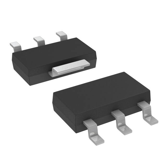
18 V max input voltage. The device is available in the popular
SOT−223 and DPAK packages.
www.onsemi.com
1
3
4
SOT−223
ST SUFFIX
CASE 318H
AYW
17Lxx G
G
Pin: 1. Adjust/Ground
2. Output
3. Input
Features
•
•
•
•
•
•
•
•
•
•
MARKING
DIAGRAM
Output Current in Excess of 1.0 A
1.4 V Maximum Dropout Voltage at 1 A
Quiescent Current over 10 times Lower than Traditional 1117
Fixed Output Voltages of 1.5 V, 1.8 V, 2.5 V, 3.3 V and 5.0 V
Adjustable Output Voltage Option
No Minimum Load Requirement for Fixed Voltage Output Devices
Good Noise Rejection
Current Limit and Thermal Shutdown Protection
Operation up to 18 V Input
These are Pb−Free Devices
1
2
3
Heatsink tab is connected to Pin 2.
xx
A
Y
W
G
= 15, 18, 25, 33, 50, AD
= Assembly Location
= Year
= Work Week
= Pb−Free Package
(Note: Microdot may be in either location)
4
1 2
DPAK
DT SUFFIX
CASE 369C
AYWW
XXX
XXXXXG
3
Applications
•
•
•
•
•
TV and Monitors
Set Top Boxes and Entertainment Devices
Switching Power Supply Post Regulation
Game Consoles and Consumer Applications
Hard Drive Controllers
ORDERING INFORMATION
See detailed ordering and shipping information in the package
dimensions section on page 12 of this data sheet.
TYPICAL APPLICATIONS
Input 3
Cin = 10 mF
NCP1117LP
2 Output
+
+
1
Cout = 10 mF
Input 3
Cin = 10 mF
Figure 1. Fixed
Output Regulator
© Semiconductor Components Industries, LLC, 2014
January, 2020 − Rev. 5
NCP1117LP
+
2 Output
+
1
Cout = 10 mF
Figure 2. Adjustable
Output Regulator
1
Publication Order Number:
NCP1117LP/D
�NCP1117LP
Figure 3. Block Diagram
Table 1. PIN FUNCTION DESCRIPTION
Pin No.
Pin Name
Description
1
Adj (GND)
2
Vout
The output of the regulator. A minimum of 10 mF capacitor (20 mW ≤ ESR ≤ 20 W) must be connected from this pin to ground to insure stability.
3
Vin
The input pin of regulator. Typically a large storage capacitor (20 mW ≤ ESR ≤ 20 W) is connected
from this pin to ground to insure that the input voltage does not sag below the minimum dropout
voltage during the load transient response. This pin must always be 1.3 V (typ.) higher than Vout in
order for the device to regulate properly.
A resistor divider from this pin to the Vout pin and ground sets the output voltage (Ground only for
Fixed−Mode).
Table 2. MAXIMUM RATINGS
Rating
Symbol
Value
DC Input Voltage
Vin
−0.3 to 18
V
Operating Junction Temperature Range
TOP
0 to 125
°C
Operating Ambient Temperature Range
TA
0 to 125
°C
Maximum Junction Temperature Range
TJ(max)
−55 to 150
°C
Power Dissipation and Thermal Characteristics
− Power Dissipation (Note 1)
− Thermal Resistance, Junction−to−Ambient (Note 2)
− Thermal Resistance, Junction−to−Case
PD
RqJA
RqJC
Internally Limited
108
15
W
°C/W
°C/W
Electrostatic Discharge
ESD
2000
V
Human Body Model
Machine Model
Storage Temperature Range
Unit
200
TSTG
−65 to 150
°C
NOTE: This device series contains ESD protection and exceeds the following tests:
ESD HBM tested per AEC−Q100−002 (EIA/JESD22−A114)
ESD MM tested per AEC−Q100−003 (EIA/JESD22−A115)
Latch–up Current Maximum Rating: ≤ 150mA per JEDEC standard: JESD78
Stresses exceeding those listed in the Maximum Ratings table may damage the device. If any of these limits are exceeded, device functionality
should not be assumed, damage may occur and reliability may be affected.
NOTE: All voltages are referenced to GND pin.
1. The maximum package power dissipation is:
PD +
T J(max) * T A
R qJA
2. RqJA on a 100 x 100 mm PCB Cu thickness 1 oz; TA = 25°C
www.onsemi.com
2
�NCP1117LP
Table 3. ELECTRICAL CHARACTERISTICS (Cin = 10 mF, Cout = 10 mF, for typical value TA = 25°C, for min and max values TA is
the operating ambient temperature range that applies unless otherwise noted.)
Conditions
Parameter
Symbol
Min
Typ
Max
Unit
Reference Voltage, Adjustable Output Devices
NCP1117−ADJ
TJ = 25°C
(Vin − Vout) = 1.5 V, Io = 10 mA
Vref
1.225
1.250
1.275
V
Output Voltage, Fixed
Output Devices
NCP1117−1.5
TJ = 25°C
3 V ≤ Vin ≤ 12 V, Io = 10 mA
Vout
1.470
1.5
1.530
V
NCP1117−1.8
TJ = 25°C
3.3 V ≤ Vin ≤ 12 V, Io = 10 mA
1.760
1.8
1.840
V
NCP1117−2.5
TJ = 25°C
4 V ≤ Vin ≤ 12 V, Io = 10 mA
2.450
2.5
2.550
V
NCP1117−3.3
TJ = 25°C
4.8 V ≤ Vin ≤ 12 V, Io = 10 mA
3.235
3.3
3.365
V
NCP1117−5.0
TJ = 25°C
6.5 V ≤ Vin ≤ 12 V, Io = 10 mA
4.900
5
5.100
V
Line Regulation,
Adjustable & Fixed
(Note 3)
NCP1117−XXX
TJ = 25°C
Vout + 1.5 V < Vin < 12 V,
Io = 10 mA
Regline
0.2
%
Load Regulation
(Note 3)
NCP1117−ADJ
TJ = 25°C
10 mA < Io < 1 A, Vin = 3.3 V
Regload
1
%
NCP1117−1.5
TJ = 25°C
10 mA < Io < 1 A, Vin = 3 V
12
15
mV
NCP1117−1.8
TJ = 25°C
10 mA < Io < 1 A, Vin = 3.3 V
15
18
mV
NCP1117−2.5
TJ = 25°C
10 mA < Io < 1 A, Vin = 4 V
20
25
mV
NCP1117−3.3
TJ = 25°C
10 mA < Io < 1 A, Vin = 4.7 V
26
33
mV
NCP1117−5.0
TJ = 25°C
10 mA < Io < 1 A, Vin = 6.5 V
40
50
mV
Dropout Voltage
(Vin – Vout),
Adjustable & Fixed
NCP1117−XXX
Iout = 1 A, TA = 25°C
DVout = Vout − 100 mV
1.3
1.4
V
Current Limit,
Adjustable & Fixed
NCP1117−XXX
Vin = 7 V, TA = 25°C
Iout
Minimum Load Current
(Note 4)
NCP1117−XXX
0°C ≤ Tj ≤ 125°C
ILmin
1
5
mA
Quiescent Current
NCP1117−fixed
Vin = 12 V
Io = 10 mA
IQFIX
550
700
mA
IQADJ
30
50
mA
0.008
0.04
%W
NCP1117−ADJ
Thermal Regulation
(Note 5)
TA = 25°C, T = 30 ms pulse
Ripple Rejection
NCP1117−XXX
Thermal Shutdown
Thermal Hysteresis
1.1
A
RR
60
dB
NCP1117−XXX
Tshdn
165
°C
NCP1117−XXX
Thyst
10
°C
F = 120 Hz, Cout = 25 mF tantalum,
Iout = 1 A, Vin = Vout + 3 V
Product parametric performance is indicated in the Electrical Characteristics for the listed test conditions, unless otherwise noted. Product
performance may not be indicated by the Electrical Characteristics if operated under different conditions.
3. Low duty cycle pulse techniques are used during testing to maintain the junction temperature as close to ambient as possible.
4. Guaranteed by design.
5. Thermal Regulation is defined as the change in output voltage at a time after a change in power dissipation is applied, excluding load or line
regulation effects. Specifications are for a current pulse equal to Iomax at VIN = VIN + 1.5 V for T = 30 msec. Guaranteed by characterization.
www.onsemi.com
3
�NCP1117LP
TYPICAL CHARACTERISTICS
1.25
1.36
1.20
DROPOUT VOLTAGE (V)
DROPOUT VOLTAGE (V)
1.34
1.15
1.10
1.05
1.32
1.30
1.28
1.26
1.24
1.22
1.20
1.00
−40
−20
0
20
40
60
80
100
1.18
−40
120
60
80
100
120
Figure 5. Dropout Voltage vs. Temperature
Iload = 1 A
0.45
OUTPUT VOLTAGE DEVIATION (%)
OUTPUT VOLTAGE DEVIATION (%)
40
Figure 4. Dropout Voltage vs. Temperature
Iload = 10 mA
0.090
0.085
0.080
0.075
0.070
0.065
0.060
−20
0
20
40
60
80
100
120
0.40
0.35
0.30
0.25
0.20
0.15
0.10
0.05
0
−40
−20
0
20
40
60
80
100
120
TA, AMBIENT TEMPERATURE (°C)
TA, AMBIENT TEMPERATURE (°C)
Figure 6. Line Regulation vs. Temperature
Iload = 10 mA
Figure 7. Load Regulation vs. Temperature
Iload = 1 A
OUTPUT SHORT CIRCUIT CURRENT (A)
1.510
1.508
OUTPUT VOLTAGE (V)
20
TA, AMBIENT TEMPERATURE (°C)
0.095
1.506
1.504
1.502
1.500
1.498
1.496
1.494
−40
0
TA, AMBIENT TEMPERATURE (°C)
0.100
0.055
0.050
−40
−20
−20
0
20
40
60
80
100
120
2.5
2.0
1.5
1.0
0.5
0
−40
−20
0
20
40
60
80
100
TA, AMBIENT TEMPERATURE (°C)
TA, AMBIENT TEMPERATURE (°C)
Figure 8. Output Voltage vs. Temperature
Iload = 10 mA
Figure 9. Output Short Circuit Current vs.
Temperature
www.onsemi.com
4
120
�NCP1117LP
570
1.21
560
1.20
DROPOUT VOLTAGE (V)
QUIESCENT CURRENT (mA)
TYPICAL CHARACTERISTICS
550
540
530
520
510
Vin = 12 V
Iload = 10 mA
Cin = Cout = 10 mF
500
490
480
−40
−20
0
20
40
60
80
100
1.17
1.16
1.15
1.14
DVout = Vout − 100 mV
Cin = Cout = 10 mF
TJ = 25°C
1.12
120
0.1 0.2
0.5
0.6
0.7
0.8
0.9
1.0
Figure 10. Quiescent Current vs. Temperature
Iload = 10 mA
Figure 11. Dropout Voltage vs. Output Current
100
Region of Stability
60
Vin = 3 V
Vout = 1.25 V
Cin = 10 mF MLCC
Cout = 10 mF MLCC
TJ = 25°C
OUTPUT CAPACITANCE (mF)
70
50
40
30
20
10
Region of Instability
0
0.2
0.4
0.6
Region of Instability
1.0
Vin = 3 V
Vout = 1.25 V
Iload = 5 mA − 1 A
Cin = 10 mF MLCC
TJ = 25°C
0.1
0.001
1.0
0.8
Region of Stability
10
Iout, OUTPUT CURRENT (A)
70
60
RR, RIPPLE REJECTION (dB)
70
60
50
40
fripple = 120 Hz
Cin = 22 mF Tantalum
Cout = 22 mF Tantalum
Vin − Vout = 3 V
TA = 25°C
20
10
0
100
0.1
1
ESR, EQUIVALENT SERIES RESISTANCE (W)
80
30
0.01
Figure 13. Output Capacitance vs. ESR
MLCC Capacitor
Figure 12. Equivalent Series Resistance vs.
Output Current − MLCC Capacitor
RR, RIPPLE REJECTION (dB)
0.4
Iout, OUTPUT CURRENT (A)
80
0
0.3
TA, AMBIENT TEMPERATURE (°C)
90
ESR (mW)
1.18
1.13
100
0
1.19
200 300 400 500 600 700 800 900 1000
50
40
30
fripple = 120 Hz
Cin = 22 mF Tantalum
Cout = 22 mF Tantalum
Vin − Vout = 3 V
TA = 25°C
20
10
0
0
100
200 300 400 500 600 700 800 900 1000
Iout, OUTPUT CURRENT (mA)
Iout, OUTPUT CURRENT (mA)
Figure 14. Ripple Rejection vs. Output Current
− 1.5 V
Figure 15. Ripple Rejection vs. Output Current
−5V
www.onsemi.com
5
�NCP1117LP
TYPICAL CHARACTERISTICS
450E−9
Cin = 10 mF Tantalum
Cout = 10 mF Tantalum
Vin − Vout = 3 V
0.5 Vpp
TA = 25°C
100
0.01 A
80
0.1 A
60
40
1A
300E−9
0.5 A
20
INPUT VOLTAGE (V)
1 V/ms
OUTPUT VOLTAGE
DEVIATION (mV)
0.1 A
250E−9
200E−9
150E−9
50E−9
4.0
3.0
100
1000
10000
100000
0
10
Cin = 10 mF Tantalum
Cout = 10 mF Tantalum
Vin − Vout = 3 V
TA = 25°C
100
1000
10000
100000 1000000
fripple, RIPPLE FREQUENCY (Hz)
FREQUENCY (Hz)
Figure 16. Ripple Rejection vs. Frequency −
Vout = 1.5 V
Figure 17. Output Spectral Noise Density vs.
Frequency − Vout = 1V5
Cin = 1.0 mF*
Cout = 10 mF*
Iout = 0.5 A
TA = 25°C
Cin = 1.0 mF*
Cout = 10 mF*
Iout = 0.1 A
TA = 25°C
50
0
−50
*Tantalum Capacitors
*Tantalum Capacitors
Figure 19. Line Transient Response − Vout = 1.5 V
Figure 18. Line Transient Response − Vout = 1.5 V
INPUT VOLTAGE (V)
1 V/ms
0.5 A
350E−9
100E−9
0
10
OUTPUT VOLTAGE
DEVIATION (mV)
1A
400E−9
V/sqrt (Hz)
RR, RIPPLE REJECTION (dB)
120
4.3
3.3
Cin = 1.0 mF*
Cout = 10 mF*
Iout = 0.1 A
TA = 25°C
Cin = 1.0 mF*
Cout = 10 mF*
Iout = 0.5 A
TA = 25°C
50
0
−50
*Tantalum Capacitors
*Tantalum Capacitors
Figure 20. Line Transient Response − Vout = 1.8 V
Figure 21. Line Transient Response − Vout = 1.8 V
www.onsemi.com
6
�NCP1117LP
OUTPUT VOLTAGE
DEVIATION (mV)
INPUT VOLTAGE (V)
1 V/ms
TYPICAL CHARACTERISTICS
5.0
4.0
Cin = 1.0 mF*
Cout = 10 mF*
Iout = 0.1 A
TA = 25°C
Cin = 1.0 mF*
Cout = 10 mF*
Iout = 0.5 A
TA = 25°C
50
0
−50
*Tantalum Capacitors
*Tantalum Capacitors
OUTPUT VOLTAGE
DEVIATION (mV)
INPUT VOLTAGE (V)
1 V/ms
Figure 22. Line Transient Response − Vout = 2.5 V
5.5
4.5
Cin = 1.0 mF*
Cout = 10 mF*
Iout = 0.1 A
TA = 25°C
Cin = 1.0 mF*
Cout = 10 mF*
Iout = 0.5 A
TA = 25°C
50
0
−50
*Tantalum Capacitors
*Tantalum Capacitors
INPUT VOLTAGE (V)
1 V/ms
Figure 24. Line Transient Response − Vout = 3.3 V
OUTPUT VOLTAGE
DEVIATION (mV)
Figure 23. Line Transient Response − Vout = 2.5 V
7.5
6.5
Figure 25. Line Transient Response − Vout = 3.3 V
Cin = 1.0 mF*
Cout = 10 mF*
Iout = 0.1 A
TA = 25°C
Cin = 1.0 mF*
Cout = 10 mF*
Iout = 0.5 A
TA = 25°C
50
0
−50
*Tantalum Capacitors
*Tantalum Capacitors
Figure 26. Line Transient Response − Vout = 5.0 V
Figure 27. Line Transient Response − Vout = 5.0 V
www.onsemi.com
7
�NCP1117LP
0.5
0.2
Cin = 10 mF*
Cout = 10 mF*
Vin = 3.3 V
Preload=0.1A
TA = 25°C
20
0
−20
*Tantalum Capacitors
OUTPUT VOLTAGE
LOAD CURRENT
DEVIATION (mV)
CHANGE (A) 0.5A/ms
OUTPUT VOLTAGE
LOAD CURRENT
DEVIATION (mV)
CHANGE (A) 0.5A/ms
TYPICAL CHARACTERISTICS
0.5
0.2
Cin = 10 mF*
Cout = 10 mF*
Vin = 3.3 V
Preload=0.1A
TA = 25°C
50
0
−50
*Tantalum Capacitors
0.2
20
0
−20
*Tantalum Capacitors
Figure 29. Load Transient Response − Vout = 2.5 V
OUTPUT VOLTAGE
LOAD CURRENT
DEVIATION (mV)
CHANGE (A) 0.5A/ms
OUTPUT VOLTAGE
LOAD CURRENT
DEVIATION (mV)
CHANGE (A) 0.5A/ms
Figure 28. Load Transient Response − Vout = 1.8 V
0.5
Cin = 10 mF*
Cout = 10 mF*
Vin = 3.3 V
Preload=0.1A
TA = 25°C
Figure 30. Load Transient Response − Vout = 3.3 V
0.5
0.2
Cin = 10 mF*
Cout = 10 mF*
Vin = 3.3 V
Preload=0.1A
TA = 25°C
50
0
−50
*Tantalum Capacitors
Figure 31. Load Transient Response − Vout = 5.0 V
www.onsemi.com
8
�NCP1117LP
TYPICAL CHARACTERISTICS
125
1.8
120
Power curve with PCB cu thk 2.0 oz
1.6
115
1.4
Power curve with PCB cu thk 1.0 oz
Theta JA (C/W)
105
1.2
100
95
Theta JA curve with PCB cu thk 1.0 oz
90
1.0
0.8
85
0.6
80
Theta JA curve with PCB cu thk 2.0 oz
75
0.4
70
0.2
65
60
0
Max Power (W)
110
100
200
300
Copper heat spreader area (mm^2)
400
0.0
500
Figure 32. SOT−223 Thermal Resistance and Maximum Power Dissipation vs. P.C.B. Copper Length
www.onsemi.com
9
�NCP1117LP
APPLICATIONS INFORMATION
Introduction
Frequency compensation for the regulator is provided by
capacitor Cout and its use is mandatory to ensure output
stability. A minimum capacitance value of 4.7 mF with an
equivalent series resistance (ESR) that is within the limits of
20 mW to 20 W is required. The capacitor type can be
ceramic, tantalum, or aluminum electrolytic as long as it
meets the minimum capacitance value and ESR limits over
the circuit’s entire operating temperature range. Higher
values of output capacitance can be used to enhance loop
stability and transient response with the additional benefit of
reducing output noise.
The NCP1117LP is a low dropout positive fixed or
adjustable mode regulator with 1 A output capability. This
LDO is guaranteed to have a significant reduction in dropout
voltage along with enhanced output voltage accuracy and
temperature stability when compared to older industry
standard three−terminal adjustable regulators.
These devices contain output current limiting, safe operating
area compensation and thermal shutdown protection
making them designer friendly for powering numerous
consumer and industrial products. The NCP1117LP series is
pin compatible with the older NCP1117.
Input
Output Voltage
The typical application circuits for the fixed and
adjustable output regulators are shown in Figures 33 and 34.
The adjustable devices are floating voltage regulators. They
develop and maintain the nominal 1.25 V reference voltage
between the output and adjust pins. The reference voltage is
programmed to a constant current source by resistor R1, and
this current flows through R2 to ground to set the output
voltage. The programmed current level is usually selected to
be greater than the specified 5.0 mA minimum that is
required for regulation. Since the adjust pin current, Iadj, is
significantly lower and constant with respect to the
programmed load current, it generates a small output
voltage error that can usually be ignored. For the fixed
output devices R1 and R2 are included within the device and
the ground current Ignd is 550 mA (typ).
Cin
Cin
NCP1117LP
+
+
1
Vref
1
R1
+
ǒ
+
Cout
Cadj
Ǔ
Vout + Vref 1 ) R2 ) R2 @ Iadj
R1
Figure 34. Adjustable Output Regulator
The output ripple will increase linearly for fixed and
adjustable devices as the ratio of output voltage to the
reference voltage increases. For example, with a 5 V
regulator, the output ripple will increase by 5 V/1.25 V or 4
and the ripple rejection will decrease by 20 log of this ratio
or 12 dB. The loss of ripple rejection can be restored to the
values shown with the addition of bypass capacitor Cadj,
shown in Figure 34. The reactance of Cadj at the ripple
frequency must be less than the resistance of R1. The value
of R1 can be selected to provide the minimum required load
current to maintain regulation and is usually in the range of
100 W to 200 W.
Cadj u
1
2p @ fripple @ R1
The minimum required capacitance can be calculated
from the above formula. When using the device in an
application that is powered from the AC line via a
transformer and a full wave bridge, the value for Cadj is:
Output
2
+
Output
2
R2
Input bypass capacitor Cin may be required for regulator
stability if the device is located more than a few inches from
the power source. This capacitor will reduce the circuit’s
sensitivity when powered from a complex source impedance
and significantly enhance the output transient response. The
input bypass capacitor should be mounted with the shortest
possible track length directly across the regulator’s input
and ground terminals. A 10 mF ceramic or tantalum
capacitor should be adequate for most applications.
3
NCP1117LP
Iadj
External Capacitors
Input
3
fripple + 120 Hz, R1 + 120 W, then Cadj u 11.1 mF
Cout
Ignd
The value for Cadj is significantly reduced in applications
where the input ripple frequency is high. If used as a post
regulator in a switching converter under the following
conditions:
Figure 33. Fixed Output Regulator
fripple + 50 kHz, R1 + 120 W, then Cadj u 0.027 mF
www.onsemi.com
10
�NCP1117LP
Protection Diodes
Input
The NCP1117LP family has two internal low impedance
diode paths that normally do not require protection when
used in the typical regulator applications. The first path
connects between Vout and Vin, and it can withstand a peak
surge current of about 15 A. Normal cycling of Vin cannot
generate a current surge of this magnitude. Only when Vin
is shorted or crowbarred to ground and Cout is greater than
50 mF, it becomes possible for device damage to occur.
Under these conditions, diode D1 is required to protect the
device. The second path connects between Cadj and Vout, and
it can withstand a peak surge current of about 150 mA.
Protection diode D2 is required if the output is shorted or
crowbarred to ground and Cadj is greater than 1.0 mF.
Cin
3
NCP1117LP
+
1
R2
R1
+
D2
+
+
Cin
RW+
2
R1
1
Output
Remote
Load
Cout
R2
RW−
Figure 36. Load Sensing
Thermal Considerations
This series contains an internal thermal limiting circuit
that is designed to protect the regulator in the event that the
maximum junction temperature is exceeded. When
activated, typically at 165°C, the regulator output switches
off and then back on as the die cools. As a result, if the device
is continuously operated in an overheated condition, the
output will appear to be oscillating. This feature provides
protection from a catastrophic device failure due to
accidental overheating. It is not intended to be used as a
substitute for proper heatsinking. The maximum device
power dissipation can be calculated by:
Output
2
NCP1117LP
+
D1
Input
3
Cout
Cadj
PD +
TJ(max) * TA
RqJA
The devices are available in surface mount SOT−223
package. This package has an exposed metal tab that is
specifically designed to reduce the junction to air thermal
resistance, RqJA, by utilizing the printed circuit board
copper as a heat dissipater. Figure 32 shows typical RqJA
values that can be obtained from a square pattern using
economical single sided 1.0 oz and 2.0 oz copper board
material. The final product thermal limits should be tested
and quantified in order to insure acceptable performance and
reliability. The actual RqJA can vary considerably from the
graphs shown. This will be due to any changes made in the
copper aspect ratio of the final layout, adjacent heat sources,
and air flow.
Figure 35. Protection Diode Placement
A combination of protection diodes D1 and D2 may be
required in the event that Vin is shorted to ground and Cadj
is greater than 50 mF. The peak current capability stated for
the internal diodes are for a time of 100 ms with a junction
temperature of 25°C. These values may vary and are to be
used as a general guide.
Load Regulation
The NCP1117LP series is capable of providing excellent
load regulation; but since these are three terminal devices,
only partial remote load sensing is possible. There are two
conditions that must be met to achieve the maximum
available load regulation performance. The first is that the
top side of programming resistor R1 should be connected as
close to the regulator case as practicable. This will minimize
the voltage drop caused by wiring resistance RW + from
appearing in series with reference voltage that is across R1.
The second condition is that the ground end of R2 should be
connected directly to the load. This allows true Kelvin
sensing where the regulator compensates for the voltage
drop caused by wiring resistance RW −.
Input
10
mF
3
NCP1117LP
2
R
+
Constant Current
Output
+
1
10
mF
V
Iout + ref ) Iadj
R
Figure 37. Constant Current Regulator
www.onsemi.com
11
�NCP1117LP
Input
Input
10
mF
3
+
R1
1
R2
Output
2
NCP1117LP
+
50 k
1N4001
2N2907
3
10
mF
10
mF
NCP1117LP
Output
2
+
R1
1
+
10
mF
R2
10
mF
2N2222
Output Voltage Control
Figure 38. Slow Turn−On Regulator
Resistor R2 sets the maximum output voltage. Each
transistor reduces the output voltage when turned on.
Figure 39. Digitally Controlled Regulator
Input
3
10
mF
Output Control
+
1
1.0 k
On
Off
NCP1117LP
2N2222
Output
2
120
+ 10
Input
10
mF
mF
3
NCP1117LP
+
1.0 k
mF
1
2.0 k
360
Output
5.0 V to
12 V
+ 10
2
+ 10
mF
Figure 41. Adjusting Output of Fixed
Voltage Regulators
Vout(Off) + Vref
Figure 40. Regulator with Shutdown
DEVICE ORDERING INFORMATION
Device
Package
Shipping†
SOT−223
(Pb−Free)
4000 / Tape & Reel
DPAK
(Pb−Free)
2500 / Tape & Reel
NCP1117LPST15T3G
NCP1117LPST18T3G
NCP1117LPST25T3G
NCP1117LPST33T3G
NCP1117LPST50T3G
NCP1117LPSTADT3G
NCP1117LPDT18RKG
NCP1117LPDT33RKG
NCP1117LPDTADJRKG
†For information on tape and reel specifications, including part orientation and tape sizes, please refer to our Tape and Reel Packaging
Specifications Brochure, BRD8011/D.
www.onsemi.com
12
�MECHANICAL CASE OUTLINE
PACKAGE DIMENSIONS
SOT−223
CASE 318H
ISSUE B
DATE 13 MAY 2020
SCALE 2:1
GENERIC
MARKING DIAGRAM*
AYW
XXXXXG
G
1
A
= Assembly Location
Y
= Year
W
= Work Week
XXXXX = Specific Device Code
G
= Pb−Free Package
(Note: Microdot may be in either location)
*This information is generic. Please refer to
device data sheet for actual part marking.
Pb−Free indicator, “G” or microdot “G”, may
or may not be present. Some products may
not follow the Generic Marking.
DOCUMENT NUMBER:
DESCRIPTION:
98ASH70634A
SOT−223
Electronic versions are uncontrolled except when accessed directly from the Document Repository.
Printed versions are uncontrolled except when stamped “CONTROLLED COPY” in red.
PAGE 1 OF 1
ON Semiconductor and
are trademarks of Semiconductor Components Industries, LLC dba ON Semiconductor or its subsidiaries in the United States and/or other countries.
ON Semiconductor reserves the right to make changes without further notice to any products herein. ON Semiconductor makes no warranty, representation or guarantee regarding
the suitability of its products for any particular purpose, nor does ON Semiconductor assume any liability arising out of the application or use of any product or circuit, and specifically
disclaims any and all liability, including without limitation special, consequential or incidental damages. ON Semiconductor does not convey any license under its patent rights nor the
rights of others.
© Semiconductor Components Industries, LLC, 2018
www.onsemi.com
�MECHANICAL CASE OUTLINE
PACKAGE DIMENSIONS
DPAK (SINGLE GAUGE)
CASE 369C
ISSUE F
4
1 2
DATE 21 JUL 2015
3
SCALE 1:1
A
E
b3
C
A
B
c2
4
L3
Z
D
1
L4
2
3
NOTE 7
b2
e
c
SIDE VIEW
b
0.005 (0.13)
TOP VIEW
H
DETAIL A
M
BOTTOM VIEW
C
Z
H
L2
GAUGE
PLANE
C
L
L1
DETAIL A
Z
SEATING
PLANE
BOTTOM VIEW
A1
ALTERNATE
CONSTRUCTIONS
ROTATED 905 CW
STYLE 1:
PIN 1. BASE
2. COLLECTOR
3. EMITTER
4. COLLECTOR
STYLE 6:
PIN 1. MT1
2. MT2
3. GATE
4. MT2
STYLE 2:
PIN 1. GATE
2. DRAIN
3. SOURCE
4. DRAIN
STYLE 7:
PIN 1. GATE
2. COLLECTOR
3. EMITTER
4. COLLECTOR
STYLE 3:
PIN 1. ANODE
2. CATHODE
3. ANODE
4. CATHODE
STYLE 8:
PIN 1. N/C
2. CATHODE
3. ANODE
4. CATHODE
STYLE 4:
PIN 1. CATHODE
2. ANODE
3. GATE
4. ANODE
STYLE 9:
STYLE 10:
PIN 1. ANODE
PIN 1. CATHODE
2. CATHODE
2. ANODE
3. RESISTOR ADJUST
3. CATHODE
4. CATHODE
4. ANODE
SOLDERING FOOTPRINT*
6.20
0.244
2.58
0.102
5.80
0.228
INCHES
MIN
MAX
0.086 0.094
0.000 0.005
0.025 0.035
0.028 0.045
0.180 0.215
0.018 0.024
0.018 0.024
0.235 0.245
0.250 0.265
0.090 BSC
0.370 0.410
0.055 0.070
0.114 REF
0.020 BSC
0.035 0.050
−−− 0.040
0.155
−−−
MILLIMETERS
MIN
MAX
2.18
2.38
0.00
0.13
0.63
0.89
0.72
1.14
4.57
5.46
0.46
0.61
0.46
0.61
5.97
6.22
6.35
6.73
2.29 BSC
9.40 10.41
1.40
1.78
2.90 REF
0.51 BSC
0.89
1.27
−−−
1.01
3.93
−−−
GENERIC
MARKING DIAGRAM*
XXXXXXG
ALYWW
AYWW
XXX
XXXXXG
IC
Discrete
= Device Code
= Assembly Location
= Wafer Lot
= Year
= Work Week
= Pb−Free Package
*This information is generic. Please refer to
device data sheet for actual part marking.
Pb−Free indicator, “G” or microdot “G”, may
or may not be present. Some products may
not follow the Generic Marking.
6.17
0.243
SCALE 3:1
DIM
A
A1
b
b2
b3
c
c2
D
E
e
H
L
L1
L2
L3
L4
Z
XXXXXX
A
L
Y
WW
G
3.00
0.118
1.60
0.063
STYLE 5:
PIN 1. GATE
2. ANODE
3. CATHODE
4. ANODE
NOTES:
1. DIMENSIONING AND TOLERANCING PER ASME
Y14.5M, 1994.
2. CONTROLLING DIMENSION: INCHES.
3. THERMAL PAD CONTOUR OPTIONAL WITHIN DIMENSIONS b3, L3 and Z.
4. DIMENSIONS D AND E DO NOT INCLUDE MOLD
FLASH, PROTRUSIONS, OR BURRS. MOLD
FLASH, PROTRUSIONS, OR GATE BURRS SHALL
NOT EXCEED 0.006 INCHES PER SIDE.
5. DIMENSIONS D AND E ARE DETERMINED AT THE
OUTERMOST EXTREMES OF THE PLASTIC BODY.
6. DATUMS A AND B ARE DETERMINED AT DATUM
PLANE H.
7. OPTIONAL MOLD FEATURE.
mm Ǔ
ǒinches
*For additional information on our Pb−Free strategy and soldering
details, please download the ON Semiconductor Soldering and
Mounting Techniques Reference Manual, SOLDERRM/D.
DOCUMENT NUMBER:
DESCRIPTION:
98AON10527D
DPAK (SINGLE GAUGE)
Electronic versions are uncontrolled except when accessed directly from the Document Repository.
Printed versions are uncontrolled except when stamped “CONTROLLED COPY” in red.
PAGE 1 OF 1
onsemi and
are trademarks of Semiconductor Components Industries, LLC dba onsemi or its subsidiaries in the United States and/or other countries. onsemi reserves
the right to make changes without further notice to any products herein. onsemi makes no warranty, representation or guarantee regarding the suitability of its products for any particular
purpose, nor does onsemi assume any liability arising out of the application or use of any product or circuit, and specifically disclaims any and all liability, including without limitation
special, consequential or incidental damages. onsemi does not convey any license under its patent rights nor the rights of others.
© Semiconductor Components Industries, LLC, 2018
www.onsemi.com
�onsemi,
, and other names, marks, and brands are registered and/or common law trademarks of Semiconductor Components Industries, LLC dba “onsemi” or its affiliates
and/or subsidiaries in the United States and/or other countries. onsemi owns the rights to a number of patents, trademarks, copyrights, trade secrets, and other intellectual property.
A listing of onsemi’s product/patent coverage may be accessed at www.onsemi.com/site/pdf/Patent−Marking.pdf. onsemi reserves the right to make changes at any time to any
products or information herein, without notice. The information herein is provided “as−is” and onsemi makes no warranty, representation or guarantee regarding the accuracy of the
information, product features, availability, functionality, or suitability of its products for any particular purpose, nor does onsemi assume any liability arising out of the application or use
of any product or circuit, and specifically disclaims any and all liability, including without limitation special, consequential or incidental damages. Buyer is responsible for its products
and applications using onsemi products, including compliance with all laws, regulations and safety requirements or standards, regardless of any support or applications information
provided by onsemi. “Typical” parameters which may be provided in onsemi data sheets and/or specifications can and do vary in different applications and actual performance may
vary over time. All operating parameters, including “Typicals” must be validated for each customer application by customer’s technical experts. onsemi does not convey any license
under any of its intellectual property rights nor the rights of others. onsemi products are not designed, intended, or authorized for use as a critical component in life support systems
or any FDA Class 3 medical devices or medical devices with a same or similar classification in a foreign jurisdiction or any devices intended for implantation in the human body. Should
Buyer purchase or use onsemi products for any such unintended or unauthorized application, Buyer shall indemnify and hold onsemi and its officers, employees, subsidiaries, affiliates,
and distributors harmless against all claims, costs, damages, and expenses, and reasonable attorney fees arising out of, directly or indirectly, any claim of personal injury or death
associated with such unintended or unauthorized use, even if such claim alleges that onsemi was negligent regarding the design or manufacture of the part. onsemi is an Equal
Opportunity/Affirmative Action Employer. This literature is subject to all applicable copyright laws and is not for resale in any manner.
PUBLICATION ORDERING INFORMATION
LITERATURE FULFILLMENT:
Email Requests to: orderlit@onsemi.com
onsemi Website: www.onsemi.com
◊
TECHNICAL SUPPORT
North American Technical Support:
Voice Mail: 1 800−282−9855 Toll Free USA/Canada
Phone: 011 421 33 790 2910
Europe, Middle East and Africa Technical Support:
Phone: 00421 33 790 2910
For additional information, please contact your local Sales Representative
�


 工商网监
湘ICP备2023018690号
工商网监
湘ICP备2023018690号

