NCP300, NCP301
Voltage Detector Series
The NCP300 and NCP301 series are second generation ultra−low
current voltage detectors. These devices are specifically designed for
use as reset controllers in portable microprocessor based systems
where extended battery life is paramount.
Each series features a highly accurate undervoltage detector with
hysteresis which prevents erratic system reset operation as the
comparator threshold is crossed.
The NCP300 series consists of complementary output devices that
are available with either an active high or active low reset output. The
NCP301 series has an open drain N−Channel output with either an
active high or active low reset output.
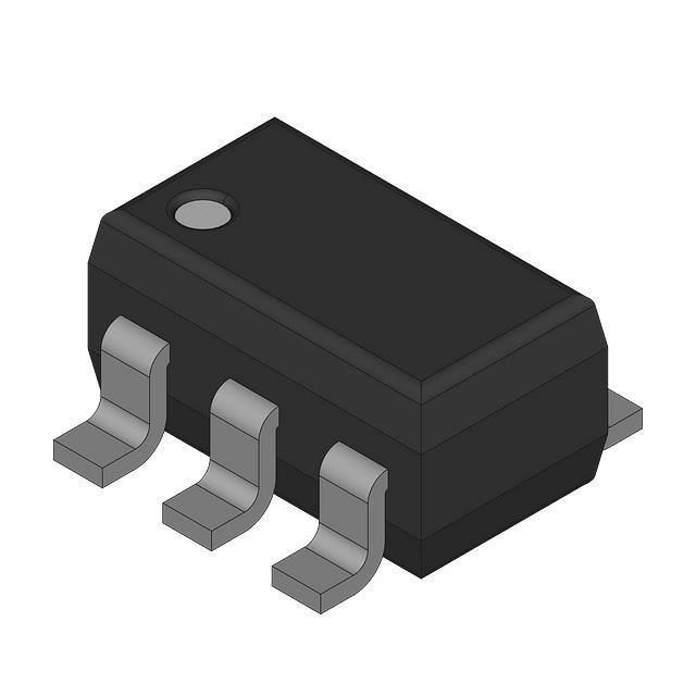
The NCP300 and NCP301 device series are available in the
Thin TSOP−5 package with standard undervoltage thresholds.
Additional thresholds that range from 0.9 V to 4.9 V in 100 mV steps
can be manufactured.
www.onsemi.com
MARKING DIAGRAM
TSOP−5/
SOT23−5
CASE 483
5
1
•
•
xxx AYWG
G
1
xxx
A
Y
W
G
Features
•
•
•
•
•
•
5
Quiescent Current of 0.5 mA Typical
High Accuracy Undervoltage Threshold of 2.0%
Wide Operating Voltage Range of 0.8 V to 10 V
Complementary or Open Drain Reset Output
Active Low or Active High Reset Output
Specified Over the −40°C to +125°C Temperature Range
(Except for Voltage Options from 0.9 to 1.1 V)
NCV Prefix for Automotive and Other Applications Requiring
Unique Site and Control Change Requirements; AEC−Q100
Qualified and PPAP Capable
These Devices are Pb−Free and are RoHS Compliant
= Specific Device Code
= Assembly Location
= Year
= Work Week
= Pb−Free Package
(Note:Microdot may be in either location)
PIN CONNECTIONS
Reset
Output
1
Input
2
Ground
3
5 N.C.
4 N.C.
(Top View)
ORDERING INFORMATION
Typical Applications
•
•
•
•
See detailed ordering and shipping information in the ordering
information section on page 21 of this data sheet.
Microprocessor Reset Controller
Low Battery Detection
Power Fail Indicator
Battery Backup Detection
NCP301xSNxxT1
Open Drain Output Configuration
NCP300xSNxxT1
Complementary Output Configuration
2
2
Input
1
Input
*
Vref
Reset Output
*
1
Reset Output
Vref
3
3
GND
GND
* The representative block diagrams depict active low reset output ‘L’ suffix devices. The comparator
inputs are interchanged for the active high output ‘H’ suffix devices.
This device contains 25 active transistors.
Figure 1. Representative Block Diagrams
© Semiconductor Components Industries, LLC, 2016
October, 2017 − Rev. 30
1
Publication Order Number:
NCP300/D
�NCP300, NCP301
MAXIMUM RATINGS
ÁÁÁÁÁÁÁÁÁÁÁÁÁÁÁÁÁÁÁÁÁÁÁÁÁÁÁÁÁÁÁÁÁÁÁÁ
ÁÁÁÁÁÁÁÁÁÁÁÁÁÁÁÁÁÁÁÁÁÁÁÁÁÁÁÁÁÁÁÁÁÁÁÁ
ÁÁÁÁÁÁÁÁÁÁÁÁÁÁÁÁÁÁÁÁÁÁÁÁÁÁÁÁÁÁÁÁÁÁÁÁ
ÁÁÁÁÁÁÁÁÁÁÁÁÁÁÁÁÁÁÁÁÁÁÁÁÁÁÁÁÁÁÁÁÁÁÁÁ
ÁÁÁÁÁÁÁÁÁÁÁÁÁÁÁÁÁÁÁÁÁÁÁÁÁÁÁÁÁÁÁÁÁÁÁÁ
ÁÁÁÁÁÁÁÁÁÁÁÁÁÁÁÁÁÁÁÁÁÁÁÁÁÁÁÁÁÁÁÁÁÁÁÁ
ÁÁÁÁÁÁÁÁÁÁÁÁÁÁÁÁÁÁÁÁÁÁÁÁÁÁÁÁÁÁÁÁÁÁÁÁ
ÁÁÁÁÁÁÁÁÁÁÁÁÁÁÁÁÁÁÁÁÁÁÁÁÁÁÁÁÁÁÁÁÁÁÁÁ
ÁÁÁÁÁÁÁÁÁÁÁÁÁÁÁÁÁÁÁÁÁÁÁÁÁÁÁÁÁÁÁÁÁÁÁÁ
ÁÁÁÁÁÁÁÁÁÁÁÁÁÁÁÁÁÁÁÁÁÁÁÁÁÁÁÁÁÁÁÁÁÁÁÁ
ÁÁÁÁÁÁÁÁÁÁÁÁÁÁÁÁÁÁÁÁÁÁÁÁÁÁÁÁÁÁÁÁÁÁÁÁ
ÁÁÁÁÁÁÁÁÁÁÁÁÁÁÁÁÁÁÁÁÁÁÁÁÁÁÁÁÁÁÁÁÁÁÁÁ
ÁÁÁÁÁÁÁÁÁÁÁÁÁÁÁÁÁÁÁÁÁÁÁÁÁÁÁÁÁÁÁÁÁÁÁÁ
Rating
Input Power Supply Voltage (Pin 2)
Symbol
Value
Unit
Vin
12
V
Output Voltage (Pin 1)
Complementary, NCP300
N−Channel Open Drain, NCP301
VOUT
V
Output Current (Pin 1) (Note 2)
IOUT
70
mA
Thermal Resistance Junction−to−Air
RqJA
250
°C/W
Maximum Junction Temperature
TJ
+150
°C
Operating Ambient Temperature Range
All Voltage Options: 0.9 V to 1.1 V
All Voltage Options: 1.2 V to 4.9 V
TA
TA
−40 to +85
−40 to +125
°C
°C
Storage Temperature Range
Tstg
−55 to +150
°C
Moisture Sensitivity Level
MSL
1
−0.3 to Vin +0.3
−0.3 to 12
Latchup Performance (Note 3)
Positive
Negative
ILATCHUP
mA
200
200
Stresses exceeding those listed in the Maximum Ratings table may damage the device. If any of these limits are exceeded, device functionality
should not be assumed, damage may occur and reliability may be affected.
1. This device series contains ESD protection and exceeds the following tests:
Human Body Model 2000 V per MIL−STD−883, Method 3015.
Machine Model Method 200 V.
2. The maximum package power dissipation limit must not be exceeded.
T
*T
J(max)
A
P +
D
R
qJA
3. Maximum ratings per JEDEC standard JESD78.
www.onsemi.com
2
�NCP300, NCP301
ELECTRICAL CHARACTERISTICS (For all values TA = −40°C to +125°C, unless otherwise noted.)
Characteristic
Symbol
Min
Typ
Max
Unit
NCP300/1 − 0.9 / NCV300/1 − 0.9 (TA = 255C for voltage options from 0.9 to 1.1 V)
Detector Threshold (Pin 2, Vin Decreasing)
VDET−
0.882
0.900
0.918
V
Detector Threshold Hysteresis (Pin 2, Vin Increasing)
VHYS
0.027
0.045
0.063
V
−
−
0.20
0.45
0.6
1.2
Supply Current (Pin 2)
(Vin = 0.8 V)
(Vin = 2.9 V)
mA
Iin
Maximum Operating Voltage (Pin 2)
Vin(max)
−
−
10
V
Minimum Operating Voltage (Pin 2)
(TA = −40°C to 85°C)
Vin(min)
−
−
0.55
0.65
0.70
0.80
V
Reset Output Current (Pin 1, Active Low ‘L’ Suffix Devices)
IOUT
mA
N−Channel Sink Current, NCP300, NCP301
(VOUT = 0.05 V, Vin = 0.70 V)
(VOUT = 0.50 V, Vin = 0.85 V)
0.01
0.05
0.05
0.50
−
−
P−Channel Source Current, NCP300
(VOUT = 2.4 V, Vin = 4.5 V)
1.0
6.0
−
Reset Output Current (Pin 1, Active High ‘H’ Suffix Devices)
IOUT
mA
N−Channel Sink Current, NCP300, NCP301
(VOUT = 0.5 V, Vin = 1.5 V)
1.05
2.5
−
P−Channel Source Current, NCP300
(VOUT = 0.4 V, Vin = 0.7 V)
(VOUT = GND, Vin = 0.8 V)
0.011
0.014
0.04
0.08
−
−
ms
Propagation Delay Input to Output (Figure 2)
Complementary Output NCP300 Series
Output Transition, High to Low
Output Transition, Low to High
tpHL
tpLH
−
−
97
77
−
300
N−Channel Open Drain NCP301 Series
Output Transition, High to Low
Output Transition, Low to High
tpHL
tpLH
−
−
97
−
−
300
Detector Threshold (Pin 2, Vin Decreasing) (TA = 25°C)
(TA = −40°C to 125°C)
VDET−
1.764
1.746
1.80
−
1.836
1.854
V
Detector Threshold Hysteresis (Pin 2, Vin Increasing)
VHYS
0.054
0.090
0.126
V
−
−
0.23
0.48
0.7
1.3
NCP300/1 − 1.8 / NCV300/1 − 1.8
Supply Current (Pin 2)
(Vin = 1.7 V)
(Vin = 3.8 V)
mA
Iin
Maximum Operating Voltage (Pin 2)
Vin(max)
−
−
10
V
Minimum Operating Voltage (Pin 2) (TA = 25°C)
(TA = −40°C to 125°C)
Vin(min)
−
−
0.55
0.65
0.70
0.80
V
Reset Output Current (Pin 1, Active Low ‘L’ Suffix Devices)
IOUT
mA
N−Channel Sink Current, NCP300, NCP301
(VOUT = 0.05V, Vin = 0.70 V)
(VOUT = 0.50V, Vin = 1.5 V)
0.01
1.0
0.05
2.0
−
−
P−Channel Source Current, NCP300
(VOUT = 2.4 V, Vin = 4.5 V)
1.0
6.0
−
Reset Output Current (Pin 1, Active High ‘H’ Suffix Devices)
IOUT
N−Channel Sink Current, NCP300, NCP301
(VOUT = 0.5 V, Vin = 5.0 V)
P−Channel Source Current, NCP300
(VOUT = 0.4 V, Vin = 0.7 V)
(VOUT = GND, Vin = 1.5 V)
mA
6.3
11
−
0.011
0.525
0.04
0.6
−
−
ms
Propagation Delay Input to Output (Figure 2)
Complementary Output NCP300 Series
Output Transition, High to Low
Output Transition, Low to High
tpHL
tpLH
www.onsemi.com
3
−
−
73
94
−
300
�NCP300, NCP301
ELECTRICAL CHARACTERISTICS (continued) (For all values TA = −40°C to +125°C, unless otherwise noted.)
Characteristic
Symbol
Min
Typ
Max
tpHL
tpLH
−
−
73
−
−
300
Detector Threshold (Pin 2, Vin Decreasing) (TA = 25°C)
(TA = −40°C to 125°C)
VDET−
1.96
1.94
2.00
−
2.04
2.06
Detector Threshold Hysteresis (Pin 2, Vin Increasing)
VHYS
0.06
0.10
0.14
Unit
NCP300/1 − 1.8 / NCV300/1 − 1.8
N−Channel Open Drain NCP301 Series
Output Transition, High to Low
Output Transition, Low to High
NCP300/1 − 2.0 / NCV300/1 − 2.0
Supply Current (Pin 2)
(Vin = 1.9 V)
(Vin = 4.0 V)
V
V
mA
Iin
−
−
0.23
0.48
0.8
1.3
Maximum Operating Voltage (Pin 2)
Vin(max)
−
−
10
V
Minimum Operating Voltage (Pin 2) (TA = 25°C)
(TA = −40°C to 125°C)
Vin(min)
−
−
0.55
0.65
0.70
0.80
V
Reset Output Current (Pin 1, Active Low ‘L’ Suffix Devices)
IOUT
mA
N−Channel Sink Current, NCP300, NCP301
(VOUT = 0.05V, Vin = 0.70V)
(VOUT = 0.50V, Vin = 1.5V)
0.01
1.0
0.14
3.5
−
−
P−Channel Source Current, NCP300
(VOUT = 2.4V, Vin = 4.5V)
1.0
9.7
−
Reset Output Current (Pin 1, Active High ‘H’ Suffix Devices)
IOUT
N−Channel Sink Current, NCP300, NCP301
(VOUT = 0.5 V, Vin = 5.0 V)
P−Channel Source Current, NCP300
(VOUT = 0.4 V, Vin = 0.7 V)
(VOUT = GND, Vin = 1.5 V)
mA
6.3
11
−
0.011
0.525
0.04
0.6
−
−
ms
Propagation Delay Input to Output (Figure 2)
Complementary Output NCP300 Series
Output Transition, High to Low
Output Transition, Low to High
tpHL
tpLH
−
−
55
108
−
300
N−Channel Open Drain NCP301 Series
Output Transition, High to Low
Output Transition, Low to High
tpHL
tpLH
−
−
55
−
−
300
Detector Threshold (Pin 2, Vin Decreasing) (TA = 25°C)
(TA = −40°C to 125°C)
VDET−
2.156
2.134
2.2
−
2.244
2.266
V
Detector Threshold Hysteresis (Pin 2, Vin Increasing)
VHYS
0.066
0.110
0.154
V
−
−
0.23
0.48
0.8
1.3
NCP300/1 − 2.2 / NCV300/1 − 2.2
Supply Current (Pin 2)
(Vin = 2.1 V)
(Vin = 4.2 V)
mA
Iin
Maximum Operating Voltage (Pin 2)
Vin(max)
−
−
10
V
Minimum Operating Voltage (Pin 2) (TA = 25°C)
(TA = −40°C to 125°C)
Vin(min)
−
−
0.55
0.65
0.70
0.80
V
Reset Output Current (Pin 1, Active Low ‘L’ Suffix Devices)
IOUT
mA
N−Channel Sink Current, NCP300, NCP301
(VOUT = 0.05V, Vin = 0.70V)
(VOUT = 0.50V, Vin = 1.5V)
0.01
1.0
0.14
3.5
−
−
P−Channel Source Current, NCP300
(VOUT = 2.4V, Vin = 4.5V)
1.0
9.7
−
Reset Output Current (Pin 1, Active High ‘H’ Suffix Devices)
IOUT
N−Channel Sink Current, NCP300, NCP301
(VOUT = 0.5 V, Vin = 5.0 V)
mA
6.3
www.onsemi.com
4
11
−
�NCP300, NCP301
ELECTRICAL CHARACTERISTICS (continued) (For all values TA = −40°C to +125°C, unless otherwise noted.)
Characteristic
Symbol
Min
Typ
Max
0.011
0.525
0.04
0.6
−
−
Unit
NCP300/1 − 2.2 / NCV300/1 − 2.2
P−Channel Source Current, NCP300
(VOUT = 0.4 V, Vin = 0.7 V)
(VOUT = GND, Vin = 1.5 V)
ms
Propagation Delay Input to Output (Figure 2)
Complementary Output NCP300 Series
Output Transition, High to Low
Output Transition, Low to High
tpHL
tpLH
−
−
55
108
−
300
N−Channel Open Drain NCP301 Series
Output Transition, High to Low
Output Transition, Low to High
tpHL
tpLH
−
−
55
−
−
300
Detector Threshold (Pin 2, Vin Decreasing) (TA = 25°C)
(TA = −40°C to 125°C)
VDET−
2.646
2.619
2.700
−
2.754
2.781
Detector Threshold Hysteresis (Pin 2, Vin Increasing)
VHYS
0.081
0.135
0.189
NCP300/1− 2.7 / NCV300/1− 2.7
Supply Current (Pin 2)
(Vin = 2.6 V)
(Vin = 4.7 V)
V
V
mA
Iin
−
−
0.25
0.50
0.8
1.3
Maximum Operating Voltage (Pin 2)
Vin(max)
−
−
10
V
Minimum Operating Voltage (Pin 2) (TA = 25°C)
(TA = −40°C to 125°C)
Vin(min)
−
−
0.55
0.65
0.70
0.80
V
Reset Output Current (Pin 1, Active Low ‘L’ Suffix Devices)
IOUT
mA
N−Channel Sink Current, NCP300, NCP301
(VOUT = 0.05V, Vin = 0.70V)
(VOUT = 0.50V, Vin = 1.5V)
0.01
1.0
0.14
3.5
−
−
P−Channel Source Current, NCP300
(VOUT = 2.4V, Vin = 4.5V)
1.0
9.7
−
Reset Output Current (Pin 1, Active High ‘H’ Suffix Devices)
IOUT
N−Channel Sink Current, NCP300, NCP301
(VOUT = 0.5 V, Vin = 5.0 V)
P−Channel Source Current, NCP300
(VOUT = 0.4 V, Vin = 0.7 V)
(VOUT = GND, Vin = 1.5 V)
mA
6.3
11
−
0.011
0.525
0.04
0.6
−
−
ms
Propagation Delay Input to Output (Figure 2)
Complementary Output NCP300 Series
Output Transition, High to Low
Output Transition, Low to High
tpHL
tpLH
−
−
55
115
−
300
N−Channel Open Drain NCP301 Series
Output Transition, High to Low
Output Transition, Low to High
tpHL
tpLH
−
−
55
−
−
300
Detector Threshold (Pin 2, Vin Decreasing) (TA = 25°C)
(TA = −40°C to 125°C)
VDET−
2.744
2.716
2.8
−
2.856
2.884
V
Detector Threshold Hysteresis (Pin 2, Vin Increasing)
VHYS
0.084
0.14
0.196
V
−
−
0.25
0.5
0.8
1.3
NCP300/1− 2.8 / NCV300/1− 2.8
Supply Current (Pin 2)
(Vin = 2.7 V)
(Vin = 4.8 V)
mA
Iin
Maximum Operating Voltage (Pin 2)
Vin(max)
−
−
10
V
Minimum Operating Voltage (Pin 2) (TA = 25°C)
(TA = −40°C to 125°C)
Vin(min)
−
−
0.55
0.65
0.7
0.8
V
Reset Output Current (Pin 1, Active Low ‘L’ Suffix Devices)
IOUT
N−Channel Sink Current, NCP300, NCP301
(VOUT = 0.05V, Vin = 0.70V)
(VOUT = 0.50V, Vin = 1.5V)
mA
0.01
1.0
www.onsemi.com
5
0.14
3.5
−
−
�NCP300, NCP301
ELECTRICAL CHARACTERISTICS (continued) (For all values TA = −40°C to +125°C, unless otherwise noted.)
Characteristic
Symbol
Min
Typ
Max
1.0
9.7
−
Unit
NCP300/1− 2.8 / NCV300/1− 2.8
P−Channel Source Current, NCP300
(VOUT = 2.4V, Vin = 4.5V)
Reset Output Current (Pin 1, Active High ‘H’ Suffix Devices)
IOUT
N−Channel Sink Current, NCP300, NCP301
(VOUT = 0.5 V, Vin = 5.0 V)
P−Channel Source Current, NCP300
(VOUT = 0.4 V, Vin = 0.7 V)
(VOUT = GND, Vin = 1.5 V)
mA
6.3
11
−
0.011
0.525
0.04
0.6
−
−
ms
Propagation Delay Input to Output (Figure 2)
Complementary Output NCP300 Series
Output Transition, High to Low
Output Transition, Low to High
tpHL
tpLH
−
−
55
115
−
300
N−Channel Open Drain NCP301 Series
Output Transition, High to Low
Output Transition, Low to High
tpHL
tpLH
−
−
55
−
−
300
Detector Threshold (Pin 2, Vin Decreasing) (TA = 25°C)
(TA = −40°C to 125°C)
VDET−
2.94
2.91
3.00
−
3.06
3.09
V
Detector Threshold Hysteresis (Pin 2, Vin Increasing)
VHYS
0.09
0.15
0.21
V
−
−
0.25
0.50
0.9
1.3
NCP300/1 − 3.0 / NCV300/1 − 3.0
Supply Current (Pin 2)
(Vin = 2.87 V)
(Vin = 5.0 V)
mA
Iin
Maximum Operating Voltage (Pin 2)
Vin(max)
−
−
10
V
Minimum Operating Voltage (Pin 2) (TA = 25°C)
(TA = −40°C to 125°C)
Vin(min)
−
−
0.55
0.65
0.70
0.80
V
Reset Output Current (Pin 1, Active Low ‘L’ Suffix Devices)
IOUT
mA
N−Channel Sink Current, NCP300, NCP301
(VOUT = 0.05V, Vin = 0.70V)
(VOUT = 0.50V, Vin = 1.5V)
0.01
1.0
0.14
3.5
−
−
P−Channel Source Current, NCP300
(VOUT = 2.4V, Vin = 4.5V)
1.0
9.7
−
Reset Output Current (Pin 1, Active High ‘H’ Suffix Devices)
IOUT
N−Channel Sink Current, NCP300, NCP301
(VOUT = 0.5 V, Vin = 5.0 V)
P−Channel Source Current, NCP300
(VOUT = 0.4 V, Vin = 0.7 V)
(VOUT = GND, Vin = 1.5 V)
mA
6.3
11
−
0.011
0.525
0.04
0.6
−
−
ms
Propagation Delay Input to Output (Figure 2)
Complementary Output NCP300 Series
Output Transition, High to Low
Output Transition, Low to High
tpHL
tpLH
−
−
49
115
−
300
N−Channel Open Drain NCP301 Series
Output Transition, High to Low
Output Transition, Low to High
tpHL
tpLH
−
−
49
−
−
300
Detector Threshold (Pin 2, Vin Decreasing) (TA = 25°C)
(TA = −40°C to 125°C)
VDET−
4.410
4.365
4.500
−
4.590
4.635
Detector Threshold Hysteresis (Pin 2, Vin Increasing)
VHYS
0.135
0.225
0.315
NCP300/1 − 4.5 / NCV300/1 − 4.5
Supply Current (Pin 2)
(Vin = 4.34 V)
(Vin = 6.5 V)
Vin(max)
www.onsemi.com
6
V
mA
Iin
Maximum Operating Voltage (Pin 2)
V
−
−
0.33
0.52
1.0
1.4
−
−
10
V
�NCP300, NCP301
ELECTRICAL CHARACTERISTICS (continued) (For all values TA = −40°C to +125°C, unless otherwise noted.)
Characteristic
Symbol
Min
Typ
Max
Unit
Vin(min)
−
−
0.55
0.65
0.70
0.80
V
NCP300/1 − 4.5 / NCV300/1 − 4.5
Minimum Operating Voltage (Pin 2) (TA = 25°C)
(TA = −40°C to 125°C)
Reset Output Current (Pin 1, Active Low ‘L’ Suffix Devices)
IOUT
N−Channel Sink Current, NCP300, NCP301
(VOUT = 0.05V, Vin = 0.70V)
(VOUT = 0.50V, Vin = 1.5V)
P−Channel Source Current, NCP300
(VOUT = 5.9V, Vin = 8.0V)
Reset Output Current (Pin 1, Active High ‘H’ Suffix Devices)
mA
0.01
1.0
0.05
2.0
−
−
1.5
10.5
−
IOUT
N−Channel Sink Current, NCP300, NCP301
(VOUT = 0.5 V, Vin = 5.0 V)
P−Channel Source Current, NCP300
(VOUT = 0.4 V, Vin = 0.7 V)
(VOUT = GND, Vin = 1.5 V)
mA
6.3
11
−
0.011
0.525
0.04
0.6
−
−
ms
Propagation Delay Input to Output (Figure 2)
Complementary Output NCP300 Series
Output Transition, High to Low
Output Transition, Low to High
tpHL
tpLH
−
−
49
130
−
300
N−Channel Open Drain NCP301 Series
Output Transition, High to Low
Output Transition, Low to High
tpHL
tpLH
−
−
49
−
−
300
Detector Threshold (Pin 2, Vin Decreasing) (TA = 25°C)
(TA = −40°C to 125°C)
VDET−
4.606
4.559
4.700
−
4.794
4.841
Detector Threshold Hysteresis (Pin 2, Vin Increasing)
VHYS
0.141
0.235
0.329
NCP300/1 − 4.7 / NCV300/1 − 4.7
Supply Current (Pin 2)
(Vin = 4.54 V)
(Vin = 6.7 V)
V
V
mA
Iin
−
−
0.34
0.53
1.0
1.4
Maximum Operating Voltage (Pin 2)
Vin(max)
−
−
10
V
Minimum Operating Voltage (Pin 2) (TA = 25°C)
(TA = −40°C to 125°C)
Vin(min)
−
−
0.55
0.65
0.70
0.80
V
Reset Output Current (Pin 1, Active Low ‘L’ Suffix Devices)
IOUT
mA
N−Channel Sink Current, NCP300, NCP301
(VOUT = 0.05V, Vin = 0.70V)
(VOUT = 0.50V, Vin = 1.5V)
0.01
1.0
0.05
2.0
−
−
P−Channel Source Current, NCP300
(VOUT = 5.9V, Vin = 8.0V)
1.5
10.5
−
Reset Output Current (Pin 1, Active High ‘H’ Suffix Devices)
IOUT
N−Channel Sink Current, NCP300, NCP301
(VOUT = 0.5 V, Vin = 5.0 V)
P−Channel Source Current, NCP300
(VOUT = 0.4 V, Vin = 0.7 V)
(VOUT = GND, Vin = 1.5 V)
mA
6.3
11
−
0.011
0.525
0.04
0.6
−
−
ms
Propagation Delay Input to Output (Figure 2)
Complementary Output NCP300 Series
Output Transition, High to Low
Output Transition, Low to High
tpHL
tpLH
−
−
45
130
−
300
N−Channel Open Drain NCP301 Series
Output Transition, High to Low
Output Transition, Low to High
tpHL
tpLH
−
−
45
−
−
300
Product parametric performance is indicated in the Electrical Characteristics for the listed test conditions, unless otherwise noted. Product
performance may not be indicated by the Electrical Characteristics if operated under different conditions.
www.onsemi.com
7
�NCP300, NCP301
VDET+ + 2
Input Voltage, Pin 2
0.7
0V
5V
Reset Output Voltage, Pin 1
2.5 V
NCP301L
Open Drain
0.5 V
0V
VDET+ + 2
Reset Output Voltage, Pin 1
VDET+ + 2
2
0V
NCP300L
Complementary
0.1 V
tpLH
tpHL
NCP300 and NCP301 series are measured with a 10 pF capacitive load. NCP301 has an additional 470 k pull−up resistor connected from the reset output to +5.0 V. The reset output voltage waveforms are shown for the active low ‘L’ devices. The upper detector
threshold, VDET+ is the sum of the lower detector threshold, VDET− plus the input hysteresis, VHYS.
Figure 2. Propagation Delay Measurement Conditions
www.onsemi.com
8
�NCP300, NCP301
Table 1. ELECTRICAL CHARACTERISTIC TABLE FOR 0.9 − 4.9 V
NCP300 Series
Supply Current
Nch Sink Current
Detector Threshold
Detector Threshold
Hysteresis
Vin Low
Vin High
Vin Low
Vin High
Pch Source
Current
VDET− (V) (Note 4)
VHYS (V)
Iin (mA)
(Note 5)
Iin (mA)
(Note 6)
IOUT (mA)
(Note 7)
IOUT (mA)
(Note 8)
IOUT (mA)
(Note 9)
Min
Typ
Max
Min
Typ
Max
Typ
Typ
Typ
Typ
Typ
NCP300LSN09T1
0.882
0.9
0.918
0.027
0.045
0.063
0.20
0.45
0.05
0.5
2.0
NCP300LSN18T1
1.764
1.8
1.836
0.054
0.090
0.126
0.23
0.48
NCP300LSN185T1
1.813
1.85
1.887
0.056
0.093
0.130
NCP300LSN20T1
1.960
2.0
2.040
0.060
0.100
0.140
NCP300LSN25T1
2.45
2.5
2.55
0.075
0.125
0.175
0.25
0.50
NCP300LSN27T1
2.646
2.7
2.754
0.081
0.135
0.189
0.25
0.50
NCP300LSN28T1
2.744
2.8
2.856
0.084
0.140
0.196
NCP300LSN30T1
2.940
3.0
3.060
0.090
0.150
0.210
NCP300LSN33T1
3.234
3.3
3.366
0.099
0.165
0.231
NCP300LSN34T1
3.332
3.4
3.468
0.102
0.170
0.238
NCP300LSN44T1
4.312
4.4
4.488
0.132
0.220
0.308
NCP300LSN45T1
4.410
4.5
4.590
0.135
0.225
0.315
0.33
0.52
NCP300LSN46T1
4.508
4.6
4.692
0.138
0.230
0.322
NCP300LSN47T1
4.606
4.7
4.794
0.141
0.235
0.329
0.34
0.53
Part Number
4. Values shown apply at +25°C only. For voltage options greater than 1.1 V, VDET− limits over operating temperature range (−40°C to +125°C)
are VNOM ±3%. For voltage options < 1.2 V, VDET− is guaranteed only at +25°C.
5. Condition 1: 0.9 − 2.9 V, Vin = VDET− − 0.10 V; 3.0 − 3.9 V, Vin = VDET− − 0.13 V; 4.0 − 4.9 V, Vin = VDET− − 0.16 V
6. Condition 2: 0.9 − 4.9 V, Vin = VDET− + 2.0 V
7. Condition 3: 0.9 − 4.9 V, Vin = 0.7 V, VOUT = 0.05 V, Active Low ‘L’ Suffix Devices
8. Condition 4: 0.9 − 1.0 V, Vin = 0.85 V, VOUT = 0.5 V; 1.1 − 1.5 V, Vin = 1.0 V, VOUT = 0.5 V; 1.6 − 4.9 V, Vin = 1.5 V, VOUT = 0.5 V,
Active Low ‘L’ Suffix Devices
9. Condition 5: 0.9 − 3.9 V, Vin = 4.5 V, VOUT = 2.4 V; 4.0 − 4.9 V, Vin = 8.0 V, VOUT = 5.9 V, Active Low ‘L’ Suffix Devices
Table 2. ELECTRICAL CHARACTERISTIC TABLE FOR 0.9 − 4.9 V
NCP300 Series
Supply Current
Pch Source Current
Detector Threshold
Detector Threshold
Hysteresis
Vin Low
Vin High
Nch Sink
Current
Vin Low
Vin High
VDET− (V) (Note 10)
VHYS (V)
Iin (mA)
(Note 11)
Iin (mA)
(Note 12)
IOUT (mA)
(Note 13)
IOUT (mA)
(Note 14)
IOUT (mA)
(Note 15)
Min
Typ
Max
Min
Typ
Max
Typ
Typ
Typ
Typ
Typ
NCP300HSN09T1
0.882
0.9
0.918
0.027
0.045
0.063
0.20
0.45
2.5
0.04
0.08
NCP300HSN18T1
1.764
1.8
1.836
0.054
0.090
0.126
0.23
0.48
NCP300HSN27T1
2.646
2.7
2.754
0.081
0.135
0.189
0.25
0.50
NCP300HSN30T1
2.940
3.0
3.060
0.090
0.150
0.210
NCP300HSN45T1
4.410
4.5
4.590
0.135
0.225
0.315
0.33
0.52
NCP300HSN47T1
4.606
4.7
4.794
0.141
0.235
0.329
0.34
0.53
Part Number
10. Values shown apply at +25°C only. For voltage options greater than 1.1 V, VDET− limits over operating temperature range (−40°C to +125°C)
are VNOM ±3%. For voltage options < 1.2 V, VDET− is guaranteed only at +25°C.
11. Condition 1: 0.9 − 2.9 V, Vin = VDET− − 0.10 V; 3.0 − 3.9 V, Vin = VDET− − 0.13 V; 4.0 − 4.9 V, Vin = VDET− − 0.16 V
12. Condition 2: 0.9 − 4.9 V, Vin = VDET− + 2.0 V
13. Condition 3: 0.9 − 1.4 V, Vin = 1.5 V, VOUT = 0.5 V; 1.5 − 4.9 V, Vin = 5.0 V, VOUT = 0.5 V, Active High ‘H’ Suffix Devices
14. Condition 4: 0.9 − 4.9 V, Vin = 0.7 V, VOUT = 0.4 V, Active High ‘H’ Suffix Devices
15. Condition 5: 0.9 − 1.0 V, Vin = 0.8 V, VOUT = GND; 1.1 − 1.5 V, Vin = 1.0 V, VOUT = GND; 1.6 − 4.9 V, Vin = 1.5 V, VOUT = GND,
Active High ‘H’ Suffix Devices
www.onsemi.com
9
�NCP300, NCP301
Table 3. ELECTRICAL CHARACTERISTIC TABLE FOR 0.9 − 4.9 V
NCP301 Series
Supply Current
Nch Sink Current
Detector Threshold
Detector Threshold
Hysteresis
Vin Low
Vin High
Vin Low
Vin High
VDET− (V) (Note 16)
VHYS (V)
Iin (mA)
(Note 16)
Iin (mA)
(Note 18)
IOUT (mA)
(Note 19)
IOUT (mA)
(Note 20)
Min
Typ
Max
Min
Typ
Max
Typ
Typ
Typ
Typ
NCP301LSN09T1
0.882
0.9
0.918
0.027
0.045
0.063
0.20
0.45
0.05
0.5
NCP301LSN12T1
1.176
1.2
1.224
0.036
0.060
0.084
NCP301LSN16T1
1.568
1.6
1.632
0.048
0.080
0.112
NCP301LSN18T1
1.764
1.8
1.836
0.054
0.090
0.126
0.23
0.48
NCP301LSN20T1
1.960
2.0
2.040
0.060
0.100
0.140
NCP301LSN22T1
2.156
2.2
2.244
0.066
0.110
0.154
NCP301LSN24T1
2.352
2.4
2.448
0.072
0.120
0.168
NCP301LSN25T1
2.450
2.5
2.550
0.075
0.125
0.175
NCP301LSN26T1
2.548
2.6
2.652
0.078
0.130
0.182
NCP301LSN27T1
2.646
2.7
2.754
0.081
0.135
0.189
0.25
0.50
NCP301LSN28T1
2.744
2.8
2.856
0.084
0.140
0.196
NCP301LSN30T1
2.940
3.0
3.060
0.090
0.150
0.210
NCP301LSN31T1
3.038
3.1
3.162
0.093
0.155
0.217
NCP301LSN32T1
3.136
3.2
3.264
0.096
0.160
0.224
NCP301LSN33T1
3.234
3.3
3.366
0.099
0.165
0.231
NCP301LSN34T1
3.332
3.4
3.468
0.102
0.170
0.238
NCP301LSN36T1
3.528
3.6
3.672
0.108
0.180
0.252
NCP301LSN40T1
3.920
4.0
4.080
0.120
0.200
0.280
NCP301LSN42T1
4.116
4.2
4.284
0.126
0.210
0.294
NCP301LSN45T1
4.410
4.5
4.590
0.135
0.225
0.315
0.33
0.52
NCP301LSN46T1
4.508
4.6
4.692
0.138
0.230
0.322
NCP301LSN47T1
4.606
4.7
4.794
0.141
0.235
0.329
0.34
0.53
Part Number
2.0
16. Values shown apply at +25°C only. For voltage options greater than 1.1 V, VDET− limits over operating temperature range (−40°C to +125°C)
are VNOM ±3%. For voltage options < 1.2 V, VDET− is guaranteed only at +25°C.
17. Condition 1: 0.9 − 2.9 V, Vin = VDET− − 0.10 V; 3.0 − 3.9 V, Vin = VDET− − 0.13 V; 4.0 − 4.9 V, Vin = VDET− − 0.16 V
18. Condition 2: 0.9 − 4.9 V, Vin = VDET− + 2.0 V
19. Condition 3: 0.9 − 4.9 V, Vin = 0.7 V, VOUT = 0.05 V, Active Low ‘L’ Suffix Devices
20. Condition 4: 0.9 − 1.0 V, Vin = 0.85 V, VOUT = 0.5 V; 1.1 − 1.5 V, Vin = 1.0 V, VOUT = 0.5 V; 1.6 − 4.9 V, Vin = 1.5 V, VOUT = 0.5 V,
Condition 4: Active Low ‘L’ Suffix Devices
Table 4. ELECTRICAL CHARACTERISTIC TABLE FOR 0.9 − 4.9 V
NCP301 Series
Supply Current
Detector Threshold
Detector Threshold
Hysteresis
Vin Low
Vin High
Nch
Sink Current
VDET− (V) (Note 21)
VHYS (V)
Iin (mA)
(Note 22)
Iin (mA)
(Note 23)
IOUT (mA)
(Note 24)
Min
Typ
Max
Min
Typ
Max
Typ
Typ
Typ
NCP301HSN09T1
0.882
0.9
0.918
0.027
0.045
0.063
0.20
0.45
2.5
NCP301HSN18T1
1.764
1.8
1.836
0.054
0.090
0.126
NCP301HSN22T1
2.156
2.2
2.244
0.066
0.110
0.154
NCP301HSN27T1
2.646
2.7
2.754
0.081
0.135
0.189
0.25
0.50
NCP301HSN30T1
2.940
3.0
3.060
0.090
0.150
0.210
NCP301HSN45T1
4.410
4.5
4.590
0.135
0.225
0.315
0.33
0.52
Part Number
21. Values shown apply at +25°C only. For voltage options greater than 1.1 V, VDET− limits over operating temperature range (−40°C to
+125°C) are VNOM ±3%. For voltage options < 1.2 V, VDET− is guaranteed only at +25°C.
22. Condition 1: 0.9 − 2.9 V, Vin = VDET− − 0.10 V; 3.0 − 3.9 V, Vin = VDET− − 0.13 V; 4.0 − 4.9 V, Vin = VDET− − 0.16 V
23. Condition 2: 0.9 − 4.9 V, Vin = VDET− + 2.0 V
24. Condition 3: 0.9 − 1.4 V, Vin = 1.5 V, VOUT = 0.5 V; 1.5 − 4.9 V, Vin = 5.0 V, VOUT = 0.5 V, Active High ‘H’ Suffix Devices
www.onsemi.com
10
�NCP300, NCP301
1.0
10.5
0.9
0.8
Iin, INPUT CURRENT (mA)
Iin, INPUT CURRENT (mA)
TA = 25°C
TA = 25°C
0.7
0.6
0.5
0.4
0.3
0.2
2.5
2.0
1.5
1.0
0.5
0.1
0
0
0
2.0
4.0
6.0
8.0
10
12
0
6.0
4.0
8.0
Vin, INPUT VOLTAGE (V)
2.0
Vin, INPUT VOLTAGE (V)
Figure 3. NCP300/1 Series 0.9 V
Input Current versus Input Voltage
VDET, DETECTOR THRESHOLD VOLTAGE (V)
Iin, INPUT CURRENT (mA)
TA = 25°C
2.5
2.0
1.5
1.0
0.5
0
2.0
4.0
8.0
6.0
10
12
Vin, INPUT VOLTAGE (V)
1.00
0.95
VDET−
0.85
0.80
−50
VDET+
2.75
2.70
VDET−
−25
0
25
50
75
100
125
TA, AMBIENT TEMPERATURE (°C)
VDET, DETECTOR THRESHOLD VOLTAGE (V)
VDET, DETECTOR THRESHOLD VOLTAGE (V)
2.85
2.60
−50
0
−25
25
50
75
100
TA, AMBIENT TEMPERATURE (°C)
Figure 6. NCP300/1 Series 0.9 V
Detector Threshold Voltage versus Temperature
2.90
2.65
VDET+
0.90
Figure 5. NCP300/1 Series 4.5 V
Input Current versus Input Voltage
2.80
12
Figure 4. NCP300/1 Series 2.7 V
Input Current versus Input Voltage
17.2
0
10
4.9
4.8
VDET+
4.7
4.6
4.5
VDET−
4.4
4.3
−50
−25
0
25
50
75
100
125
TA, AMBIENT TEMPERATURE (°C)
Figure 8. NCP300/1 Series 4.5 V
Detector Threshold Voltage versus Temperature
Figure 7. NCP300/1 Series 2.7 V
Detector Threshold Voltage versus Temperature
www.onsemi.com
11
�NCP300, NCP301
3.5
VOUT, OUTPUT VOLTAGE (V)
VOUT, OUTPUT VOLTAGE (V)
1.0
0.8
0.6
TA = −40°C (301L only)
0.4
TA = 25°C (301L only)
0.2
3.0
2.5
2.0
1.5
TA = 125°C (301L only)
1.0
TA = −40°C (301L only)
0.5
TA = 25°C (301L only)
0
0
0
0.4
0.6
Vin, INPUT VOLTAGE (V)
0.2
1.0
0.8
0
Figure 9. NCP300L/1L Series 0.9 V
Reset Output Voltage versus Input Voltage
1.6
IOUT, OUTPUT SINK CURRENT (mA)
VOUT, OUTPUT VOLTAGE (V)
3.5
Figure 10. NCP300L/1L Series 2.7 V
Reset Output Voltage versus Input Voltage
6.0
5.0
4.0
3.0
TA = −40°C (301L only)
2.0
TA = 25°C (301L only)
1.0
0
VOUT = 0.5 V
1.4
TA = −40°C
1.2
1.0
0.8
0.6
TA = 25°C
0.4
TA = 85°C
0.2
0
0
1.0
2.0
4.0
3.0
Vin, INPUT VOLTAGE (V)
5.0
6.0
0
0.4
0.2
0.6
0.8
1.0
Vin, INPUT VOLTAGE (V)
Figure 11. NCP300L/1L Series 4.5 V
Reset Output Voltage versus Input Voltage
Figure 12. NCP300H/1L Series 0.9 V
Reset Output Sink Current versus Input Voltage
12
20
VOUT = 0.5 V
IOUT, OUTPUT SINK CURRENT (mA)
IOUT, OUTPUT SINK CURRENT (mA)
3.0
1.5
2.5
1.0
2.0
Vin, INPUT VOLTAGE (V)
0.5
10
TA = −40°C
8.0
6.0
TA = 25°C
4.0
TA = 125°C
2.0
0
0
0.5
1.0
1.5
2.0
2.5
3.0
VOUT = 0.5 V
TA = −40°C
15
10
TA = 25°C
TA = 125°C
5.0
0
0
1.0
2.0
3.0
4.0
5.0
Vin, INPUT VOLTAGE (V)
Vin, INPUT VOLTAGE (V)
Figure 13. NCP300H/1L Series 2.7 V
Reset Output Sink Current versus Input Voltage
Figure 14. NCP300H/1L Series 4.5 V
Reset Output Sink Current versus Input Voltage
www.onsemi.com
12
�20
IOUT, OUTPUT SOURCE CURRENT (mA)
IOUT, OUTPUT SOURCE CURRENT (mA)
NCP300, NCP301
VOUT = Vin −2.1 V
TA = 25°C
15
Vin −1.5 V
10
Vin −1.0 V
5.0
Vin −0.5 V
0
0
2.0
4.0
8.0
6.0
10
20
VOUT = Vin −2.1 V
TA = 25°C
15
Vin −1.5 V
Vin −1.0 V
10
Vin −0.5 V
5.0
0
0
4.0
2.0
20
VOUT = Vin −2.1 V
15
Vin −1.5 V
10
Vin −1.0 V
5.0
Vin −0.5 V
0
0
2.0
4.0
8.0
6.0
1.5
TA = 25°C
1.0
Vin = 0.85 V
0.5
Vin = 0.7 V
0
10
0
0.4
0.2
Vin, INPUT VOLTAGE (V)
0.6
0.8
1.0
VOUT, OUTPUT VOLTAGE (V)
Figure 17. NCP300L Series 4.5 V
Reset Output Source Current versus Input Voltage
Figure 18. NCP300H/1L Series 0.9 V
Reset Output Sink Current versus Output Voltage
15
35
TA = 25°C
IOUT, OUTPUT SINK CURRENT (mA)
IOUT, OUTPUT SINK CURRENT (mA)
10
Figure 16. NCP300L Series 2.7 V
Reset Output Source Current versus Input Voltage
IOUT, OUTPUT SINK CURRENT (mA)
IOUT, OUTPUT SOURCE CURRENT (mA)
Figure 15. NCP300L Series 0.9 V
Reset Output Source Current versus Input Voltage
TA = 25°C
8.0
6.0
Vin, INPUT VOLTAGE (V)
Vin, INPUT VOLTAGE (V)
Vin = 2.5 V
10
Vin = 2.0 V
5.0
Vin = 1.5 V
0
TA = 25°C
30
Vin = 4.0 V
25
Vin = 3.5 V
20
Vin = 3.0 V
15
Vin = 2.5 V
10
Vin = 2.0 V
5.0
Vin = 1.5 V
0
0
0.5
1.0
1.5
2.0
0
2.5
1.0
2.0
3.0
4.0
VOUT, OUTPUT VOLTAGE (V)
VOUT, OUTPUT VOLTAGE (V)
Figure 19. NCP300H/1L Series 2.7 V
Reset Output Sink Current versus Output Voltage
Figure 20. NCP300H/1L Series 4.5 V
Reset Output Sink Current versus Output Voltage
www.onsemi.com
13
�NCP300, NCP301
OPERATING DESCRIPTION
The NCP300 and NCP301 series devices are second
generation ultra−low current voltage detectors. Figures 20
and 21 show a timing diagram and a typical application.
Initially consider that input voltage Vin is at a nominal level
and it is greater than the voltage detector upper threshold
(VDET+), and the reset output (Pin 1) will be in the high state
for active low devices, or in the low state for active high
devices. If there is a power interruption and Vin becomes
significantly deficient, it will fall below the lower detector
threshold (VDET−). This sequence of events causes the Reset
output to be in the low state for active low devices, or in the
Input Voltage, Pin 2
Reset Output (Active Low), Pin 1
high state for active high devices. After completion of the
power interruption, Vin will again return to its nominal level
and become greater than the VDET+. The voltage detector
has built−in hysteresis to prevent erratic reset operation as
the comparator threshold is crossed.
Although these device series are specifically designed for
use as reset controllers in portable microprocessor based
systems, they offer a cost−effective solution in numerous
applications where precise voltage monitoring is required.
Figure 26 through Figure 33 shows various application
examples.
Vin
VDET+
VDET−
Vin
VDET+
VDET−
0V
Reset Output (Active High), Pin 1
Vin
VDET+
VDET−
0V
Figure 21. Timing Waveforms
www.onsemi.com
14
�NCP300, NCP301
VCC TRANSIENT REJECTION
The NCP300 and NCP301 series provides accurate VCC
monitoring and reset timing during power−up,
power−down, and brownout/sag conditions, and rejects
negative glitches on the power supply line. Figure 22 shows
the maximum transient duration vs. maximum negative
excursion (overdrive) for glitch rejection. Any combination
of duration and overdrive which lies under the curve will not
generate a reset signal. A below−VCC condition (on the
right) is detected as a brownout or power−down. Typically,
any transient that goes 100 mV below the reset threshold and
lasts 5.0 ms or less will not cause a reset pulse.
Transient immunity can be improved by adding a
capacitor in close proximity to the VCC pin of the NCP30x.
FACTORS TO BE CONSIDERED FOR VOLTAGE
OPTION SELECTION
The following hysteresis graph depicts VDET−_min/max
and VDET+_min/max for an active low Reset device:
Output
VDET−_typ
VDET−_min
VDET−_max
VDET+_min
VDET+_max
Input
VCC
VDET+_min = VDET−_min + VHYS_min
VDET+_max = VDET−_max + VHYS_max
VTH
Overdrive
Figure 24.
For selecting a voltage option in the NCP30X family,
three major factors should be considered:
1. VDET+_max: Maximum detector threshold voltage
for increasing Vin for the NCP30X device.
2. Vin_min: Minimum voltage output of the power
supply. This is also the input voltage to the
NCP30X device.
3. VCC_min: Minimum power supply voltage
specification for the device that is protected by the
NCP30X.
The VDET+_max for an NCP30X device is normally
calculated as follows:
Duration
Figure 22. Max Transient Duration vs. Max Overdrive
300
TRANSIENT DURATION
250
200
VTH = 4.90 V
150
V DET+_max + V DET−_max ) V HYS_max
VTH = 3.10 V
100
VTH = 1.60 V
Where:
VDET−_max = Maximum detector threshold voltage for
decreasing Vin
VHYS_max = Maximum detector threshold hysteresis
The above two parameters can be obtained directly from
the data sheet to figure out the VDET+_max.
In the NCP30X family, for a given VDET−_typ, which is the
typical detection voltage reflected in the part number, the
threshold values are designed to the following targets (at
25°C):
50
0
10
30
50
70
90
110
130
RESET COMPARATOR OVERDRIVE
(eq. 1)
150
Figure 23.
V DET−_min + V DET−_typ * 2%
(eq. 2)
V DET−_max + V DET−_typ ) 2%
(eq. 3)
V HYS_typ + 5% of V DET−_typ
(eq. 4)
V HYS_min + V HYS_typ * 40%
(eq. 5)
V HYS_max + V HYS_typ ) 40%
(eq. 6)
By simple mathematical calculation,
Equations 2 to 6, Equation 1 becomes:
V DET+_max + V DET−_typ
www.onsemi.com
15
1.09
combining
(eq. 7)
�NCP300, NCP301
PROPAGATION DELAY VARIATION
On the other hand (see above paragraph), a minimum
overdrive value from Vthreshold to VCC must be respected.
That means Vin (minimum value of VCC) must be higher
enough than VDET+ (VDET− + hysteresis) at the risk of
significantly increasing propagation delay. (Figure 25) This
propagation delay is temperature sensitive.
To avoid acceptable time response, a minimum 100 mV
difference between Vin and VDET+ must be selected.
So, VDET+_max can be easily figured out just using a single
variable VDET−_typ.
For example, for NCP300LSN18T1G VDET−_typ = 1.8 V;
then
V DET+_max + 1.8
1.09 + 1.962 V
(eq. 8)
The NCP30X detection voltage option must be chosen such
that:
V CC_min t V DET+_max t V in_min
(eq. 9)
The significance of VCC_min < VDET+_max is that it makes
sure the the reset from NCP30X remains asserted (in RESET
hold state) till after the power supply exceeds the VCC_min
requirement; this prevents incorrect device (uP) initiation.
Having VDET+_max < Vin_min makes sure that the
NCP30X is able to start up when Vin is at the Vin_min.
The theoretical ideal VDET−_typ voltage option to be
selected by the user, VDET−_typ_ideal, can be given by the
following formula:
V DET−_typ_ideal +
(2
600
500
TIME DELAY (ms)
ǒVin_min ) VCC_minǓ
VDET+
400
300
tpLH
200
(eq. 10)
tpHL
1.09)
100
The following example shows how to select the device
voltage option in a real world application.
1. Power supply output specification: 3.3 V $3%
2. Microprocessor core voltage specification: 3.3 V
$5%
So, we have:
V in_min + 3.3 V * 3% + 3.201 V
(eq. 11)
V CC_min + 3.3 V * 5% + 3.135 V
(eq. 12)
0
3.0
3.168
3.5
4.0
4.5
5.0
Vin, PULSE HIGH INPUT VOLTAGE (V)
Figure 25. tpLH and tpHL vs. Input Voltage
for the NCP301SNT1
Then the ideal voltage option = (3.201 + 3.135) / (2 * 1.09)
= 2.9064 V
Therefore, a device voltage option of 2.9 V will be the right
choice.
www.onsemi.com
16
5.5
�NCP300, NCP301
APPLICATION CIRCUIT INFORMATION
VDD
VDD
2
Input
NCP300
Series
3
*
1
Microprocessor
Reset
Reset Output
* Required for
GND
GND
NCP301
Figure 26. Microprocessor Reset Circuit
2.85 V
2.70 V
Vin < 2.7 ON
2
Input
NCP300
LSN27T1
1
To Additional Circuitry
Reset Output
Vin > 2.835 ON
3
GND
Figure 27. Battery Charge Indicator
Vsupply
Fault
10 V
Active High
Device Thresholds
2
UV
NCP301
LSN23T1
Active Low
Device Thresholds
1.0 V
Input
UV
Fault
OK
OV
Fault
OV
Fault
OK
UV
Fault
3
GND
2
Input
1
Reset Output
Input
The above circuit combines an active high and an active low reset output device to form
a window detector for monitoring battery or power supply voltages. When the input
voltage falls outside of the window established by the upper and lower device
thresholds, the LED will turn on indicating a fault. As the input voltage falls within the
window, increasing from 1.0 V and exceeding the active low device’s hysteresis
threshold, or decreasing from the peak towards 1.0 V and falling below the active high
device’s undervoltage threshold, the LED will turn off. The device thresholds shown can
be used for a single cell lithium−ion battery charge detector.
Figure 28. Window Voltage Detector
www.onsemi.com
17
OV
NCP301
HSN43T1
3
GND
1
Reset Output
Output
�NCP300, NCP301
APPLICATION CIRCUIT INFORMATION
Vsupply
5.0 V
2
Input
1
NCP301
LSN45T1
Reset Output
3
GND
2
Input
3.3 V
1
NCP301
LSN30T1
Low state output if either power
supply is below the respective
undervoltage detector threshold
but greater than 1.0 V.
Reset Output
GND
3
Figure 29. Dual Power Supply Undervoltage Supervision
VDD
RH
2
VDD
Input
RL
NCP301
LSN27T1
3
1
Microprocessor
Reset
Reset Output
GND
GND
Figure 30. Microprocessor Reset Circuit with Additional Hysteresis
Comparator hysteresis can be increased with the addition of
resistor RH. The hysteresis equations have been simplified and
do not account for the change of input current Iin as Vin crosses
the comparator threshold. The internal resistance, Rin is simply
calculated using Iin = 0.26 mA at 2.6 V.
Vin Decreasing:
V th +
Vin Increasing:
V th +
ǒ
ǒRR
H
Ǔ
) 1 ǒV DET*Ǔ
in
Ǔ
RH
) 1 ǒV DET* ) V HYSǓ
R in ø R L
VHYS = Vin Increasing − Vin Decreasing
Test Data
ÁÁÁÁÁÁÁÁÁÁÁÁÁÁÁÁÁÁÁÁ
ÁÁÁÁÁÁÁÁÁÁÁÁÁÁÁÁÁÁÁÁ
ÁÁÁÁÁÁÁÁÁÁÁÁÁÁÁÁÁÁÁÁ
ÁÁÁÁÁÁÁÁÁÁÁÁÁÁÁÁÁÁÁÁ
ÁÁÁÁÁÁ
ÁÁÁÁÁÁÁÁÁÁÁÁ
ÁÁÁÁÁÁÁÁÁ
ÁÁÁÁÁÁ
ÁÁÁÁÁ
ÁÁ
ÁÁÁÁÁÁÁÁÁÁÁÁÁÁÁÁÁÁÁÁ
ÁÁÁÁÁÁÁÁÁÁÁÁÁÁÁÁÁÁÁÁ
Vth Decreasing
(V)
Vth Increasing
(V)
VHYS
(V)
RH
(W)
RL
(kW)
2.70
2.70
2.70
2.70
2.70
2.70
2.70
2.70
2.70
2.70
2.84
2.87
2.88
2.91
2.90
2.94
2.98
2.97
3.04
3.15
0.135
0.17
0.18
0.21
0.20
0.24
0.28
0.27
0.34
0.45
0
100
100
100
220
220
220
470
470
470
−
10
6.8
4.3
10
6.8
4.3
10
6.8
4.3
www.onsemi.com
18
�NCP300, NCP301
5.0 V
Test Data
R2 = 82 kW
R1 = 100 kW
Input
2
R2 (See table)
C
NCP301
NCP300
HSN27T1
LSN27T1
fOSC (kHz)
IQ (mA)
fOSC (kHz)
IQ (mA)
0.01
10.4
18
6.0
30
0.068
9.8
18
5.7
30
1.0
6.18
21
3.6
29
1
10
1.41
21
1.34
25
Reset Output
100
0.27
22
0.356
23
1000
0.045
22
0.077
22
GND
3
R2 = 8.2 kW
C (nF)
Table values are for information only.
Figure 31. Simple Clock Oscillator
Vsupply
This circuit monitors the current at the load. As
current flows through the load, a voltage drop with
respect to ground appears across Rsense where
Vsense = Iload * Rsense. The following conditions apply:
Load
VDD
Rsense
2
If:
ILoad t VDET − /Rsense
ILoad w (VDET −+VHYS)/Rsense
Input
50 k
NCP301
LSN09T1
LSN27T1
3
GND
1
Microcontroller
Reset Output
GND
Figure 32. Microcontroller System Load Sensing
www.onsemi.com
19
Then:
Reset Output = 0 V
Reset Output = VDD
�NCP300, NCP301
Vsupply
2
Input
NCP301
LSN27T1
LSN45T1
3
GND
2
Input
NCP301
LSN27T1
3
GND
2
Input
1
Reset
Output
1
Reset
Output
Vin = 1.0 V to 10 V
NCP301
LSN27T1
LSN18T1
3
1
Reset
Output
GND
A simple voltage monitor can be constructed by connecting several voltage detectors as shown above. Each LED will
sequentially turn on when the respective voltage detector threshold (VDET− +VHYS) is exceeded. Note that detector
thresholds (VDET−) that range from 0.9 V to 4.9 V in 100 mV steps can be manufactured.
Figure 33. LED Bar Graph Voltage Monitor
www.onsemi.com
20
�NCP300, NCP301
ORDERING INFORMATION
Device
Threshold Voltage
NCP300LSN09T1G
Output Type
Reset
Marking
Package
0.9
SEJ
TSOP−5
(Pb−Free)
NCP300LSN18T1G
1.8
SFK
TSOP−5
(Pb−Free)
NCP300LSN185T1G
1.85
SRA
TSOP−5
(Pb−Free)
NCP300LSN20T1G
NCV300LSN20T1G*
NCP300LSN25T1G
2.0
SHE
SIM
TSOP−5
(Pb−Free)
RUM
TSOP−5
(Pb−Free)
NCP300LSN27T1G
NCV300LSN27T1G*
NCP300LSN28T1G
NCV300LSN28T1G*
NCP300LSN30T1G
NCV300LSN30T1G*
NCP300LSN33T1G
2.7
2.5
TSOP−5
(Pb−Free)
3.3
SEE
SIW
SED
SSL
SEC
SQV
SKV
NCP300LSN34T1G
NCV300LSN36T1G*
NCP300LSN44T1G
3.4
3.6
4.4
SKU
SKS
SKK
TSOP−5
(Pb−Free)
NCP300LSN45T1G
4.5
SEA
TSOP−5
(Pb−Free)
NCP300LSN46T1G
4.6
SKJ
TSOP−5
(Pb−Free)
NCP300LSN47T1G
4.7
SDZ
TSOP−5
(Pb−Free)
NCP300HSN09T1G
0.9
SDY
TSOP−5
(Pb−Free)
NCP300HSN18T1G
1.8
SFJ
TSOP−5
(Pb−Free)
NCP300HSN27T1G
2.7
SDU
TSOP−5
(Pb−Free)
SDS
TSOP−5
(Pb−Free)
2.8
3.0
Active
Low
CMOS
Active
High
CMOS
TSOP−5
(Pb−Free)
TSOP−5
(Pb−Free)
3000 / Tape & Reel
(7 in. Reel)
TSOP−5
(Pb−Free)
TSOP−5
(Pb−Free)
NCP300HSN30T1G
3.0
NCP300HSN45T1G
4.5
SDQ
TSOP−5
(Pb−Free)
NCP300HSN47T1G
4.7
SDP
TSOP−5
(Pb−Free)
NOTE:
Shipping†
3000 / Tape & Reel
(7 in. Reel)
The ordering information lists standard undervoltage thresholds with active low outputs. Additional active low threshold devices,
ranging from 0.9 V to 4.9 V in 100 mV increments and NCP300/NCP301 active high output devices, ranging from 0.9 V to 4.9 V
in 100 mV increments can be manufactured. Contact your ON Semiconductor representative for availability. The electrical
characteristics of these additional devices are shown in Tables 1 through 4.
†For information on tape and reel specifications, including part orientation and tape sizes, please refer to our Tape and Reel Packaging Specifications Brochure, BRD8011/D.
*NCV prefix for Automotive and Other Applications Requiring Unique Site and Control Change Requirements; AEC−Q100 Qualified and PPAP
Capable.
NCVxxx: Tlow = −40°C, Thigh = +125°C. Guaranteed by design.
www.onsemi.com
21
�NCP300, NCP301
ORDERING INFORMATION
Device
Threshold Voltage
NCP301LSN09T1G
NCP301LSN12T1G
Output Type
Reset
Marking
Package
0.9
SFF
TSOP−5
(Pb−Free)
1.2
SNN
TSOP−5
(Pb−Free)
SRK
TSOP−5
TSOP−5
(Pb−Free)
SNJ
TSOP−5
(Pb−Free)
SRL
TSOP−5
TSOP−5
(Pb−Free)
SFN
TSOP−5
(Pb−Free)
DT2
TSOP−5
(Pb−Free)
SFD
SRM
SNG
TSOP−5
(Pb−Free)
SUA
TSOP−5
TSOP−5
(Pb−Free)
TAN
TSOP−5
(Pb−Free)
SNF
TSOP−5
(Pb−Free)
NCP301LSN25T2G
ET2
TSOP−5
(Pb−Free)
NCV301LSN25T1G*
SRN
TSOP−5
(Pb−Free)
NCV301LSN12T1*
NCV301LSN12T1G*
NCP301LSN16T1G
1.6
NCV301LSN16T1*
NCV301LSN16T1G*
NCP301LSN18T1G
1.8
NCP301LSN18T2G
NCP301LSN20T1G
NCV301LSN20T1G*
NCP301LSN22T1G
2.0
2.2
NCV301LSN22T1*
NCV301LSN22T1G*
NCP301LSN24T1G
NCP301LSN25T1G
2.4
2.5
Open
Drain
Active
Low
TSOP−5
(Pb−Free)
NCP301LSN26T1G
2.6
SNE
TSOP−5
(Pb−Free)
NCP301LSN27T1G
2.7
SFA
TSOP−5
(Pb−Free)
FT2
TSOP−5
(Pb−Free)
SEZ
TSOP−5
(Pb−Free)
SRO
TSOP−5
(Pb−Free)
SEY
TSOP−5
(Pb−Free)
NCP301LSN30T2G
GT2
TSOP−5
(Pb−Free)
NCV301LSN30T1G*
AJA
TSOP−5
(Pb−Free)
NCP301LSN27T2G
NCP301LSN28T1G
2.8
NCV301LSN28T1G*
NCP301LSN30T1G
3.0
NCP301LSN31T1G
3.1
SEW
TSOP−5
(Pb−Free)
NCP301LSN32T1G
3.2
SNC
TSOP−5
(Pb−Free)
NOTE:
Shipping†
3000 / Tape & Reel
(7 in. Reel)
The ordering information lists standard undervoltage thresholds with active low outputs. Additional active low threshold devices,
ranging from 0.9 V to 4.9 V in 100 mV increments and NCP300/NCP301 active high output devices, ranging from 0.9 V to 4.9 V
in 100 mV increments can be manufactured. Contact your ON Semiconductor representative for availability. The electrical
characteristics of these additional devices are shown in Tables 1 through 4.
†For information on tape and reel specifications, including part orientation and tape sizes, please refer to our Tape and Reel Packaging Specifications Brochure, BRD8011/D.
*NCV prefix for Automotive and Other Applications Requiring Unique Site and Control Change Requirements; AEC−Q100 Qualified and PPAP
Capable.
NCVxxx: Tlow = −40°C, Thigh = +125°C. Guaranteed by design.
www.onsemi.com
22
�NCP300, NCP301
ORDERING INFORMATION
Device
Threshold Voltage
NCP301LSN33T1G
3.3
Output Type
Reset
NCV301LSN33T1G*
NCP301LSN34T1G
NCP301LSN36T1G
NCP301LSN39T1G
NCP301LSN40T1G
3.4
3.6
3.9
4.0
NCV301LSN40T1*
NCV301LSN40T1G*
Open
Drain
NCP301LSN42T1G
NCV301LSN42T1G*
NCP301LSN45T1G
NCV301LSN45T1G*
NCP301LSN46T1G
4.2
NCP301LSN47T1G
NCV301LSN47T1G*
4.7
Active
Low
4.5
4.6
NOTE:
Marking
Package
SNB
TSOP−5
(Pb−Free)
ACG
TSOP−5
(Pb−Free)
SNA
SMY
SNA
SMU
TSOP−5
(Pb−Free)
SRP
TSOP−5
TSOP−5
(Pb−Free)
SMS
ACR
SEV
SRQ
SMP
TSOP−5
(Pb−Free)
SEU
SSJ
TSOP−5
(Pb−Free)
Shipping†
TSOP−5
(Pb−Free)
3000 / Tape & Reel
(7 in. Reel)
TSOP−5
(Pb−Free)
TSOP−5
(Pb−Free)
The ordering information lists standard undervoltage thresholds with active low outputs. Additional active low threshold devices,
ranging from 0.9 V to 4.9 V in 100 mV increments and NCP300/NCP301 active high output devices, ranging from 0.9 V to 4.9 V
in 100 mV increments can be manufactured. Contact your ON Semiconductor representative for availability. The electrical
characteristics of these additional devices are shown in Tables 1 through 4.
†For information on tape and reel specifications, including part orientation and tape sizes, please refer to our Tape and Reel Packaging Specifications Brochure, BRD8011/D.
*NCV prefix for Automotive and Other Applications Requiring Unique Site and Control Change Requirements; AEC−Q100 Qualified and PPAP
Capable.
NCVxxx: Tlow = −40°C, Thigh = +125°C. Guaranteed by design.
www.onsemi.com
23
�NCP300, NCP301
ORDERING INFORMATION
Device
Threshold Voltage
NCP301HSN09T1G
Output Type
Reset
Marking
Package
0.9
SET
TSOP−5
(Pb−Free)
NCP301HSN18T1G
1.8
SFM
TSOP−5
(Pb−Free)
NCP301HSN22T1G
2.2
SMD
TSOP−5
(Pb−Free)
NCP301HSN27T1G
2.7
SEP
TSOP−5
(Pb−Free)
Open
Drain
Active
High
NCV301HSN27T1G*
SUD
NCP301HSN30T1G
3.0
SEN
TSOP−5
(Pb−Free)
NCP301HSN45T1G
4.5
SEL
TSOP−5
(Pb−Free)
NOTE:
Shipping†
3000 / Tape & Reel
(7 in. Reel)
The ordering information lists standard undervoltage thresholds with active low outputs. Additional active low threshold devices,
ranging from 0.9 V to 4.9 V in 100 mV increments and NCP300/NCP301 active high output devices, ranging from 0.9 V to 4.9 V
in 100 mV increments can be manufactured. Contact your ON Semiconductor representative for availability. The electrical
characteristics of these additional devices are shown in Tables 1 through 4.
†For information on tape and reel specifications, including part orientation and tape sizes, please refer to our Tape and Reel Packaging Specifications Brochure, BRD8011/D.
*NCV prefix for Automotive and Other Applications Requiring Unique Site and Control Change Requirements; AEC−Q100 Qualified and PPAP
Capable.
NCVxxx: Tlow = −40°C, Thigh = +125°C. Guaranteed by design.
www.onsemi.com
24
�MECHANICAL CASE OUTLINE
PACKAGE DIMENSIONS
TSOP−5
CASE 483
ISSUE N
5
1
SCALE 2:1
NOTES:
1. DIMENSIONING AND TOLERANCING PER ASME
Y14.5M, 1994.
2. CONTROLLING DIMENSION: MILLIMETERS.
3. MAXIMUM LEAD THICKNESS INCLUDES LEAD FINISH
THICKNESS. MINIMUM LEAD THICKNESS IS THE
MINIMUM THICKNESS OF BASE MATERIAL.
4. DIMENSIONS A AND B DO NOT INCLUDE MOLD
FLASH, PROTRUSIONS, OR GATE BURRS. MOLD
FLASH, PROTRUSIONS, OR GATE BURRS SHALL NOT
EXCEED 0.15 PER SIDE. DIMENSION A.
5. OPTIONAL CONSTRUCTION: AN ADDITIONAL
TRIMMED LEAD IS ALLOWED IN THIS LOCATION.
TRIMMED LEAD NOT TO EXTEND MORE THAN 0.2
FROM BODY.
D 5X
NOTE 5
2X
DATE 12 AUG 2020
0.20 C A B
0.10 T
M
2X
0.20 T
5
B
1
4
2
B
S
3
K
DETAIL Z
G
A
A
TOP VIEW
DIM
A
B
C
D
G
H
J
K
M
S
DETAIL Z
J
C
0.05
H
C
SIDE VIEW
SEATING
PLANE
END VIEW
GENERIC
MARKING DIAGRAM*
SOLDERING FOOTPRINT*
0.95
0.037
MILLIMETERS
MIN
MAX
2.85
3.15
1.35
1.65
0.90
1.10
0.25
0.50
0.95 BSC
0.01
0.10
0.10
0.26
0.20
0.60
0_
10 _
2.50
3.00
1.9
0.074
5
5
XXXAYWG
G
1
1
Analog
2.4
0.094
XXX = Specific Device Code
A
= Assembly Location
Y
= Year
W = Work Week
G
= Pb−Free Package
1.0
0.039
XXX MG
G
Discrete/Logic
XXX = Specific Device Code
M = Date Code
G
= Pb−Free Package
(Note: Microdot may be in either location)
0.7
0.028
SCALE 10:1
mm Ǔ
ǒinches
*For additional information on our Pb−Free strategy and soldering
details, please download the ON Semiconductor Soldering and
Mounting Techniques Reference Manual, SOLDERRM/D.
DOCUMENT NUMBER:
DESCRIPTION:
98ARB18753C
TSOP−5
*This information is generic. Please refer to
device data sheet for actual part marking.
Pb−Free indicator, “G” or microdot “ G”,
may or may not be present.
Electronic versions are uncontrolled except when accessed directly from the Document Repository.
Printed versions are uncontrolled except when stamped “CONTROLLED COPY” in red.
PAGE 1 OF 1
ON Semiconductor and
are trademarks of Semiconductor Components Industries, LLC dba ON Semiconductor or its subsidiaries in the United States and/or other countries.
ON Semiconductor reserves the right to make changes without further notice to any products herein. ON Semiconductor makes no warranty, representation or guarantee regarding
the suitability of its products for any particular purpose, nor does ON Semiconductor assume any liability arising out of the application or use of any product or circuit, and specifically
disclaims any and all liability, including without limitation special, consequential or incidental damages. ON Semiconductor does not convey any license under its patent rights nor the
rights of others.
© Semiconductor Components Industries, LLC, 2018
www.onsemi.com
�onsemi,
, and other names, marks, and brands are registered and/or common law trademarks of Semiconductor Components Industries, LLC dba “onsemi” or its affiliates
and/or subsidiaries in the United States and/or other countries. onsemi owns the rights to a number of patents, trademarks, copyrights, trade secrets, and other intellectual property.
A listing of onsemi’s product/patent coverage may be accessed at www.onsemi.com/site/pdf/Patent−Marking.pdf. onsemi reserves the right to make changes at any time to any
products or information herein, without notice. The information herein is provided “as−is” and onsemi makes no warranty, representation or guarantee regarding the accuracy of the
information, product features, availability, functionality, or suitability of its products for any particular purpose, nor does onsemi assume any liability arising out of the application or use
of any product or circuit, and specifically disclaims any and all liability, including without limitation special, consequential or incidental damages. Buyer is responsible for its products
and applications using onsemi products, including compliance with all laws, regulations and safety requirements or standards, regardless of any support or applications information
provided by onsemi. “Typical” parameters which may be provided in onsemi data sheets and/or specifications can and do vary in different applications and actual performance may
vary over time. All operating parameters, including “Typicals” must be validated for each customer application by customer’s technical experts. onsemi does not convey any license
under any of its intellectual property rights nor the rights of others. onsemi products are not designed, intended, or authorized for use as a critical component in life support systems
or any FDA Class 3 medical devices or medical devices with a same or similar classification in a foreign jurisdiction or any devices intended for implantation in the human body. Should
Buyer purchase or use onsemi products for any such unintended or unauthorized application, Buyer shall indemnify and hold onsemi and its officers, employees, subsidiaries, affiliates,
and distributors harmless against all claims, costs, damages, and expenses, and reasonable attorney fees arising out of, directly or indirectly, any claim of personal injury or death
associated with such unintended or unauthorized use, even if such claim alleges that onsemi was negligent regarding the design or manufacture of the part. onsemi is an Equal
Opportunity/Affirmative Action Employer. This literature is subject to all applicable copyright laws and is not for resale in any manner.
PUBLICATION ORDERING INFORMATION
LITERATURE FULFILLMENT:
Email Requests to: orderlit@onsemi.com
onsemi Website: www.onsemi.com
◊
TECHNICAL SUPPORT
North American Technical Support:
Voice Mail: 1 800−282−9855 Toll Free USA/Canada
Phone: 011 421 33 790 2910
Europe, Middle East and Africa Technical Support:
Phone: 00421 33 790 2910
For additional information, please contact your local Sales Representative
�


 工商网监
湘ICP备2023018690号
工商网监
湘ICP备2023018690号
