NCP3120
Dual 2.0 A, Step-Down
DC/DC Switching Regulator
The NCP3120 is a dual buck converter designed for low voltage
applications requiring high efficiency. This device is capable of
producing an output voltage as low as 0.8 V. The NCP3120 provides
dual 2.0 A switching regulators with an adjustable 200 kHz − 750 kHz
switching frequency. The switching frequency is set by an external
resistor. The NCP3120 also incorporates an auto−tracking and
sequencing feature. Protection features include cycle−by−cycle
current limit and undervoltage lockout (UVLO). The NCP3120 comes
in a 32−pin QFN package.
http://onsemi.com
MARKING DIAGRAM
1
1
QFN32
CASE 488AM
Features
•
•
•
•
•
•
•
•
•
•
•
NCP3120
AWLYYWWG
G
32
Input Voltage Range from 4.5 V to 13.2 V
12 Vin to 5.0 Vout = 87% Efficiency Min @ 2.0 A
200−750 kHz Operation
Stable with Low ESR Ceramic Output Capacitor
0.8 ±1.5% FB Reference Voltage
External Soft−Start
Out of Phase Operation of OUT1 & OUT2
Auto−Tracking and Sequencing
Enable/Disable Capability
Hiccup Overload Protection
Low Shutdown Power (Iq < 100 mA)
NCP3120 = Specific Device Code
A
= Assembly Location
WL
= Wafer Lot
YY
= Year
WW
= Work Week
G
= Pb−Free Package
(Note: Microdot may be in either location)
ORDERING INFORMATION
See detailed ordering and shipping information in the package
dimensions section on page 40 of this data sheet.
Typical Applications
• Set−Top Boxes, Portable Applications, Networking and
•
Telecommunications
DSP/mP/FPGA Core
VIN
R14
R24
PG1
Enable
Disable
GND
OUT1
PG1
PG2
PG2
EN1
EN1
SW1
EN2
R11
VIN
C12
RT
C22
GND
C23
GND
GND
GND
GND
GND
OUT2
R21
C21
GND
GND
R22
R13
R23
C2
L21
D21
SS1
AGND
COMP1
GND
SS2
COMP2
AGND
FB2
SW2
GND
R12
C1
SEQ2
TRACK1,2
C11
GND
EN2
RT
L11
D11
NCP3120
SEQ1
Enable
Disable
C3
AVIN
R_TRACK
FB1
RVIN
GND
C13
GND
Figure 1. Typical Application Circuit
© Semiconductor Components Industries, LLC, 2010
October, 2010 − Rev. 2
1
Publication Order Number:
NCP3120/D
�NCP3120
0 .1. ref
Falling comp
SHDN 1
PG 1
0 .9 . ref
pg 1
HS protection 1
COMP 1
Error Amplifier
FB 1
VIN
Delay
R
PWM
EOTA 1
HS1
CON TR OL
LOGIC 1
0o
S
SW 1
1V
GND 1
10 u
SS 1
TRACK 1
SS 1
Soft Start &
Tracking Control
(MUX1)
OSCILLATOR
RT
AVIN
FB1
10 u
Signal
Voltage
0. 5V
Overload
Protection
ref (0.8 V)
AGND
SHDN 1
SEQ1
EN 1
EN 2
SHDN 1
Power
Sequencing 1
TRACK 2
AVIN
STAR TU P
UVL O
TH ER MAL
SH U TD OWN
Power
Sequencing 2
Reference
0. 8V
ref (0 .8V )
ref (0.8 V)
GND 2
SHDN1 SHDN2
1V
SEQ 2
SS2
SHDN2
SHDN 2
10u
SS 2
Soft Start &
Tracking Control
(MUX2)
HS protection 2
FB2
10u
VIN
0 .5V
Overload
Protection
180o
COMP 2
S
Error Amplifier
PWM
EOTA 2
R
HS 2
CON TR OL
LOGIC 2
FB 2
SW 2
pg 2
0 .9 . ref
PG 2
Delay
0 .1. ref
Figure 2. Block Diagram
http://onsemi.com
2
Falling comp
SHDN 2
�NCP3120
PIN DESCRIPTION
Pin
Symbol
1, 31, 32
SW1
2−7
VIN
8 – 10
SW2
11
GND2
12
SS2
13
COMP2
14
AGND
15
FB2
Feedback Pin. Used to set the output voltage of Channel 2 with a resistive divider from the output.
16
RT
Resistor select for the oscillator frequency. Connect a resistor from the RT pin to AGND to set the frequency of the master oscillator. Leave this pin floating, for 200 kHz operation.
17
TRACK 2
Tracking input for Channel 2. This pin allows the user to control the rise time of the second output. This pin
must be tied high in the normal operation (except in the tracking mode).
18
TRACK 1
Tracking input for Channel 1. This pin allows the user to control the rise time of the first output. This pin
must be tied high in the normal operation (except in the tracking mode).
19
SEQ2
20
EN2
21
SEQ1
22
EN1
Enable input for Channel 1.
23
PG2
Power good, open−drain output of Channel 2. Output logic is pulled to ground when the output is less than
90% of the desired output voltage. Tied to an external pull−up resistor. Leave this pin floating, if not used.
24
PG1
Power good, open−drain output of Channel 1. Output logic is pulled to ground when the output is less than
90% of the desired output voltage. Tied to an external pull−up resistor. Leave this pin floating, if not used.
25
AVIN
Input signal supply voltage pin.
26
FB1
Feedback Pin. Used to set the output voltage of Channel 1 with a resistive divider from the output.
27
AGND
28
COMP1
29
SS1
30
GND1
Exposed Pad
(GND)
Description
Switch node of Channel 1. Connect an inductor between SW1 and the regulator output.
Input power supply voltage pins. These pins should be connected together to the input signal supply
voltage pin.
Switch node of Channel 2. Connect an inductor between SW2 and the regulator output.
Power ground for Channel 2
Soft−start control input for Channel 2. An internal current source charges an external capacitor connected
to this pin to set the soft−start time.
Compensation pin of Channel 2. This is the output of the error amplifier and inverting input of the PWM
comparator.
Analog ground; connect to GND1 and GND2.
Sequence pin for Channel 2. I/O used in power sequencing. Connect SEQ to EN for normal operation of a
standalone device.
Enable input for Channel 2.
Sequence pin for Channel 1. I/O used in power sequencing. Connect SEQ to EN for normal operation of a
standalone device.
Analog ground. Connect to GND1 and GND2.
Compensation pin of Channel 1. This is the output of the error amplifier and inverting input of the PWM
comparator.
Soft−start/stop control input for Channel 1. An internal current source charges an external capacitor connected to this pin to set the soft−start time.
Power ground for Channel 1.
The exposed pad at the bottom of the package is the electrical ground connection of the NCP3120. This
node must be tied to ground.
http://onsemi.com
3
�NCP3120
MAXIMUM RATINGS
Symbol
Min
Max
Unit
Power Supply Voltage Input
Characteristics
VVIN
−0.3
15
V
Signal Supply Voltage Input
VAVIN
−0.3
15
V
SW Pin Voltage
VSW
−0.7
−5V for < 50 ns
VVIN
V
EN Pin Voltage Input
VEN
−0.3
8.0
V
SEQ Pin Voltage Output
VSEQ
−0.3
8.0
PG Pin Voltage
VPG
−0.3
5.5
V
−
−0.3
5.5
°V
All Other Pins
Thermal Resistance, Junction−to−Ambient (Note 1)
RqJA
50
°C/W
Storage Temperature Range
TSTG
−55 to +150
°C
TJ
−40 to +150
°C
Junction Operating Temperature (Note 2)
Stresses exceeding Maximum Ratings may damage the device. Maximum Ratings are stress ratings only. Functional operation above the
Recommended Operating Conditions is not implied. Extended exposure to stresses above the Recommended Operating Conditions may affect
device reliability.
1. RqJA on a 100 x 100 mm PCB with two solid 1 oz ground planes.
2. The maximum package power dissipation limit must not be exceeded
PD +
TJ
(max) * T A
R qJA
http://onsemi.com
4
�NCP3120
ELECTRICAL CHARACTERISTICS (−40°C < TJ < 125°C, TJ = 25°C for typical values, VAVIN =12 V, VVIN =12 V, unless otherwise
noted. RT = open kW)
Conditions
Characteristic
Min
Typ
Max
Unit
13.2
V
7.0
mA
100
mA
RECOMMENDED OPERATING CONDITIONS
4.5
Input Voltage Range
SUPPLY CURRENT
Quiescent Supply Current
VEN = H, VFB = 1.0 V
No Switching, PG open
Shutdown Supply Current
VEN = 0 V, PG open
5.0
UNDERVOLTAGE LOCKOUT
VIN Rising Edge
VIN Falling Edge
UVLO Threshold
UVLO Hysteresis
3.9
4.3
4.1
4.5
V
0.15
0.20
0.25
V
0
%
SWITCHING REGULATOR
Minimum Duty Cycle
Comp = 0.6 V
Maximum Duty Cycle
Comp = 2.6 V
High Side MOSFET RDS(on)
ISW = 0.5 A, TJ = 25°C
High Side Leakage Current
VEN = 0V, VSW = 0V
High Side Switch Current Limit Set Point
(Note 3)
Current Loop Transient Response
(Note 4)
90
%
250
2.6
3.2
mW
10
mA
3.8
A
100
nsec
FB
VFB Feedback Voltage
TJ = 25°C
TJ = −40 to 125°C,
4.5 V < VIN < 13.2V
0.788
0.784
0.8
−
0.812
0.816
V
TJ = 25°C,
TJ = −40 to 125°C
180
170
200
200
220
230
kHz
kHz
TJ = 25°C, TJ = −40 to 125°C
(RT = 52.3 kW)
635
750
865
kHz
TJ = 25°C
200
750
kHz
Transconductance
(Note 4)
0.9
1.0
1.1
mS
DC Gain
(Note 4)
50
55
60
dB
Unity Gain Bandwidth
(Note 4)
OSC
Oscillator Frequency
Standard Oscillator Frequency Range
TRANSCONDUCTANCE ERROR AMPLIFIER (GM)
4.0
MHz
Output Sink Current
VFB = 1.0 V, Vcomp = 1.5 V
80
100
mA
Output Source Current
VFB = 0.6 V, Vcomp = 1.5 V
80
100
mA
Input Bias Current
Comp Pin Operating Voltage Range
VFB = 0.8 V
(Note 4)
100
0.6
500
nA
2.6
V
SOFT−START
Soft−Start Period
Soft−Start Voltage Range
Soft−Start Current Source
10
VFB < 0.8 V, CS = 0.1 mF
0
Charging, VSS = 1 V
Discharging, VSS = 1 V
http://onsemi.com
5
6.0
6.0
8.0
8.0
ms
VFB
V
12
12
mA
mA
�NCP3120
ELECTRICAL CHARACTERISTICS (−40°C < TJ < 125°C, TJ = 25°C for typical values, VAVIN =12 V, VVIN =12 V, unless otherwise
noted. RT = open kW)
Characteristic
Conditions
Min
Typ
Max
Unit
VFB
V
15
mV
500
nA
TRACK
0
Tracking Voltage Range
Tracking Voltage Offset
VTRACK = 0.6 V
Track Bias Current
VTRACK = 0.6 V
100
POWER GOOD
PG Threshold
PG Shutdown Mode
PG Delay
PG Low Level Voltage
Feedback Voltage Rising,
EN Tied to SEQ, VPG = 3.3 V
90% VFB
Feedback Voltage Falling,
EN Tied to SEQ, VEN,SEQ = 0V,
VPG = 3.3V
10% VFB
Rising Edge of Vout
Falling Edge of Vout
15% VFB
20% VFB
50
10
I(PG) = 1 mA
45
VPG = 5.5 V
V
ms
ms
0.3
PG Hysteresis
PG Leakage Current
V
V
mV
1.0
mA
ENABLE/POWER SEQUENCING
Enable Internal Pullup Current
4.0
mA
Sequence Internal Pulldown Current
16
mA
Enable Threshold High
EN Tied to SEQ
Sequence Threshold Low
EN Tied to SEQ
2.0
V
0.8
V
THERMAL SHUTDOWN
Overtemperature Trip Point
(Note 4)
Hysteresis
3. DC value.
4. Guaranteed by design.
http://onsemi.com
6
160
°C
15
°C
�NCP3120
0.813
850
0.808
830
FREQUENCY (kHz)
VOLTAGE (V)
TYPICAL OPERATING CHARACTERISTICS
0.803
0.798
0.793
810
RT = 47 kW
790
770
750
0.788
0.783
−50
−25
0
25
50
75
100
730
−50
125
−25
0
TEMPERATURE (°C)
6
211
5
CURRENT (mA)
FREQUENCY (kHz)
75
100
125
Figure 4. High Switching Frequency vs.
Temperature
216
RT = open
201
196
191
186
−50
50
TEMPERATURE (°C)
Figure 3. Feedback Voltage vs. Temperature
206
25
4
1 Channel Disabled
3
2
1
−25
0
25
50
75
100
0
−50
125
−25
0
25
50
75
100
TEMPERATURE (°C)
TEMPERATURE (°C)
Figure 5. Low Switching Frequency vs.
Temperature
Figure 6. Quiescent Supply Current vs.
Temperature
http://onsemi.com
7
125
�NCP3120
TYPICAL OPERATING CHARACTERISTICS
0.40
100
90
0.35
70
RDS(on) (W)
CURRENT (mA)
80
60
50
40
10
0
−50
0.20
−25
0
25
50
75
100
0.15
−50
125
25
50
75
100
Figure 7. Shutdown Supply Current vs.
Temperature
Figure 8. RDS(on) vs. Temperature
3.3
4.45
3.2
4.40
3.1
4.35
4.30
4.25
125
3.0
2.9
2.8
−25
0
25
50
75
100
2.7
−50
125
−25
0
25
50
75
100
TEMPERATURE (°C)
TEMPERATURE (°C)
Figure 9. UVLO − Rising Threshold vs.
Temperature
Figure 10. Current Limit vs. Temperature
9.9
4.15
9.4
4.10
8.9
CURRENT (mA)
4.20
4.05
4.00
3.95
3.90
−50
0
TEMPERATURE (°C)
4.50
4.20
−50
−25
TEMPERATURE (°C)
CURRENT (A)
VOLTAGE (V)
0.25
30
20
VOLTAGE (V)
0.30
125
8.4
7.9
7.4
−25
0
25
50
75
100
6.9
−50
125
−25
0
25
50
75
100
TEMPERATURE (°C)
TEMPERATURE (°C)
Figure 11. UVLO − Falling Threshold vs.
Temperature
Figure 12. Soft−Start Charge Current vs.
Temperature
http://onsemi.com
8
125
�NCP3120
TYPICAL OPERATING CHARACTERISTICS
70
9.9
65
60
8.9
VOLTAGE (mV)
CURRENT (mA)
9.4
8.4
7.9
6.9
−50
45
40
35
−25
0
25
50
75
100
25
20
−50
125
−25
0
25
50
75
100
TEMPERATURE (°C)
TEMPERATURE (°C)
Figure 13. Soft−Start Discharge Current vs.
Temperature
Figure 14. Power Good Hysteresis vs.
Temperature
15
65
10
60
5
55
0
DELAY (ms)
VOLTAGE (mV)
50
30
7.4
VTRACK = 0.6 V
−5
−10
125
50
45
40
−15
−50
−25
0
25
50
75
100
35
−50
125
−25
0
25
50
75
100
TEMPERATURE (°C)
TEMPERATURE (°C)
Figure 15. Tracking Voltage Offset vs.
Temperature
Figure 16. Power Good Rising Delay vs.
Temperature
0.83
17
0.81
15
0.79
13
DELAY (ms)
VOLTAGE (V)
55
0.77
0.75
0.73
125
11
9
7
0.71
−50
−25
0
25
50
75
100
5
−50
125
−25
0
25
50
75
100
TEMPERATURE (°C)
TEMPERATURE (°C)
Figure 17. Power Good Feedback Threshold
vs. Temperature
Figure 18. Power Good Falling Delay vs.
Temperature
http://onsemi.com
9
125
�NCP3120
TYPICAL OPERATING CHARACTERISTICS
0.45
6.0
0.40
5.5
5.0
0.30
CURRENT (mA)
VOLTAGE (V)
0.35
0.25
0.20
0.15
4.0
3.5
0.10
3.0
0.05
2.5
0
−50
−25
0
25
50
75
100
2.0
−50
125
0
25
50
75
100
TEMPERATURE (°C)
Figure 19. Power Good Saturation Voltage vs.
Temperature
Figure 20. EN Internal Pull−up Current vs.
Temperature
125
20
19
10
18
CURRENT (mA)
8
6
4
17
16
15
14
13
12
2
0
−25
TEMPERATURE (°C)
12
Ids (mA)
4.5
0
0.5
1.0
1.5
2.0
2.5
3.0
3.5
4.0
4.5
11
10
−50
5.0
−25
0
25
50
75
100
125
Vds (V)
TEMPERATURE (°C)
Figure 21. Power Good Current vs.
Drain−to−Source Voltage
Figure 22. SEQ Internal Pull−down Current vs.
Temperature
3.312
3.40
3.38
3.36
Vin = 12 V
3.309
Iout = 50 mA
3.32
Vout (V)
Vout (V)
3.34
3.30
3.28
3.306
3.303
3.26
3.24
3.300
3.22
3.20
3.297
Vin = 5 V
5
7
9
11
13
15
0
0.5
1.0
1.5
Vin (V)
Iout (A)
Figure 23. NCP3120 Line Regulation
Figure 24. NCP3120 Load Regulation
http://onsemi.com
10
2.0
�NCP3120
TYPICAL OPERATING CHARACTERISTICS
85
90
220 kHz
12 V
5V
530 kHz
85
750 kHz
75
EFFICIENCY (%)
EFFICIENCY (%)
80
70
65
60
55
0
70
750 kHz
65
0.5
1.0
1.5
55
2.0
0
0.5
1.0
1.5
Iout (A)
Iout (A)
Figure 25. NCP3120 Efficiency,
Vin = 5 V, Vout = 1.8 V, 255C
Figure 26. NCP3120 Efficiency,
Vin = 12 V, Vout = 3.3 V, 255C
93
5V
220 kHz
90
89
EFFICIENCY (%)
85
750 kHz
80
75
2.0
12 V
91
530 kHz
220 kHz
87
85
83
500 kHz
81
79
70
77
0
0.5
1.0
1.5
75
2.0
750 kHz
0
0.5
1.0
1.5
Iout (A)
Iout (A)
Figure 27. NCP3120 Efficiency,
Vin = 5 V, Vout = 3.3 V, 255C
Figure 28. NCP3120 Efficiency,
Vin = 12 V, Vout = 5 V, 255C
0.50
0.45
RDS(on) (W)
EFFICIENCY (%)
530 kHz
75
60
95
65
220 kHz
80
0.40
0.35
0.30
0.25
0.20
4
5
6
7
8
9
10
11
12
Vin = AVin (V)
Figure 29. RDS(on) vs. Input Voltage
http://onsemi.com
11
13
14
2.0
�NCP3120
TYPICAL OPERATING CHARACTERISTICS
2.5
1.8
2.0
1.4
INPUT CURRENT (A)
OUTPUT CURRENT (A)
1.6
4.5 Vin
1.5
1.0
0.5
1.2
12 Vin
Two outputs
1.0
0.8
0.6
0.4
12 Vin
One output
0.2
0
200 250 300 350 400 450 500 550 600 650 700 750
0
0.2
0.4
0.6
0.8
1.0
1.2
1.4
1.6
FREQUENCY (kHz)
OUTPUT CURRENT (A)
Figure 30. Maximum Currents vs. Operating
Frequency due to Toff min limitations 3.3 Vout
Figure 31. Minimum Input Current
3.3 Vout
0.5 A
3
0.1 A
2.5
4
1.0 A
3
1.5 A
2
2
1.5
1
1
0
4.5
0.1 A 0.5 A 1.0 A 1.5 A 2.0 A
2.0 A
Vout (V)
5
1.8 2.0
3.5
6
Vout (V)
0
0.5
4.75
5
5.25
5.5
5.75
0
4.5
6
4.75
Vin (V)
Vin (V)
Figure 32. Minimum Input Voltage
5 Vout, 350 kHz
Figure 33. Minimum Input Voltage
3.3 Vout, 350 kHz
http://onsemi.com
12
5
�NCP3120
DETAILED DESCRIPTION
Introduction
frequency of the NCP3120 is programmable from 200 kHz
to 750 kHz using an external resistor connected from the RT
pin to ground. The oscillator works on the double frequency
internally. Therefore, both channels have a 180° phase shift
of the SW pins.
The NCP3120 is a dual channel non−synchronous PWM
voltage mode buck regulator. Each channel is identical and
has a 2.0 A internal P−FET, compensation, feedback,
programmable soft−start, enable and power good pins.
These circuits also share the same input voltage, reference
voltage, thermal shutdown, undervoltage detect and master
oscillator. A simple auto−tracking and sequencing
capability can be implemented using the SEQ/TRACK/SS
pins.
The fixed−frequency programmable architecture, driven
from a common oscillator, ensures a 180° phase differential
between channels. This 180° phase shift between the two
channels reduces the common input capacitor requirement
and improves the noise immunity. The NCP3120 switching
frequency is set by an external resistor and is adjustable
between 200−750 kHz. This allows application optimization
between efficiency and total solution size.
The output voltage is fed back through an external resistor
voltage divider to the FB input pin and compared with the
reference voltage, then the voltage difference is amplified
through the internal transconductance error amplifier. The
output current of the transconductance error amplifier
(OTA) is presented at the COMP node where an RC network
compensates the regulation control system loop.
The NCP3120 features a programmable soft−start
function, which is implemented through the error amplifier
and the external compensation capacitor. This feature
prevents stress to the power components and limits output
voltage overshoot during start−up.
Out−of−Phase Operation
In out−of−phase operation, the turn−on of the second
channel is delayed by half the switching cycle. This delay is
supervised by the oscillator, which supplies a clock signal to
the second channel which is 180° out of phase with the clock
signal of the first channel. The advantages of out−of−phase
synchronization are many. Since the input current pulses are
interleaved with one another, the overlap time is reduced.
The effect of this overlap reduction is to attenuate the input
filter requirement, allowing the use of smaller components.
Additionally, since peak current occurs during a shorter time
period, emitted EMI is also reduced, thereby reducing
shielding requirements.
Enable Input
Pull the EN enable input high to enable operation. The EN
high signal must occur after VIN has exceeded 2.7 V to
allow internal Power-on Reset (POR) logic to initialize the
IC. Logic low on SEQ forces the NCP3120 into shutdown
mode. Connect SEQ to EN for normal operation of a
standalone device. In shutdown mode, the NCP3120 is
turned off and the supply current is reduced to less than
100 mA. When the enable function is not required, float the
EN connection. The NCP3120 will turn itself on once Vin
crosses the input UVLO threshold. Do not pull EN to VIN
or a separate supply voltage. For standalone operation, EN
should still be connected to SEQ.
Note: For proper operation of the NCP3120 circuit, no
voltage may be pulled high on the output pins. The output
capacitors should be discharged. If this condition is not
observed when NCP3120 is enabled, the regulator does not
start switching. This helps to prevent improper operation of
the NCP3120 circuit due to the implemented tracking and
sequencing features.
Undervoltage Lockout (UVLO)
Undervoltage lockout (UVLO) is provided to ensure that
unexpected behavior does not occur when Vin is too low to
support the internal rails and power the converter. In case the
input voltage is higher than the UVLO threshold (4.3 V
standard value, rising voltage), the step down converter
operation can be started. This circuit has a 0.2 V hysteresis
(typical). If the falling trip is activated, switching ceases and
eventually the circuit turns off. When the input circuit is in
this state, the currrent consumption is equal 5 mA (typical).
Soft−Start/Stop Control
This capacitor limits the maximum demand on the
external power supply by controlling the inrush current
peaks to charge the output capacitor and DC load and to
attain smoothly increasing output voltage at start−up. A soft
start circuit forces the error amplifier output to follow a
prescribed voltage ramp when turning on and off. The output
capacitor is discharged when Vin goes under the UVLO as
thermal shutdown or overload detection occurs. The circuit
input is presented as a voltage ramp generated by internal
current sources tied to an external SS capacitor. The external
capacitor on the soft−start node is charged/discharged by the
8.75 mA current from the constant current source, and the
voltage on the SS node controls the OTA amplifier output
Fixed Frequency Operation
The NCP3120 uses a constant frequency architecture for
generating a PWM signal. During normal operation, the
oscillator generates an accurate pulse at the beginning of
each switching cycle to turn on the main switch. The main
switch will be turned off when the ramp signal intersects
with the output of the error amplifier (COMP pin voltage).
Therefore, the switch duty cycle can be modified to regulate
the output voltage to the desired value as line and load
conditions change.
The major advantage of fixed frequency operation is that
the component selections, especially the magnetic
component design, become very easy. The oscillator
http://onsemi.com
13
�NCP3120
components. The current through each channel is
continuously monitored. The current limit is set to allow
peak switch current in excess of 2.6 A (minimum). Current
limiting is implemented by monitoring the high−side
P−channel switch current during conduction with a current
limit comparator. When the peak of the switching current
reaches the current limit, the power switch turns off.
voltage until the SS capacitor is charged/discharged to a
voltage higher than 0.8 V.
Power Good
The power good is an open drain and active high output
that indicates when the output voltage has reached 90%
(min) of the nominal output voltage. This output can be
pulled up to the appropriate level with an external resistor.
The power good comparator senses the voltage at the FB
pin, which is a function of Vout.
The power good output transistor behavior is shown in the
“Typical Operating Characteristics” section. The PG pin is
held low during a soft−start. Once a soft−start is completed,
the PG goes high if there are no faults and no delays
associated with it.
Hiccup Overload Protection (OLM – Over Load Mode)
Hiccup mode is a method of protecting the power supply
from damage during overload conditions. Within normal
operation, the external soft−start capacitor is pulled up by a
current source that delivers 8.75 mA to the SS pin capacitor.
The soft−start capacitor continues to charge until it reaches
the saturation voltage of the current source, typically Vss =
4 V. When the overload condition is detected, the soft−start
capacitor is discharged to 0.1 V and is again charged to 1 V.
This is periodically repeated until the overload condition is
detected. The transconductance error amplifier output is tied
to ground when the soft−start capacitor is discharged.
Current Limit
The NCP3120 protects a power system if overcurrent
occurs. The NCP3120 contains pulse−by−pulse current
limiting to protect the power switch and external
Figure 34. Hiccup Overload Protection
Thermal Shutdown
When the chip temperature drops 15°C below the
overtemperature shutdown trip point, the fault signal is
deactivated and the step down converter operation starts
again with soft−start. The thermal event sends the device
immediately into the OFF state. The currrent consumption
is equal 5 mA (typical) if the thermal condition is reached.
The NCP3120 has a thermal shutdown feature to protect
the device from overheating when the die temperature
exceeds 160°C (typically). If the chip temperature exceeds
the overtemperature shutdown trip point, the fault signal is
activated. This will disable the step down converter
operation, and the chip temperature will start to decrease.
http://onsemi.com
14
�NCP3120
APPLICATION & DESIGN INFORMATION
Inductor
The maximum current in the inductor while operating in
the continuous current mode is defined as the load current
plus one half of the DIL currrent:
The output inductor may be the most critical component
in the converter because it will directly affect the choice of
other components and dictate both the steady state and
transient performance of the converter. When choosing
inductors, one might have to consider maximum load
current, core and copper losses, component height, output
ripple, EMI, saturation and cost. Lower inductor values are
chosen to reduce the physical size of the inductor. A higher
value cuts down the ripple current and core losses and allows
more output current. In general, the output inductance value
should be as low and the output inductor physically as small
as possible to provide the best transient response and
minimum cost. If a large inductance value is used, the
converter will not respond quickly to rapid changes in the
load current. On the other hand, an inductance value that is
too low will result in very large ripple currents in the power
components, resulting in increased dissipation and lower
converter efficiency.
A good standard for determining the inductance to use is
to select the inductor peak−to−peak ripple current to be
approximately 25% of the maximum switch current. Also,
make sure that the inductor peak current is below the
maximum switch current limit and the selected inductor type
saturation current specification is higher than the peak
current through the switch.
I LP + I LOAD ) 1 DI L
2
The inductance value can be calculated by:
L+
V OUTǒV IN * V OUTǓ
V IN @ DI L @ f OSC
Therefore, the inductor peak current, ILP, can be
calculated by:
I LP + I LOAD )
V OUTǒV IN * V OUTǓ
2 @ V IN @ L @ f OSC
where;
ILOAD is the output load current
VOUT is the output voltage
VIN is the input voltage
DIL is the peak−to−peak inductor ripple current
fOSC is the switching frequency of the oscillator
The choice of the appropriate inductor type depends not
only on the calculated inductance value, saturation current
rating and parasitic serial resistance, but also on the required
physical dimensions, EMI requirements (shielded or open
inductor) and the price. Examples of suitable inductors from
various manufacturers are shown in the table below.
Table 1. Calculated Inductor Values
Calculated coils, I ripple peak−peak 20%
f [kHz]
200
350
500
750
1A
70 mH
40 mH
28 mH
18.7 mH
2A
36 mH
20 mH
14 mH
10 mH
1A
73 mH
42 mH
29 mH
20 mH
2A
36 mH
20 mH
15 mH
10 mH
1A
60 mH
34 mH
24 mH
16 mH
2A
30 mH
17 mH
12 mH
8 mH
1A
28 mH
16 mH
11.2 mH
7.5 mH
2A
14 mH
8 mH
5.6 mH
3.7 mH
1A
31 mH
18 mH
12.5 mH
8.3 mH
2A
16 mH
9 mH
6.3 mH
4 mH
1A
29 mH
16.5 mH
11.5 mH
7.7 mH
2A
15 mH
8.2 mH
5.8 mH
3.8 mH
Iout [A]
12 Vin to 7.5 Vout
12 Vin to 5 Vout
12 Vin to 3.3 Vout
5 Vin to 3.3 Vout
5 Vin to 2.5 Vout
5 Vin to 1.8 Vout
http://onsemi.com
15
�NCP3120
Table 2. Inductor Examples
L
Part Number
Shielded/
Non−shielded
Irms
DCR max
[A]
[mW}
Manufacturer
Web
DO3316P−333
N
2.1
MSS1038−333
S
2.3
100
Coilcraft
www.coilcraft.com
93
Coilcraft
www.coilcraft.com
PF0698.333NL
N
PF0560.333NL
S
2.8
65
PULSE
www.pulseeng.com
2.2
93
PULSE
www.pulseeng.com
DO3340P−223
N
2.5
66
Coilcraft
www.coilcraft.com
MSS1038−223
S
2.85
73
Coilcraft
www.coilcraft.com
PG0015.223NL
N
1.95
100
PULSE
www.pulseeng.com
PF0560.223NL
S
2.5
73
PULSE
www.pulseeng.com
DO3316P−153
N
3.1
46
Coilcraft
www.coilcraft.com
MSS1246T−153
S
3.4
56
Coilcraft
www.coilcraft.com
PG0015.153NL
N
2.27
80
PULSE
www.pulseeng.com
DS3316P−103
S
2
101
Coilcraft
www.coilcraft.com
DO3308P−103
N
2.3
85
Coilcraft
www.coilcraft.com
P0762.103NL
N
2
110
PULSE
www.pulseeng.com
P1167.103NL
S
2
50
PULSE
www.pulseeng.com
[mH]
33
22
15
10
8.2
DS3316P−822
S
2.1
85
Coilcraft
www.coilcraft.com
MSS6132−822
S
2.65
70
Coilcraft
www.coilcraft.com
5.6
MSS6132−562
S
2.95
60
Coilcraft
www.coilcraft.com
5.4
P1167.542NL
S
2.5
33
PULSE
www.pulseeng.com
5.2
PA0390.472NL
N
2.2
54.4
PULSE
www.pulseeng.com
3.9
DO3316T−392
N
5.3
15
Coilcraft
www.coilcraft.com
3.8
PA0390.332NL
N
2.9
42.8
PULSE
www.pulseeng.com
Output Rectifier Diode
The peak reverse voltage is equal to the maximum input
voltage. The peak conducting current is clamped by the
current limit of the NCP3120. Use of Schottky barrier diodes
reduces diode reverse recovery input current spikes. For
switching regulators operating at low duty cycles, it is
beneficial to use rectifying diodes with somewhat higher
RMS current ratings (thus lower forward voltages). This is
because the diode conduction interval is much longer than
that of the transistor. Converter efficiency will be improved
if the voltage drop across the diode is lower. The average
current can be calculated from:
When the high−side switch is on, energy is stored in the
magnetic field in the inductor. During off time, the internal
MOSFET switch is off. Since the current in the inductor has
to discharge, the current flows through the rectifying diode
to the output. A Schottky diode is recommended due to low
diode forward voltage and very short recovery times, which
positively impacts the step down voltage converter’s overall
efficiency. Another choice could be fast recovery or
ultra−fast recovery diodes. It should be noted that some
types of these diodes with an abrupt turn−off characteristic
may cause instability or EMI troubles.
I D(AVG) +
Table 3. Schottky Diode Example
Part Number
Description
I LOADǒV IN * V OUTǓ
V IN
VRRM min
VF max
IO(rec) max
[V]
[V]
[A]
Package
Web
MBRS2040LT3G
2 A, 40 V Low Vf Schottky Rectifier
40
0.43
2
SMB
www.onsemi.com
MBRS230LT3G
2 A, 30 V Low Vf Schottky Rectifier
30
0.49
2
SMB
www.onsemi.com
MBRS240LT3G
2 A, 40 V Low Vf Schottky Rectifier
40
0.43
2
SMB
www.onsemi.com
SS24T3G
2 A, 40 V Schottky Rectifier
40
0.5
2
SMB
www.onsemi.com
MBRA340T3G
3 A, 40 V Schottky Rectifier
40
0.45
3
SMA
www.onsemi.com
MBRS330T3G
3 A, 30 V Schottky Rectifier
30
0.5
3
SMC
www.onsemi.com
http://onsemi.com
16
�NCP3120
supplies the current to the load in DCM or during load
transient and filters the output voltage ripple. For low output
ripple voltage and good stability, low ESR output capacitors
are recommended. The inductor ripple current acting against
the ESR of the output capacitor is the major contributor to
the output ripple voltage.
An output capacitor has two main functions: it filters the
output and provides regulator loop stability.
The ESR of the output capacitor and the peak−to−peak
value of the inductor ripple current are the main factors
contributing to the output ripple voltage value.
The output voltage ripple is given by the following
equation:
The worst case of the diode average current occurs during
maximum load current and maximum input voltage. The
rectifying diodes should be placed close to the SW pin to
avoid the possibility of ringing due to trace inductance.
Input Capacitor
The input current to the step down converter is
discontinuous. The input capacitor has to maintain the DC
input voltage and to sustain the ripple current produced by
internal MOSFET switching. For stable operation of the
switch mode converter, a low ESR capacitor is needed to
prevent large voltage transients from appearing at the input.
Therefore, ceramic capacitors are preferred, but the circuit
works in a stable manner also with electrolytic capacitors. It
must be located near the regulator and use short leads. Also,
paralleling ceramic capacitors will increase the regulator
stability.
The RMS value of the input capacitor current ripple is:
DV OUT +
The duty cycle is:
V OUT ) V D
V IN ) V D * V DSAT
C OUT +
I LOAD
2
Losses in the input capacitor can be calculated using the
following equation:
ǒ
8 @ f SW @ ǒDV OUT * DI L @ ESRǓ
The soft−start time is programmed by an external
capacitor connected from the SS pin to AGND, which can
be calculated by:
where:
ESRCIN is the effective series resistance of the input
capacitance.
The input capacitor voltage ripple depends on the CIN
capacitor value. Therefore, the input capacitor can be
estimated by:
V
V
I LOAD
@ OUT @ 1 * OUT
V IN
f SW @ DV IN V IN
DI L
Soft−Start Capacitor Selection
P CIN + I RMS2 @ ESR CIN
C IN +
Ǔ
These components must be selected and placed carefully
to yield optimal results. Key specifications for output
capacitors are their ESR (equivalent series resistance) and
ESL (equivalent series inductance) values. For best transient
response, a combination of low value/high frequency and
bulk capacitors placed close to the load will be required.
For most applications, a 22 mF ceramic capacitor should
be sufficient. X5R or X7R dielectrics ceramic capacitors are
recommended.
where:
VD is the voltage drop across the rectifying diode and
VDSAT is the switch saturation voltage on the power
MOSFET.
The equation reaches its maximum value with duty cycle
= 0.5, where:
I RMS +
Ǔ ǒ
where:
ESR is the equivalent series resistance of the output
capacitor.
The output capacitor value can by expressed by:
I RMS + I LOAD ǸD(1 * D)
D+
ǒ
V OUT
V
1
@ 1 * OUT @ ESR )
V IN
f SW @ L
8 @ f SW @ C OUT
C SS [
t SS @ 8.75 mA
0.8 V
where:
− tSS is the soft−start/stop interval.
Note: See the “Sequencing and Tracking” section on how
to use this capacitor.
Ǔ
Output Voltage Programming
The controller will maintain 0.8 V at the feedback pin.
Thus, if a resistor divider circuit is placed across the
feedback pin to VOUT, the controller will regulate the output
voltage in proportion to the resistor divider network in order
to maintain 0.8 V at the FB pin.
Output Capacitor
The output capacitor filters output inductor ripple current
and provides low impedance for load current changes. The
principle consideration for the output capacitor is the ripple
current induced by the switches through the inductor. It
Table 4. Output Voltage Setting
VOUT [V]
8
7.5
6
5
4
3.3
2.5
1.8
1.2
R1 [kW]
180
360
130
68
300
47
51
20
10
R2 [kW]
20
43
20
13
75
15
24
16
20
http://onsemi.com
17
�NCP3120
VOUT
frequency operation because a higher frequency results in
lower efficiency due to MOSFET gate charge losses.
Additionally, the use of smaller inductors at higher
frequencies results in higher ripple current, higher output
voltage ripple, and lower efficiency at light load currents.
The value of the oscillator resistor is designed to be linearly
related to the switching period. There are two ways to
determine the RT resistor value: by using the standard curve
shown in Figure 36 or by using Table 5. The frequency on
the RT pin will set the master oscillator. The actual operating
frequency on each channel will be one−half the master
oscillator.
R1
VFB
R2
Figure 35. Feedback divider
The relationship between the resistor divider network and
the output voltage is shown in the following equation:
R2 + R1
ǒV
V REF
OUT * V REF
Ǔ
600
where:
VREF is the circuit’s internal voltage reference, which
equals 0.8 V.
Resistor R1 is selected based on a design trade−off
between efficiency and output voltage accuracy. For high
values of R1, there is less current consumption in the
feedback network. However, the trade−off is output voltage
accuracy due to the bias current in the error amplifier. Once
R1 has been determined, R2 can be calculated.
RT [kOhm]
500
400
300
200
100
Selecting the Switching Frequency
Selecting the switching frequency is a trade−off between
component size and power losses. Operation at higher
switching frequencies allows the use of smaller inductor and
capacitor values. Nevertheless, it is common to select lower
0
200 250 300 350 400 450 500 550 600 650 700 750
freq [kHz]
Figure 36. Switching Frequency Selection
Table 5. Switching Frequency Selection
Freq. [kHz]
200
250
300
350
400
450
500
550
600
650
700
750
RT [kW]
open
649
316
205
154
121
100
84.5
73.2
64.9
57.6
52.3
Sequencing of Output Voltages
rails). When these conditions persist on multi−supply
devices for long time periods (this is a cumulative
phenomenon), the life of the products (DSP, FPGA, and
PLD devices) is drastically reduced. The failure is often a
result of high currents flowing to the pins or the high voltage
difference between pins.
In that case, the signal processors require multiple power
supplies generating different voltage levels for core and I/O
peripherals over time. NCP3120 offers ratiometric
sequencing, sequential sequencing and tracking sections to
manage the output voltages behavior during start−up and
power−down. Basically, the DSP, FPGA, and PLD
manufacturers do not specify the method of power
sequencing, but they do specify restrictions on the time or
voltage differences during power−up and power−down. The
power−up sequence for microprocessors should be finished
approximately within a few seconds to prevent the risks
mentioned above. For more information, see the
microprocessor manufacturers’ datasheets.
Some microprocessors and DSP chips need two power
supplies with different voltage levels. These systems often
require voltage sequencing between the core power supply
and the I/O power supply. Without proper sequencing,
latch−up failure or excessive current draw may occur that
could result in damage to the processor’s I/O ports or the I/O
ports of a supporting system device such as memory, an
FPGA or a data converter. To ensure that the I/O loads are
not driven until the core voltage is properly biased, tracking
of the core supply and the I/O supply voltage is necessary.
Designing a system without proper power supply
sequencing for signal processing devices like DSPs, FPGAs,
and PLDs may create risks as to reliability or proper
functionality. The risk comes when there are active and
inactive power supply rails on the device for a long time.
During this time, the ESD structures, internal circuits and
components are stressed from interference between
different voltages (from the two separate power supply
http://onsemi.com
18
�NCP3120
Ratiometric Sequencing
than the time constant of the output inductor and output
capacitor.
For proper operation in this mode, using a common
soft−start capacitor for both channels is not recommended.
Note: If enable control is not required, float the EN/SEQ
connections rather than pulling them to VIN or a separate
supply voltage. The NCP3120 will enable itself once VIN
crosses the input UVLO threshold.
In the ratiometric sequencing mode, multiple outputs start
ramping at the same time and also reach the regulation level
at the same time. When common EN is pulled down, the
output voltages are going down at the same time. See Figure
37. This functionality is created by using the same capacitor
values as the soft−start capacitors for all outputs and by
connecting all EN + SEQ pins together. To ensure this
behavior, the soft start capacitors should have values greater
AVIN
VIN
C13
C3
R13
C12
R_TRACK
SW1
SW1
GND1
SS1
EN1
VIN
SEQ1
VIN
NCP3120
EN2
VIN
TRACK1
VIN
SW2
SW2
SW2
FB2
TRACK2
GND2
VIN
AGND
SEQ2
SS2
EN1
VIN
RT
Disable
OUT1
SW1
PG2
COMP2
Enable
COMP1
PG1
AGND
FB1
AVIN
GND
L11
R11
D11
C11
GND
GND
R12
C1
GND
C2
GND
GND
OUT2
L21
D21
R21
C21
GND
C22
R_T
GND
GND
R23
VOUT1
VOUT2
GND
R22
C23
GND
Figure 37. Ratiometric Sequencing Configuration
http://onsemi.com
19
GND
�NCP3120
EN1/SEQ1
& EN2/SEQ2
SS1 & SS2
VOUT1 & VOUT2
0.8V
0.8V
4V
90% VFB1
(min)
90% VFB2
(min)
hyst + delay
PG1 & PG2
Figure 38. Typical Behavior of Ratiometric Sequencing Mode
Figure 39. Ratiometric Mode − Power−up
Figure 40. Ratiometric Mode − Power−down
Figure 41. Ratiometric Mode − Start of OLM
Figure 42. Ratiometric Mode − End of OLM
http://onsemi.com
20
�NCP3120
Sequential Sequencing (First−Up/Last−Down
Sequence Configuration)
delay is added. The signal has the same threshold values as
the power good signal shown in the electrical table. The
sequential sequencing mode is also called first−up/
last−down and is ideal for DSPs with separate power
supplies for the core and the I/O ports.
Note: If enable control is not required, float the
EN(first)/SEQ(last) connection rather than pulling it to VIN
or a separate supply voltage. For Figure 43 this is
EN1/SEQ1. For Figure 44, this is EN1/SEQ4. The
NCP3120 will enable itself once VIN crosses the input
UVLO threshold.
In sequential sequencing mode, the second output voltage
starts ramping when the first output voltage is already settled
and its power good signal is set. Figure 43 shows the
NCP3120’s configuration and standard waveforms. The
rising slope of both voltages can be selected independently
by the soft−start capacitors’ values (C12, C22). When the
enable pin is deactivated, the second output voltage
decreases first, followed by the first output voltage. The
control logic is based on the internal power good signal; no
AVIN
VIN
C13
C3
R13
C12
R_TRACK
SW1
SW1
GND1
SS1
EN1
VIN
SEQ1
EN2
VIN
GND
C1
SW2
C22
R_T
GND
GND
GND
GND
GND
OUT2
L21
D21
GND
R21
C21
GND
R22
GND
R23
C23
GND
C12 C22
C11
R12
C2
GND
SW2
SW2
FB2
GND2
TRACK1
AGND
VIN
R11
D11
VIN
SEQ2
TRACK2
L11
VIN
NCP3120
SS2
EN1
VIN
RT
Disable
OUT1
SW1
PG2
COMP2
Enable
COMP1
PG1
AGND
FB1
AVIN
GND
C22 C12
VOUT1
VOUT2
Figure 43. Sequential Configuration
http://onsemi.com
21
�NCP3120
Daisy Chain Operation
soft−start ramp−up of the supply. This feeds its EN and its
power−down delay set by the soft−start ramp−down of the
supply that feeds its SEQ pin.
The last−up/first−down power output has its SEQ pin tied
to the EN of the first−up/last−down power output. Each
output in the chain has its power−up delay set by the
ENABLE
DISABLE
SEQ
SS
C1
EN
NCP3120
SS
SEQ
C2
EN
NCP3120
TRACK
Vout1
SEQ
C3 C4
C3
EN
NCP3120
TRACK
TRACK
C1 C2
SS
C4 C3
SEQ
SS
C4
EN
NCP3120
TRACK
C2 C1
Vout2
Vout3
Vout4
Figure 44. Simplified Drawing of Daisy−chained NCP3120’s
voltage rails have been enabled (see Figure 45).
Power−down sequencing is just the opposite of the
power−up sequence.
When the first voltage rail has reached a specific voltage
level, the next voltage rail is enabled and its rise is monitored
until it has reached the power good trip point. At this point,
the next voltage rail is enabled. This continues until all
http://onsemi.com
22
�NCP3120
EN1 & SEQ2
SS1
VOUT1
0.8V
0.8V
4V
90% V FB
(min)
10% V FB
(min)
Internal PG1
VOUT2
90% V FB
(min)
10% V FB
(min)
Internal PG2
SEQ1 & EN2
SS2
0.8V
4V
0.8V
VOUT1 & VOUT2
PG1
PG2
Figure 45. Typical Behavior of Sequential Mode
http://onsemi.com
23
�NCP3120
Figure 46. Sequential Mode − Power−up
Figure 47. Sequential Mode − Power−down
Figure 48. Sequential Mode − Power−down
Figure 49. Daisy Chain of Four Outputs
Figure 50. OLM of the 3rd Output in Daisy
Chain
http://onsemi.com
24
�NCP3120
Tracking
connecting the divided voltage into the TRACK pin of the
lower voltage. Track pins must be tied high in the normal
operation (except in the tracking mode).
The output voltage during tracking can be calculated with
the following equation:
Voltage tracking is enabled by applying a ramp voltage to
the TRACK pin. When the voltage on the TRACK pin is
below 0.8 V, the feedback voltage will regulate to this
tracking voltage. When the tracking voltage exceeds 0.8 V,
tracking is disabled and the feedback voltage will regulate
to the internal reference voltage.
In this start−up sequence, the tracking pin is used to match
the output voltage ramps exactly. Higher output voltage will
continue to rise past the lower regulated point. This is
achieved by dividing the higher output voltage by the same
ratio as the lower voltage feedback components and
AVIN
ǒ
Ǔ
V OUT + V TRACK 1 ) R5
R6
Note: If enable control is not required, float the EN/SEQ
connections rather than pulling them to VIN or a separate
supply voltage. The NCP3120 will enable itself once VIN
crosses the input UVLO threshold.
VIN
C3
C13
V TRACK t 0.8 V
R8
Cmaster
R10
Enable
Disable
SW1
SW1
GND1
SS1
COMP1
FB1
PG1
AGND
AVIN
GND
PG2
VIN
EN1
VIN
L1
D1
NCP3120
EN2
VIN
VIN
SEQ2
VIN
C9
C10
GND
GND
SW2
SW2
SW2
GND2
SS2
COMP2
FB2
TRACK2
AGND
TRACK1
GND
R7
GND
C4
GND
Cmaster
VOUT1
Cmaster
VOUT2
Figure 51. Tracking Configuration
http://onsemi.com
25
L2
D2
R11
R9
R5
R1
C7
GND
VIN
SEQ1
RT
OUT1
SW1
R2
GND
GND
R6
GND
OUT2
R3
C8
GND
GND
R4
GND
�NCP3120
EN1/SEQ1
& EN2/SEQ2
SS1
VOUT1
& SS2
0.8V
90% V
(min)
0.8V
0.8V
90% V
(min)
0.8V
FB1
TRACK2
VOUT1
& VOUT2
4V
FB1
90% V FB2
(min)
hyst+delay
PG1
hyst+delay
PG2
Figure 52. Typical Behavior of Tracking Configuration
http://onsemi.com
26
�NCP3120
Figure 53. Tracking Mode − Power−up
Figure 54. Tracking Mode − Power−down
Figure 55. Tracking Mode of Four Outputs −
Power−up
Figure 56. Tracking Mode of Four Outputs −
Power−down
When hiccup overload mode is detected on the slave
channel only, the output voltage of the 2nd channel (slave)
decreases. After the overload condition ends, the slave
channel voltage remains low. If the slave channel should rise
when the OLM disappears, the configuration of the enable
and soft−start pins shown in Figure 57 must be used.
VOUT1
4k7
EN2 pin
N−channel
transistor
N−channel
transistor
SS2 pin
CSS2 = 4n7
Figure 57. Augmented OLM in Tracking Mode
For proper operation of the modified tracking mode, use
an SS1 capacitor with a value at least 10 times higher than
that of the SS2 capacitor.
http://onsemi.com
27
�NCP3120
Figure 58. Master Voltage − Start of OLM
Figure 59. Master Voltage − End of OLM
Figure 60. Master Voltage − Start of
Augmented OLM
Figure 61. Master Voltage − End of
Augmented OLM
for four outputs. The schematic and typical output behavior
is shown in Figure 62. Mixed mode B shows the
combination of tracking, sequencing and normal mode.
Note: As in the previous, and all subsequent examples, if
enable control is not required, float the EN/SEQ control
connection rather than pulling it to VIN or a separate supply
voltage. The NCP3120 will enable itself once VIN crosses
the input UVLO threshold.
Note: If the overload conditions are detected on the master
channel only or on both channels together (master + slave),
both output voltages increase when the overload conditions
are released.
Mixed Mode A (Sequencing and Tracking)
The different modes can also be used together to achieve
various combinations of power sequencing. Mixed mode A
demonstrates the configuration of tracking and sequencing
http://onsemi.com
28
�NCP3120
VIN
C3
C13
R8
PG2
EN1
SW1
SW1
SS1
GND
SW2
SW2
SW2
TRACK1
TRACK2
VIN
GND2
VIN
AGND
SEQ2
FB2
VIN
RT
GND
VIN
EN2
C9
R1
R2
GND
R5
R6
GND
OUT2
GND GND
L2
R3
C8
GND
GND
R4
GND
GND
R7
C7
GND
C10
D2
R11
R9
GND
L1
D1
VIN
NCP3120
SEQ1
OUT1
SW1
VIN
SS2
Disable
COMP2
Enable
COMP1
AVIN
FB1
AGND
PG1
GND1
C5
R10
C4
GND
C1
C16
R17
PG2
EN1
VOUT1
GND
SW1
SW1
SS1
COMP1
AVIN
FB1
AGND
PG1
GND1
C6
R21
SW2
SW2
SW2
GND2
SS2
TRACK1
TRACK2
VIN
COMP2
VIN
AGND
SEQ2
FB2
VOUT3
VOUT4
RT
VIN
GND
C2
GND
Figure 62. Mixed Mode, Configuration A
29
C14
R12
R13
C11
GND
R19
R20
GND
GND
C15
OUT2
GND GND
L4
D3
R22
R18
http://onsemi.com
GND
VIN
EN2
R16
D4
VIN
VOUT2
GND
L3
VIN
NCP3120
SEQ1
OUT1
SW1
R14
C12
GND
GND
R15
GND
�NCP3120
Figure 63. Mixed Mode of Four Outputs −
Power−up
Figure 64. Mixed Mode of Four Outputs −
Power−down
http://onsemi.com
30
�NCP3120
Mixed Mode B (Normal & Sequencing & Tracking)
ENABLE
DISABLE
Tied high
Out1
EN
OUT
SEQ
Out3
EN
OUT
SEQ
Out5
EN
OUT
SEQ
NCP3120
NCP3120
NCP3120
TRACK
Out2
EN
OUT
SEQ
TRACK
Out4
EN
OUT
SEQ
TRACK
Out6
EN
OUT
SEQ
NCP3120
NCP3120
NCP3120
TRACK
TRACK
TRACK
VOUT1
VOUT2
VOUT3
VOUT4
VOUT5
VOUT6
Figure 65. Mixed Mode, Configuration B
Figure 66. Mixed Mode of Six Outputs −
Power−up
Figure 67. Mixed Mode of Six Outputs −
Power−down
http://onsemi.com
31
�NCP3120
Normal Operation (No Tracking, No Sequencing)
AVIN
C3
R24
VIN
C13
R13
C12
R14
R_TRACK
SW1
SW1
GND1
SS1
AGND
COMP1
FB1
PG2
PG2
VIN
EN1
VIN
SEQ1
VIN
NCP3120
EN2
VIN
VIN
TRACK1
VIN
SW2
SW2
SW2
RT
TRACK2
GND2
SEQ2
SS2
EN2
COMP2
EN1
Enable
Disable
AVIN
PG1
AGND
Disable
OUT1
SW1
PG1
FB2
Enable
GND
L11
R11
D11
C11
GND
GND
R12
C1
GND
C2
GND
GND
OUT2
L21
D21
R21
C21
GND
C22
RT
GND
GND
R23
C23
VOUT1
GND
R22
GND
VOUT2
Figure 68. Normal Operation Configuration
http://onsemi.com
32
GND
�NCP3120
EN1/SEQ1
EN2/SEQ2
SS1
0.8V
SS2
VOUT1
VOUT2
0.8V
4V
0.8V
4V
0.8V
90%VFB
(min)
90%VFB
(min)
hyst + delay
PG1
hyst + delay
PG2
Figure 69. Typical Application Behavior
http://onsemi.com
33
�NCP3120
Parallel Operation
OLM in Parallel Operation
Parallel operation of NCP3120 circuit(s) has several
advantages. One of the most important aspects is the
capability to deliver a double output current. The major
advantage is a reduced output voltage ripple in case of
out−of−phase synchronization. The standard configuration
is shown in Figure 70.
When OLM is detected (e.g., a jump from 4 A on the
output to 6 A), the output voltage decreases. When OLM
wears off, the output current must be decreased below 3 A.
Then, the output voltage is released and current can be
increased again − up to 4 A.
AVIN
VIN
C13
C3
R13
C12
R_TRACK
SW1
SW1
GND1
SS1
EN1
VIN
SEQ1
VIN
NCP3120
EN2
VIN
VIN
SW2
SW2
SW2
TRACK2
GND2
TRACK1
SS2
VIN
COMP2
SEQ2
AGND
EN
VIN
FB2
Disable
OUT
SW1
PG2
RT
Enable
COMP1
FB1
PG1
AGND
AVIN
GND
L11
R12
C1
GND
L21
D21
GND
GND
GND
R23
C23
GND
Figure 70. Parallel Operation Configuration.
http://onsemi.com
34
C11
GND
C22
RT
R11
D11
C2
GND
GND
GND
�NCP3120
Figure 71. Parallel Operation of Both Outputs
http://onsemi.com
35
�NCP3120
Loop Compensation
for specific requirements, the COMPCALC design tool is
available from ON Semiconductor at no charge. Visit
http://www.onsemi.com/pub/Collateral/COMPCALC.ZIP
to download the self−extracting program for NCP3120 loop
compensation design assistance. There is an Excel design
tool for component selection. This design tool is available at
http://www.onsemi.com/pub/Collateral/NCP312X%20
DWS.XLS.
A COMP pin of the transconductance error amplifier is
used to compensate the regulation control system. Standard
COMP pin values are shown in the BOM at the end of the
datasheet. (See the COMPCALC program to determine
customer preferred values.)
To design the compensation components for conditions
not described in Table 6 and/or for tuning the compensation
Table 6. Compensation Values Example for Typical Output Voltages
Vin [V]
Vout [V]
Freq [kHz]
Iout [A]
L11 [mH]
C11 − ceramic [mF]
C13 [nF]
R13 [kW]
C14 [pF]
R14 [W]
C15 [nF]
12
3.3
200
2
22
22
22
4.7
220
100
none
12
5
200
2
33
22
18
4.7
270
100
none
5
1.8
200
2
15
22
27
2.7
270
100
none
Thermal Considerations
When laying out the buck regulator on a printed circuit
board, the following checklist should be used to ensure
proper operation of the circuit:
1. Rapid changes in voltage across parasitic
capacitors and abrupt changes in current in
parasitic inductors are major concerns for a good
layout.
2. Keep high currents out of sensitive ground
connections.
3. Avoid ground loops, as they pick up noise. Use
star or single−point grounding.
4. For high power buck regulators on double−sided
PCBs, a single ground plane (usually the bottom)
is recommended.
5. Even though double−sided PCBs are usually
sufficient for a good layout, four layer PCBs
represent the optimum approach to reducing
susceptibility to noise. Use the two internal layers
as the power and GND planes, the top layer for
power connections and component vias, and the
bottom layer for noise sensitive traces.
6. Keep the inductor switching node small by placing
the output inductor as close as possible to the chip.
7. Use fewer, but larger, output capacitors; keep the
capacitors clustered; and use multiple layer traces
with heavy copper to keep the parasitic resistance
low.
8. Place the output capacitors as close to the output
coil as possible.
9. Place the COMP capacitor as close as possible to
the COMP pin.
10. Place the VIN bypass capacitors as close as
possible to the IC.
11. Place the RT resistor as close as possible to the RT
pin.
12. The exposed pad must be connected to a ground
plane with a large copper surface area to dissipate
heat.
The NCP3120 has thermal shutdown protection to
safeguard the device from overheating when the die
temperature exceeds 160_C. For the best thermal
performance, wide copper traces and a generous amount of
PCB printed circuit board copper should be used in the board
layout. One exception to this is at the SW switching node,
which should not have a large area in order to minimize the
EMI radiation and other parasitic effects. Large areas of
copper provide the best transfer of heat from the IC into the
ambient air.
PCB Layout Guidelines
As in any switching regulator, the layout of the printed
circuit board is very important. Rapidly switching currents
associated with wiring inductance, stray capacitance and
parasitic inductance of the printed circuit board traces can
generate voltage transients that can generate
electromagnetic interferences (EMI) and affect the desired
operation. To minimize inductance and ground loops, the
lengths of the leads indicated by heavy lines should be kept
as short as possible. For best results, single−point grounding
or ground plane construction should be used. On the other
hand, the PCB area connected to the SW pin (drain of the
internal switch) of the circuit should be kept to a minimum
in order to minimize coupling to sensitive circuitry. Another
sensitive part of the circuit is the feedback. It is important to
keep the sensitive feedback wiring short. To ensure this,
physically locate the programming resistors near the
regulator.
There should be a ground area on the top layer directly
under the IC with an exposed area for connecting the IC
exposed pad. Any internal ground planes should be
connected by vias to this ground area. Additional vias must
be used at the ground side of the input and output capacitors.
The GND pin also should be tied to the PCB ground in the
area under the IC.
http://onsemi.com
36
�NCP3120
Layout Diagram
Figure 72. Typical Layout Diagram
http://onsemi.com
37
�NCP3120
Typical Application Circuit
C13
22n
R13
4.7k
C3
RVIN
100n
SW1
SW1
GND1
SS1
COMP1
FB1
AGND
GND
SW1
PG1
PG2
PG2
VIN
EN1
VIN
VIN
SEQ1
EN2
VIN
TRACK1
VIN
22u
D11
MBRS240
R14
100 R11
68k
C14
220p
GND
C1
22u
C2
100n
SW2
L21 22u
D21
MBRS240
C22
R24
100
GND
100n
GND
R23
4.7k
C23
22n
C25
NU
GND
Figure 73. Typical Circuit Diagram
http://onsemi.com
38
R12
13k
C11
22u
GND
GND
GND GND
SW2
SW2
TRACK2
GND2
VIN
SS2
SEQ2
AGND
EN2
NCP3120
COMP2
EN1
OUT1
2A @ 5V
L11
PG1
Enable
Disable
C12
100n
FB2
Disable
100
R16
5.1k
RT
Enable
R26
3.3k
AVIN
R1
75k
VIN
C15
NU
C24
220p
R21
47k
OUT2
2A @ 3.3V
C21
22u
R22
15k
GND
GND
�NCP3120
TOP
BOTTOM
Figure 74. PCB Board Example − Evaluation Board v2.11
http://onsemi.com
39
�NCP3120
Components:
Table 7. Bill of Materials for the Typical Application Circuit
BOM of the NCP3120 – Evaluation Board v2.11
Qty
Value
Scale
Ref. Designator
Vendor
Part number
Chip
1
QFN32, 5x5 mm
NCP3120
ON Semiconductor
Resistors
3
100
W
1206
RVIN, R14, R24
Vishay
RCA1206100R0FKEA
1
75
kW
1206
R1
Vishay
RCA120675KFKEA
1
68
kW
1206
R11
Vishay
RCA120668K0FKEA
1
13
kW
1206
R12
Vishay
RCA120613K0FKEA
2
4.7
kW
1206
R13, R23
Vishay
RCA12064K70FKEA
1
47
kW
1206
R21
Vishay
RCA120647K0FKEA
1
15
kW
1206
R22
Vishay
RCA120615K0FKEA
1
5.1
kW
1206
R16
Vishay
RCA12065K10FKEA
1
3.3
kW
1206
R26
Vishay
RCA12063K30FKEA
Capacitors
3
22
mF
1210
C1, C11, C21
Kemet
C1210C226K4PAC
4
100
nF
1206
C2, C3, C12, C22
Epcos
B37872A5104K060
2
22
nF
1206
C13, C23
Epcos
B37872A5223K060
2
220
pF
1206
C14, C24
Epcos
B37871K5221J060
Coilcraft
DO3340P−223
Inductors
2
22
mH
L11, L21
Diodes
2
MBRS240LT3
D11, D21
ON Semiconductor
ORDERING INFORMATION
Device
NCP3120MNTXG
Package
Shipping†
QFN32
(Pb−Free)
4000 / Tape & Reel
†For information on tape and reel specifications, including part orientation and tape sizes, please refer to our Tape and Reel Packaging
Specification Brochure, BRD8011/D.
http://onsemi.com
40
�MECHANICAL CASE OUTLINE
PACKAGE DIMENSIONS
QFN32 5x5, 0.5P
CASE 488AM
ISSUE A
1 32
SCALE 2:1
A
D
PIN ONE
LOCATION
ÉÉ
ÉÉ
NOTES:
1. DIMENSIONS AND TOLERANCING PER
ASME Y14.5M, 1994.
2. CONTROLLING DIMENSION: MILLIMETERS.
3. DIMENSION b APPLIES TO PLATED
TERMINAL AND IS MEASURED BETWEEN
0.15 AND 0.30MM FROM THE TERMINAL TIP.
4. COPLANARITY APPLIES TO THE EXPOSED
PAD AS WELL AS THE TERMINALS.
L
L
B
DATE 23 OCT 2013
L1
DETAIL A
ALTERNATE TERMINAL
CONSTRUCTIONS
E
DIM
A
A1
A3
b
D
D2
E
E2
e
K
L
L1
0.15 C
0.15 C
EXPOSED Cu
A
DETAIL B
0.10 C
(A3)
A1
0.08 C
DETAIL A
9
32X
L
ALTERNATE
CONSTRUCTION
GENERIC
MARKING DIAGRAM*
K
D2
1
XXXXXXXX
XXXXXXXX
AWLYYWWG
G
17
8
MOLD CMPD
DETAIL B
SEATING
PLANE
C
SIDE VIEW
NOTE 4
ÉÉ
ÉÉ
ÇÇ
TOP VIEW
MILLIMETERS
MIN
MAX
0.80
1.00
−−−
0.05
0.20 REF
0.18
0.30
5.00 BSC
2.95
3.25
5.00 BSC
2.95
3.25
0.50 BSC
0.20
−−−
0.30
0.50
−−−
0.15
E2
1
32
25
e
e/2
32X
b
0.10
M
C A B
0.05
M
C
BOTTOM VIEW
XXXXX = Specific Device Code
A
= Assembly Location
WL
= Wafer Lot
YY
= Year
WW
= Work Week
G
= Pb−Free Package
(Note: Microdot may be in either location)
*This information is generic. Please refer
to device data sheet for actual part marking.
Pb−Free indicator, “G” or microdot “ G”,
may or may not be present.
NOTE 3
RECOMMENDED
SOLDERING FOOTPRINT*
5.30
32X
0.63
3.35
3.35 5.30
0.50
PITCH
32X
0.30
DIMENSION: MILLIMETERS
*For additional information on our Pb−Free strategy and soldering
details, please download the ON Semiconductor Soldering and
Mounting Techniques Reference Manual, SOLDERRM/D.
DOCUMENT NUMBER:
DESCRIPTION:
98AON20032D
QFN32 5x5 0.5P
Electronic versions are uncontrolled except when accessed directly from the Document Repository.
Printed versions are uncontrolled except when stamped “CONTROLLED COPY” in red.
PAGE 1 OF 1
ON Semiconductor and
are trademarks of Semiconductor Components Industries, LLC dba ON Semiconductor or its subsidiaries in the United States and/or other countries.
ON Semiconductor reserves the right to make changes without further notice to any products herein. ON Semiconductor makes no warranty, representation or guarantee regarding
the suitability of its products for any particular purpose, nor does ON Semiconductor assume any liability arising out of the application or use of any product or circuit, and specifically
disclaims any and all liability, including without limitation special, consequential or incidental damages. ON Semiconductor does not convey any license under its patent rights nor the
rights of others.
© Semiconductor Components Industries, LLC, 2019
www.onsemi.com
�onsemi,
, and other names, marks, and brands are registered and/or common law trademarks of Semiconductor Components Industries, LLC dba “onsemi” or its affiliates
and/or subsidiaries in the United States and/or other countries. onsemi owns the rights to a number of patents, trademarks, copyrights, trade secrets, and other intellectual property.
A listing of onsemi’s product/patent coverage may be accessed at www.onsemi.com/site/pdf/Patent−Marking.pdf. onsemi reserves the right to make changes at any time to any
products or information herein, without notice. The information herein is provided “as−is” and onsemi makes no warranty, representation or guarantee regarding the accuracy of the
information, product features, availability, functionality, or suitability of its products for any particular purpose, nor does onsemi assume any liability arising out of the application or use
of any product or circuit, and specifically disclaims any and all liability, including without limitation special, consequential or incidental damages. Buyer is responsible for its products
and applications using onsemi products, including compliance with all laws, regulations and safety requirements or standards, regardless of any support or applications information
provided by onsemi. “Typical” parameters which may be provided in onsemi data sheets and/or specifications can and do vary in different applications and actual performance may
vary over time. All operating parameters, including “Typicals” must be validated for each customer application by customer’s technical experts. onsemi does not convey any license
under any of its intellectual property rights nor the rights of others. onsemi products are not designed, intended, or authorized for use as a critical component in life support systems
or any FDA Class 3 medical devices or medical devices with a same or similar classification in a foreign jurisdiction or any devices intended for implantation in the human body. Should
Buyer purchase or use onsemi products for any such unintended or unauthorized application, Buyer shall indemnify and hold onsemi and its officers, employees, subsidiaries, affiliates,
and distributors harmless against all claims, costs, damages, and expenses, and reasonable attorney fees arising out of, directly or indirectly, any claim of personal injury or death
associated with such unintended or unauthorized use, even if such claim alleges that onsemi was negligent regarding the design or manufacture of the part. onsemi is an Equal
Opportunity/Affirmative Action Employer. This literature is subject to all applicable copyright laws and is not for resale in any manner.
PUBLICATION ORDERING INFORMATION
LITERATURE FULFILLMENT:
Email Requests to: orderlit@onsemi.com
onsemi Website: www.onsemi.com
◊
TECHNICAL SUPPORT
North American Technical Support:
Voice Mail: 1 800−282−9855 Toll Free USA/Canada
Phone: 011 421 33 790 2910
Europe, Middle East and Africa Technical Support:
Phone: 00421 33 790 2910
For additional information, please contact your local Sales Representative
�
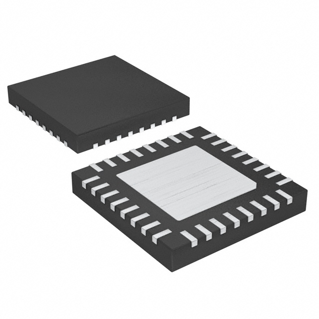


 工商网监
湘ICP备2023018690号
工商网监
湘ICP备2023018690号
