NCP3136
Integrated Synchronous
Buck Converter
6A
3136
ALYWG
G
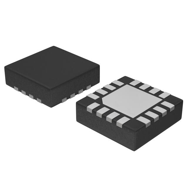
QFN16
CASE 485DA
3136
= Specific Device Code
A
= Assembly Location
L
= Wafer Lot
Y
= Year
W
= Work Week
G
= Pb−Free Package
(Note: Microdot may be in either location)
PINOUT DIAGRAM
EN
1
NC
2
VIN
High Efficiency in Both CCM and DCM
Operation Frequency: 1.1 MHz
Support MLCC Output Capacitor
Small Footprint, 3 mm x 3 mm, 16−pin QFN Package
2.9 V to 5.5 V Wide Conversion Voltage Range
Output Voltage Range from 0.6 V to 0.84 X VIN
Automatic Power−Saving Mode
Voltage Mode Control
Support Pre−bias Start−up Functionality
Output Discharge Operation
Over−Temperature Protection
Built−in Over−Voltage, Under−Voltage and Over−Current Protection
Power Good Indicator
This Device is Pb−Free and is RoHS Compliant
1
VIN
•
•
•
•
•
•
•
•
•
•
•
•
•
•
MARKING
DIAGRAM
PGND
Features
www.onsemi.com
PGND
NCP3136 is a fully integrated synchronous buck converter for 3.3 V
and 5 V step−down applications. It can provide up to 6.5 A
instantaneous current. NCP3136 supports high efficiency, fast
transient response and provides power good indicator. The control
scheme includes two operation modes: FCCM and automatic
CCM/DCM. In automatic CCM/DCM mode, the controller can
smoothly switch between CCM and DCM, where converter runs at
reduced switching frequency with much higher efficiency. NCP3136
is available in 3 mm x 3 mm QFN16 pin package.
16
15
14
13
12 VDD
11 AGND
NCP3136
PGD
3
10 FB
VBST
4
9
5
6
7
8
SW
SW
PS
• 5 V Step Down Rail
• 3.3 V Step Down Rail
SW
Applications
COMP
ORDERING INFORMATION
Device
NCP3136MNTXG
Package
Shipping†
QFN16
(Pb−Free)
3000 / Tape &
Reel
†For information on tape and reel specifications,
including part orientation and tape sizes, please
refer to our Tape and Reel Packaging Specification
Brochure, BRD8011/D.
© Semiconductor Components Industries, LLC, 2017
August, 2019 − Rev. 3
1
Publication Order Number:
NCP3136/D
�NCP3136
VIN
BST
UVLO
NC
OSC
PS
SS
EN
Ramp
Control Logic
&
PWM Logic
Mode
Selection
DRVH
SWN
COMP
VREF
FB
+
+ E/A
−
Power Good
UVP, OVP, UVLO,
Overtemperature
and Vout discharge
PGD
DRVL
OCP
AGND
Figure 1. Block Diagram
PIN DESCRIPTION
Pin No.
Symbol
Description
1
EN
Logic control to enabling the switcher. Internally pulled up to VDD with a 1.35 MW resistor.
2
NC
Not connected.
3
PGD
Open drain power good output.
4
BST
Gate drive voltage for high side FET. Connect capacitor from this pin to SWN.
5,6,7
SWN
Switch node between high−side MOSFET and low−side MOSFET.
8
PS
9
COMP
10
FB
11
AGND
12
VDD
Power supply input for control circuitry.
13,14
VIN
Power input for power conversion and gate driver supply.
15,16
PGND
Mode configuration pin:
Connecting to ground: Forced CCM
Pulled high or floating (internal pulled high): Forced CCM
Connect with 24.3 kW to GND: Automatic CCM/DCM
Connect with 57.6 kW to GND: Automatic CCM/DCM
Connect with 105 kW to GND: Automatic CCM/DCM
Connect with 174 kW to GND: Automatic CCM/DCM
Output of the error amplifier.
Feedback pin. Connect to resistor divider to set up the desired output voltage.
Analog ground
Power ground
www.onsemi.com
2
PGND
VDD
�NCP3136
L1
Vin =2.9V~5.5V
C5
C6
C4
13
14
VIN
12 VDD
VIN
5
6
7
C7
Vin
SW SW SW
R7
VBST 4
C8
C9
11 AGND
NCP3136
2
EN
NC
PGD 3
1 EN
R5
8 PS
PGD
R3
FB 10
PGND
PGND
15
16
COMP 9
C2
R4
C1
R1
R2
C3
Figure 2. Application Circuit
www.onsemi.com
3
Vout
�NCP3136
ABSOLUTE MAXIMUM RATINGS
Value
Condition
Min
Max
Unit
VIN, PS
−0.3
6.5
V
VBST
−0.3
17
VBST (with respect to SW)
−0.3
6.5
EN, FB
−0.3
VDD + 0.3
DC
−1
6.5
Pulse < 20 ns, E = 5 mJ
−3
10
PGD
−0.3
6.5
COMP
−0.3
VDD + 0.3
PGND
−0.3
0.3
Operation ambient temperature
TA
−40
125
Storage temperature
TS
−55
150
Junction temperature
TJ
−40
150
Parameter
Input Voltage Range
Output Voltage Range
SW
V
°C
Thermal Characteristics
RqJA
45.4
°C/W
Electrostatic Discharge
Human Body Model (HBM)
2000
V
Charged Device Model (CDM)
2000
Lead temperature 1.6 mm (1/16 inch) from case for 10 seconds
300
°C
Stresses exceeding those listed in the Maximum Ratings table may damage the device. If any of these limits are exceeded, device functionality
should not be assumed, damage may occur and reliability may be affected.
RECOMMENDED OPERATION RATINGS
Value
Parameter
Condition
Input Voltage Range
Min
Typ
Max
Unit
V
VIN
2.9
5.5
VBST
−0.1
13.5
VBST (with respect to SW)
−0.1
6.0
EN, PS, FB
−0.1
VDD
VDD
2.9
5.5
SW
−1
6.5
Output Voltage Range
PGD
−0.1
6.0
COMP
−0.1
VDD
PGND
−0.1
0.1
−40
125
Junction temperature range, TJ
V
°C
Functional operation above the stresses listed in the Recommended Operating Ranges is not implied. Extended exposure to stresses beyond
the Recommended Operating Ranges limits may affect device reliability.
www.onsemi.com
4
�NCP3136
ELECTRICAL CHARACTERISTICS
(VDD = VIN = 3.3 V, TA = TJ = −40°C to +125°C. Typical values are at TA = 25°C, PGND = GND unless otherwise noted)
Parameter
SYMBOL
Test Conditions
Min
VIN
Nominal input voltage range
2.9
Typ
Max
Unit
5.5
V
POWER SUPPLY
VIN operation voltage
VIN UVLO threshold
Ramp up; EN = ‘HI’
VIN UVLO hysteresis
2.8
V
110
mV
VOLTAGE MONITOR
Pull−down voltage with 4 mA sink current
Power good low voltage
Power good high leakage current
60
200
mV
−2.0
0
2.0
mA
Power good threshold
Feedback lower voltage limit
80
83
86
%Vref
Power good threshold
Feedback higher voltage limit
114
117
120
%Vref
Power good high delay
tPGDELAY
400
Output over-voltage protection
threshold at FB
Over-voltage blanking time
TOVPDLY
Time from FB higher than 20% of Vref
to OVP fault
Output under−voltage protection
threshold at FB
Under-voltage blanking time
ms
114
117
120
%Vref
1.0
1.5
2.5
ms
80
83
86
%Vref
TUVPDLY
Time from FB lower than
20% of Vref to UVP fault
11
IVIN
EN = ‘HI’, no switching
1.5
IVIN_SD
EN = ‘LO’
ms
SUPPLY CURRENT (TJ = +25°C)
VIN quiescent current
VIN shutdown supply current
3.5
mA
15
mA
606
mV
FEEDBACK VOLTAGE & ERROR AMPLIFIER
Reference voltage at FB
VREF
594
600
Unity gain bandwidth (Note 1)
14
MHz
Open loop gain (Note 1)
80
dB
FB pin leakage current
100
Output sourcing and sinking
current (Note 1)
Ccomp = 20 pF
Slew rate (Note 1)
nA
5
mA
5
V/ms
OVER CURRENT PROTECTION & ZERO CROSSING
When Iout exceeds this threshold
for 4 consecutive cycles,
VIN = 3.3 V, VOUT = 1.5 V with 1 mH
inductor, Fsw = 1.1 MHz, TA = 25°C
Over−current limit on high−side FET
Hiccup time duration
thiccup
Zero crossing comparator internal
offset (Note 1)
7.6
Fsw = 1.1 MHz
PGND−SWN, Automatic CCM/DCM mode
8.2
8.8
14.5
A
ms
−4.5
−3.0
−1.5
mV
1.1
1.18
1.30
V
EN hysteresis
0.18
0.24
V
EN input pull up resistor
1.2
LOGIC PINS:I/O VOLTAGE AND CURRENT
EN high threshold voltage
MW
Product parametric performance is indicated in the Electrical Characteristics for the listed test conditions, unless otherwise noted. Product
performance may not be indicated by the Electrical Characteristics if operated under different conditions.
1. Guaranteed by design, not production tested.
www.onsemi.com
5
�NCP3136
ELECTRICAL CHARACTERISTICS
(VDD = VIN = 3.3 V, TA = TJ = −40°C to +125°C. Typical values are at TA = 25°C, PGND = GND unless otherwise noted)
Parameter
SYMBOL
Test Conditions
Min
Typ
Max
Unit
LOGIC PINS:I/O VOLTAGE AND CURRENT
PS mode threshold voltage
PS source current
PSTHS
IPS
Level 1 to Level 2
0.05
Level 2 to Level 3
1.3
7 mA pull-up current when enabled
7
V
mA
INTERNAL BST DIODE
VBST = 6.6 V, VIN = 3.3 V, TA = 25°C
Reverse−bias leakage current
1
mA
SOFT STOP
Output discharge on−resistance
EN = 0, VIN = 3.3 V, VOUT = 0.5 V
36
W
Rising from VSS = 0 V to VSS = 0.6 V
1.5
ms
EN = ‘HI’
0.5
ms
TIMERS: SOFT−START
Soft−Start ramp−up time
TSS
Delay after EN asserting
Switching Frequency Control
FCCM mode
Frequency setting = 1.1 MHz
0.99
1.10
1.21
MHz
FCCM mode or
Automatic CCM/DCM mode
100
140
ns
2.9 V< VIN < 6.0 V
VIN/4
PWM
Minimum OFF time
PWM ramp amplitude (Note 1)
Maximum duty cycle, FCCM mode
or Automatic CCM/DCM mode
FSW = 1.1 MHz
84%
89%
130
140
V
THERMAL SHUTDOWN
Thermal shutdown threshold
(Note 1)
Thermal shutdown hysteresis
(Note 1)
40
150
°C
°C
Product parametric performance is indicated in the Electrical Characteristics for the listed test conditions, unless otherwise noted. Product
performance may not be indicated by the Electrical Characteristics if operated under different conditions.
1. Guaranteed by design, not production tested.
www.onsemi.com
6
�NCP3136
TYPICAL CHARACTERISTICS
98
96
96
94
3.3 V
2.5 V
92
1.8 V
90
1.5 V
88
1.2 V
86
VOUT = 1.0 V
82
1.5 V
88
1.2 V
86
0
1
2
3
4
VOUT = 1.0 V
82
80
5
0
1
2
3
4
5
LOAD CURRENT (A)
LOAD CURRENT (A)
Figure 3. Efficiency at Vin = 5.0 V FCCM
Operation Mode
Figure 4. Efficiency at Vin = 5.0 V Auto
CCM/DCM Operation Mode
98
96
96
94
94
2.5 V
92
90
1.8 V
88
1.5 V
86
1.2 V
EFFICIENCY (%)
EFFICIENCY (%)
1.8 V
90
98
84
2.5 V
92
90
1.8 V
88
1.5 V
86
1.2 V
84
82
80
2.5 V
92
84
84
80
EFFICIENCY (%)
EFFICIENCY (%)
94
3.3 V
82
VOUT = 1.0 V
0
1
2
3
4
80
5
VOUT = 1.0 V
0
1
2
3
4
LOAD CURRENT (A)
LOAD CURRENT (A)
Figure 5. Efficiency at Vin = 3.3 V FCCM
Operation Mode
Figure 6. Efficiency at Vin = 3.3 V Auto
CCM/DCM Operation Mode
www.onsemi.com
7
5
�NCP3136
DETAILED DESCRIPTION
Overview
VDD Voltage
NCP3136 is a low input voltage high performance
synchronous buck converter with two integrated
N−MOSFETs. NCP3136’s output voltage range is from
0.6 V to 0.84 x Vin and it has wide input voltage range from
2.9 V to 5.5 V. The features of NCP3136 include supporting
pre−bias start−up to protect sensitive loads, cycle−by−cycle
over−current limiting and short circuit protection, power
good monitor, over voltage and under voltage protection,
built in output discharge and thermal shutdown.
NCP3136 provides two operation modes to fit various
application requirements. The automatic CCM/DCM mode
operation provides reduced power loss and increases the
efficiency at light load. The adaptive power control
architecture enables smooth transition between light load
and heavy load while maintaining fast response to load
transients.
The VDD voltage is supplied from VIN via an intrenal
resistor. Meanwhile, it is also ok to short the VDD pin and
VIN pins externally.
Reference Voltage
The NCP3136 incorporates 600 mV reference voltage
with 1.0% tolerance.
Internal Soft−Start
To limit the start−up inrush current, an internal soft start
circuit is used to ramp up the reference voltage from 0 V to
its final value linearly. The internal soft start time is 2.0 ms
typically.
Soft Stop
Soft−Stop or discharge mode is always on during faults or
disable. In this mode, disable (EN) causes the output to be
discharged through an internal 40 W transistor inside of SW
terminal. The time constant of soft−stop is a function of
output capacitance and the resistance of the discharge
transistor.
Operation Mode
In forced continuous conduction mode (FCCM), the
high−side FET is ON during the on−time and the low−side
FET is ON during the off−time. The switching is
synchronized to an internal clock thus the switching
frequency is fixed.
In Automatic CCM/DCM mode, the high−side FET is ON
during the on−time and low−side FET is ON during the
off−time until the inductor current reaches zero. An internal
zero−crossing comparator detects the zero crossing of the
inductor current from positive to negative. When the
inductor current reaches zero, the comparator sends a signal
to the logic circuitry and turns off the low−side FET.
When the load is increased, the inductor current is always
positive and the zero−crossing comparator does not send any
zero−crossing signal. The converter enters into continuous
conduction mode (CCM) when no zero−crossing is detected
for two consecutive PWM pulses. In CCM mode, the
switching synchronizes to the internal clock and the
switching frequency is fixed.
Automatic Power Saving Mode
In Automatic CCM/DCM mode when the load current
decreases, the converter will enter power saving mode
operation. During power saving mode, the low−side
MOSFET will turn off when the inductor current reaches
zero. So the converter skips switching and operates with
reduced frequency, which minimizes the quiescent current
and maintains high efficiency.
Forced Continuous Conduction Mode
When PS pin is floating or pulled high, NCP3136 is
operating in forced continuous conduction mode in both
light load and heavy load conditions. In this mode, the
switching frequency remains constant over the entire load
range, making it suitable for applications that need tight
regulation of switching frequency at a cost of lower
efficiency at light load.
www.onsemi.com
8
�NCP3136
PROTECTIONS
Under Voltage Lockout (UVLO)
This situation occurs for a number of reasons: the
converter’s output capacitors may have residual charge on
them or the converter’s output may be held up by a low
current standby power supply. NCP3136 supports pre−bias
start up by holding low−side FETs off until soft start ramp
reaches the FB pin voltage.
There is under-voltage lock out protection (UVLO) for
VIN in NCP3136, which has a typical trip threshold voltage
2.8 V and trip hysteresis 130 mV for VIN. If UVLO is
triggered, the device resets and waits for the voltage to rise
up over the threshold voltage and restart the part. Please note
this protection function DOES NOT trigger the fault counter
to latch off the part.
Thermal Shutdown
The NCP3136 protects itself from over heating with an
internal thermal monitoring circuit. When the die
temperature goes beyond a threshold value 135°C, both the
high−side and the low−side FETs turn off until the
temperature falls 40°C below of the threshold value. Then
the converter restarts.
Over Voltage Protection (OVP)
When feedback voltage is above 17% (typical) of nominal
voltage for over 1.7 ms blanking time, an OV fault is set. In
this case, the converter de−asserts the PGD signal and
performs the over−voltage protection function. The top gate
drive is turned off and the bottom gate drive is turned on to
discharge the output. The bottom gate drive will be turned
off until VFB drops below the UVP threshold. The device
enters a high−impedance state. This protection is latched.
Application Note
For higher output voltage application cases (Vout =
3.3 V), choose the inductor value not to be lower than 1 mH
to avoid over-current protection being triggered by inductor
current ripple; For Vin = 5 V and Vout = 3.3 V case, add a
voltage divider between Vin and EN to ensure that the part
can start up without triggering UVP. Use Figure 7 as design
reference for schematics. For other lower output voltage
cases, it is not necessary to add this divider.
Under Voltage Protection (UVP)
Output under−voltage protection works in conjunction
with the current protection described in the Over−current
Protection sections. An UVP circuit monitors the feedback
voltage to detect under−voltage event. The under−voltage
limit is 17% (typical) below of nominal voltage at FB pin.
If the feedback voltage is below this threshold over 11 ms, an
UV fault is set and both the high−side and the low−side FETs
turn off. After a hiccup delay, the part tries to restart. This
protection behavior is hiccup.
VIN = 5 V
10 kW
EN
Power Good Monitor (PGD)
NCP3136 provides window comparator to monitor the
output voltage at FB pin. When the output voltage is within
±17% of regulation voltage, the power good pin outputs a
high signal. Otherwise, PGD stays low. The PGD pin is open
drain 5 mA pull down output. During startup, PGD stays low
until the feedback voltage is within the specified range for
about 0.4 ms. If feedback voltage falls outside the tolerance
band, the PG pin goes low after 10 ms delay.
The PGD pin de−asserts as soon as the EN pin is pulled
low or an under−voltage event on VDD is detected.
3.6 kW
PGND
Figure 7. Voltage divider between VIN and EN for
start−up in VIN = 5 V and VOUT = 3.3 V case
Layout Guidelines
When laying out a power PCB for the NCP3136 there are
several key points to consider.
Use four vias to connect the thermal pad to power ground.
Separate the power ground and analog ground planes;
connect them together at a single point.
Increase the thickness of PCB copper, it can help to lower
the die temperature and improve the overall efficiency but
meanwhile increase the cost of the board fabrication.
Use wide traces for the nodes conducting high current
such as VIN, VOUT, PGND and SW.
Place feedback and compensation network components
close to the IC.
Keep FB, COMP away from noisy signals such as SW,
BST.
Place VIN and VDD decoupling capacitors as close to the
IC as possible.
Over Current Protection (OCP)
NCP3136 provides high−side MOSFET current limiting.
When the current through the high−side FET exceeds 7.5 A,
the high−side FET turns off and the low−side FET turns on
until next PWM cycle. An over−current counter is triggered
and starts to increment each occurrence of an over−current
event. Both the high−side and the low−side FETs turn off
when the OC counter reaches four. The OC counter resets if
the detected current is less than 7.5 A after an OC event.
Pre−Bias Startup
In some applications the controller will be required to start
switching when its output capacitors are charged anywhere
from slightly above 0 V to just below the regulation voltage.
www.onsemi.com
9
�MECHANICAL CASE OUTLINE
PACKAGE DIMENSIONS
QFN16 3x3, 0.5P
CASE 485DA
ISSUE A
1
SCALE 2:1
ÇÇÇÇ
ÇÇÇÇ
ÇÇÇÇ
ÇÇÇÇ
D
PIN ONE
REFERENCE
2X
B
A
DATE 22 SEP 2015
NOTES:
1. DIMENSIONING AND TOLERANCING PER
ASME Y14.5M, 1994.
2. CONTROLLING DIMENSION: MILLIMETERS.
3. DIMENSION b APPLIES TO PLATED
TERMINAL AND IS MEASURED BETWEEN
0.15 AND 0.30 MM FROM THE TERMINAL TIP.
4. COPLANARITY APPLIES TO THE EXPOSED
PAD AS WELL AS THE TERMINALS.
L
L
L1
DETAIL A
E
ALTERNATE
CONSTRUCTIONS
0.10 C
ÉÉÉ
ÇÇÇ
A3
2X
0.10 C
EXPOSED Cu
TOP VIEW
A
DETAIL B
0.05 C
ÉÉÉ
ÉÉÉ
ÇÇÇ
MOLD CMPD
A3
A1
DETAIL B
A3
ALTERNATE
CONSTRUCTIONS
0.05 C
NOTE 4
SIDE VIEW
A1
C
SEATING
PLANE
D2
16X
5
L
8X
0.10 C A B
16X
1
b
0.10 C A B
0.05 C
K
XXXXX
XXXXX
ALYWG
G
L2
9
E2
NOTE 3
16
e
e/2
BOTTOM VIEW
XXXXX
A
L
Y
W
G
= Specific Device Code
= Assembly Location
= Wafer Lot
= Year
= Work Week
= Pb−Free Package
(Note: Microdot may be in either location)
*This information is generic. Please refer to
device data sheet for actual part marking.
Pb−Free indicator, “G” or microdot “ G”,
may or may not be present.
RECOMMENDED
SOLDERING FOOTPRINT*
3.30
PACKAGE
OUTLINE
MILLIMETERS
MIN
MAX
0.80
1.00
0.00
0.05
0.20 REF
0.20
0.30
3.00 BSC
1.55
1.75
3.00 BSC
1.55
1.75
0.50 BSC
0.275 REF
0.30
0.50
0.00
0.15
0.09 REF
GENERIC
MARKING DIAGRAM*
0.10 C A B
DETAIL A
DIM
A
A1
A3
b
D
D2
E
E2
e
K
L
L1
L2
16X
0.61
1.78
1
1.78 3.30
16X
0.30
0.50
PITCH
DIMENSIONS: MILLIMETERS
*For additional information on our Pb−Free strategy and soldering
details, please download the ON Semiconductor Soldering and
Mounting Techniques Reference Manual, SOLDERRM/D.
DOCUMENT NUMBER:
DESCRIPTION:
98AON87551E
QFN16, 3X3, 0.5P
Electronic versions are uncontrolled except when accessed directly from the Document Repository.
Printed versions are uncontrolled except when stamped “CONTROLLED COPY” in red.
PAGE 1 OF 1
ON Semiconductor and
are trademarks of Semiconductor Components Industries, LLC dba ON Semiconductor or its subsidiaries in the United States and/or other countries.
ON Semiconductor reserves the right to make changes without further notice to any products herein. ON Semiconductor makes no warranty, representation or guarantee regarding
the suitability of its products for any particular purpose, nor does ON Semiconductor assume any liability arising out of the application or use of any product or circuit, and specifically
disclaims any and all liability, including without limitation special, consequential or incidental damages. ON Semiconductor does not convey any license under its patent rights nor the
rights of others.
© Semiconductor Components Industries, LLC, 2019
www.onsemi.com
�onsemi,
, and other names, marks, and brands are registered and/or common law trademarks of Semiconductor Components Industries, LLC dba “onsemi” or its affiliates
and/or subsidiaries in the United States and/or other countries. onsemi owns the rights to a number of patents, trademarks, copyrights, trade secrets, and other intellectual property.
A listing of onsemi’s product/patent coverage may be accessed at www.onsemi.com/site/pdf/Patent−Marking.pdf. onsemi reserves the right to make changes at any time to any
products or information herein, without notice. The information herein is provided “as−is” and onsemi makes no warranty, representation or guarantee regarding the accuracy of the
information, product features, availability, functionality, or suitability of its products for any particular purpose, nor does onsemi assume any liability arising out of the application or use
of any product or circuit, and specifically disclaims any and all liability, including without limitation special, consequential or incidental damages. Buyer is responsible for its products
and applications using onsemi products, including compliance with all laws, regulations and safety requirements or standards, regardless of any support or applications information
provided by onsemi. “Typical” parameters which may be provided in onsemi data sheets and/or specifications can and do vary in different applications and actual performance may
vary over time. All operating parameters, including “Typicals” must be validated for each customer application by customer’s technical experts. onsemi does not convey any license
under any of its intellectual property rights nor the rights of others. onsemi products are not designed, intended, or authorized for use as a critical component in life support systems
or any FDA Class 3 medical devices or medical devices with a same or similar classification in a foreign jurisdiction or any devices intended for implantation in the human body. Should
Buyer purchase or use onsemi products for any such unintended or unauthorized application, Buyer shall indemnify and hold onsemi and its officers, employees, subsidiaries, affiliates,
and distributors harmless against all claims, costs, damages, and expenses, and reasonable attorney fees arising out of, directly or indirectly, any claim of personal injury or death
associated with such unintended or unauthorized use, even if such claim alleges that onsemi was negligent regarding the design or manufacture of the part. onsemi is an Equal
Opportunity/Affirmative Action Employer. This literature is subject to all applicable copyright laws and is not for resale in any manner.
PUBLICATION ORDERING INFORMATION
LITERATURE FULFILLMENT:
Email Requests to: orderlit@onsemi.com
onsemi Website: www.onsemi.com
◊
TECHNICAL SUPPORT
North American Technical Support:
Voice Mail: 1 800−282−9855 Toll Free USA/Canada
Phone: 011 421 33 790 2910
Europe, Middle East and Africa Technical Support:
Phone: 00421 33 790 2910
For additional information, please contact your local Sales Representative
�


 工商网监
湘ICP备2023018690号
工商网监
湘ICP备2023018690号
