NCP5500, NCV5500,
NCP5501, NCV5501
LDO Voltage Regulator
500 mA
These linear low drop voltage regulators provide up to 500 mA over
a user−adjustable output range of 1.25 V to 5.0 V, or at a fixed output
voltage of 1.5 V, 3.3 V or 5.0 V, with typical output voltage accuracy
better than 3%. An internal PNP pass transistor permits low dropout
voltage and operation at full load current at the minimum input
voltage. NCV versions are qualified for demanding automotive
applications that require extended temperature operation and site and
change control. NCP5500 and NCV5500 versions include an
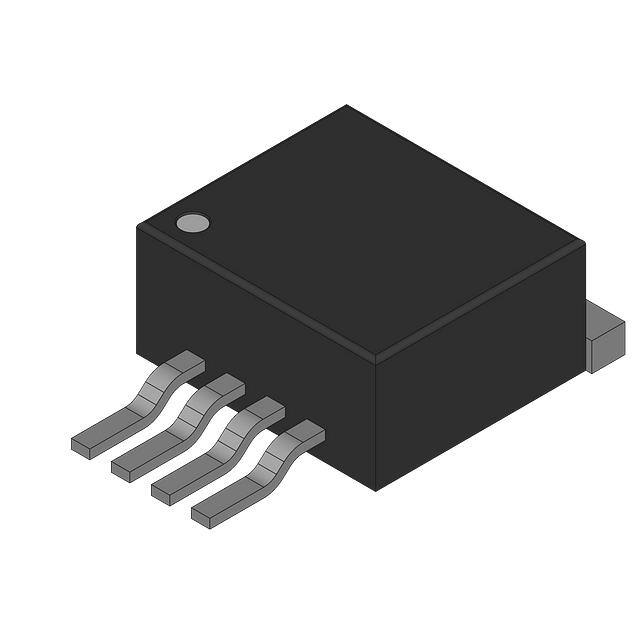
Enable/Shutdown function and are available in a DPAK 5 and SOIC 8
packages. NCP5501 and NCV5501 versions are available in DPAK 3
for applications that do not require logical on/off control.
This regulator family is ideal for applications that require a broad
input voltage range, and low dropout performance up to 500 mA load
using low cost ceramic capacitors. Integral protection features include
short circuit current and thermal shutdown.
Features
•
•
•
•
•
•
•
•
•
•
•
Output Current up to 500 mA
2.9% Output Voltage Accuracy
Low Dropout Voltage (230 mV at 500 mA)
Enable Control Pin (NCP5500 / NCV5500)
Reverse Bias Protection
Short Circuit Protection
Thermal Shutdown
Wide Operating Temperature Range
NCV5500 / NCV5501; −40°C to +125°C Ambient Temperature
NCP5500 / NCP5501; −40°C to +85°C Ambient Temperature
NCV Prefix for Automotive and Other Applications Requiring
Unique Site and Control Change Requirements; AEC−Q100
Qualified and PPAP Capable
Stable with Low Cost Ceramic Capacitors
These are Pb−Free Devices
MARKING DIAGRAMS
DPAK 5
CENTER LEAD CROP
CASE 175AA
1
5
Pin 1. EN
2. Vin
TAB,3. GND
4. Vout
5. NC/ADJ
4
1 2
3
Pin 1. Vin
TAB,2. GND
3. Vout
Automotive
Industrial and Consumer
Post SMPS Regulation
Point of Use Regulation
x5500yG
ALYWW
1
DPAK 3
SINGLE GAUGE
CASE 369C
5
x5501yG
ALYWW
1
3
x
= P (NCP), V (NCV)
5500/1 = Device Code
y
= Output Voltage
= L = 1.5 V
= T = 3.3 V
= U = 5.0 V
= W = Adjustable
A
= Assembly Location
L
= Wafer Lot
Y
= Year
WW
= Work Week
G
= Pb−Free Package
8
SOIC−8
CASE 751
8
1
Pin 1. Vin
2. GND
3. GND
4. Vout
5. NC/ADJ
6. GND
7. GND
8. EN
Typical Applications
•
•
•
•
http://onsemi.com
1
5500x
ALYW
G
x = Output Voltage, NCP/NCV
A = Adjustable, NCV
B = Adjustable, NCP
A = Assembly Location
L = Wafer Lot
Y = Year
W = Work Week
G = Pb−Free Package
ORDERING INFORMATION
See detailed ordering and shipping information in the package
dimensions section on page 10 of this data sheet.
© Semiconductor Components Industries, LLC, 2013
September, 2019 − Rev. 12
1
Publication Order Number:
NCP5500/D
�NCP5500, NCV5500, NCP5501, NCV5501
NCP5500
NCV5500
NCP5501
NCV5501
Vout
Vin
Input
Output
Cin
10 mF
Enable
Cout
4.7 mF
EN*
OFF ON
GND
R1 *
NC/ADJ*
RL
R2 *
GND
*Applicable to NCP5500/NCV5500 only.
Figure 1. Typical Application Circuit
PIN FUNCTION DESCRIPTIONS
DPAK 3
DPAK 5
SOIC−8
Pin No.
Pin No.
Pin No.
Pin
Name
−
1
8
EN
Enable. This pin allows for on/off control of the regulator. High level turns on the
output. To disable the device, connect to ground. If this function is not in use, connect to Vin.
Positive power supply input voltage.
Description
1
2
1
Vin
2, Tab
3, Tab
2, 3, 6, 7
GND
Ground. This pin is internally connected to the Tab heat sink.
3
4
4
Vout
Regulated output voltage.
−
5
5
NC/ADJ
No connection (Fixed output versions).
Voltage−adjust input (Adjustable output version). Use an external voltage divider
to set the output voltage over a range of 1.25 V to 5.0 V.
Vin
Vout
Bandgap
Reference
Error
Amplifier
Current Limit and
Saturation Sense
−
+
Thermal
Shutdown
Connection for Fixed Output
EN*
Enable
Block*
GND
Connection for Adjustable Output
NC / ADJ*
*Applicable to NCP5500/NCV5500 only.
Figure 2. Block Diagram
http://onsemi.com
2
�NCP5500, NCV5500, NCP5501, NCV5501
ABSOLUTE MAXIMUM RATINGS
Symbol
Min
Max
Unit
Input Voltage (Note 1)
Rating
Vin
−0.3 (Note 2)
+18
V
Output, Enable Voltage
Vout, EN
−0.3
+16 or
Vin + 0.3
(Notes 2 and 5)
V
Maximum Junction Temperature
Storage Temperature
Moisture Sensitivity Level
All Packages
TJ
−
150
°C
TStg
−55
+150
°C
MSL
Lead Temperature Soldering
Reflow (SMD Styles Only), Pb−Free Versions (Note 3)
1
Tsld
−
265 Peak
°C
ESD Capability, Human Body Model (Note 4)
ESDHBM
4000
−
V
ESD Capability, Machine Model (Note 4)
ESDMM
200
−
V
ESD Capability, Charged Device Model (Note 4)
ESDCDM
1000
−
V
Stresses exceeding Maximum Ratings may damage the device. Maximum Ratings are stress ratings only. Functional operation above the
Recommended Operating Conditions is not implied. Extended exposure to stresses above the Recommended Operating Conditions may affect
device reliability.
*Latchup Current Maximum Rating: ≤ 100 mA per JEDEC standard: JESD78.
1. Refer to Electrical Characteristics and Application Information for Safe Operating Area.
2. Reverse bias protection feature valid only if Vout − Vin v 7 V.
3. Pb−Free, 60 sec –150 sec above 217°C, 40 sec max at peak temperature
4. This device series incorporates ESD protection and is tested by the following methods:
ESD Human Body Model tested per AEC−Q100−002 (EIA/JESD22−A114)
ESD Machine Model tested per AEC−Q100−003 (EIA/JESD22−A115)
ESD Charged Device Model tested per EIA/JES D22/C101, Field Induced Charge Model
5. Maximum = +16 V or (Vin + 0.3 V), whichever is lower.
THERMAL CHARACTERISTICS
Rating
Symbol
Max
Unit
PD
Internally Limited
W
Thermal Characteristics, DPAK 3 and DPAK 5 (Note 1)
Thermal Resistance, Junction−to−Air (Note 6)
Thermal Resistance, Junction−to−Case
RqJA
RqJC
60
5.2
Thermal Characteristics, SOIC−8 (Note 1)
Thermal Resistance, Junction−to−Air (Note 6)
Thermal Reference, Junction−to−Lead
RqJA
RYJL
80
22
Package Dissipation
Min
°C/W
°C/W
6. As measured using a copper heat spreading area of 650 mm2, 1 oz copper thickness.
OPERATING RANGES
Rating
Symbol
Min
Max
Unit
Operating Input Voltage (Note 1)
Vin
Vout + VDO, 2.5 V
(Note 7)
16
V
Adjustable Output Voltage Range (Adjustable Version Only)
Vout
1.25
5.0
V
−40
−40
85
125
Operating Ambient Temperature Range
NCP5500, NCP5501
NCV5500, NCV5501
TA
7. Minimum Vin = 2.5 V or (Vout + VDO), whichever is higher.
http://onsemi.com
3
°C
�NCP5500, NCV5500, NCP5501, NCV5501
ELECTRICAL CHARACTERISTICS Vin = 2.5 V or Vout + 1.0 V (whichever is higher), Cin = 10 mF, Cout = 4.7 mF, for typical values TA
= 25°C, for min/max values TA = −40°C to 85°C (NCP Version), TA = −40°C to 125°C (NCV Version) unless otherwise noted (Note 13).
Characteristic
Symbol
Test Conditions
Min
Typ
Max
Unit
OUTPUT
Output Voltage (Note 14)
5 V Regulator
3.3 V Regulator
1.5 V Regulator
ADJ Regulator
Output Voltage (Note 8)
5 V Regulator
3.3 V Regulator
1.5 V Regulator
ADJ Regulator
VNOM±2.9%
Vout
V
V
V
TA = 25°C, Iout = 50 mA
(−4.9%)
4.755
3.138
1.427
1.189
VNOM
5.0
3.3
1.5
1.25
(+4.9%)
5.245
3.462
1.574
1.311
V
V
V
Vout
1.0 mA < Iout < 500 mA
Line Regulation
REGLINE
Iout = 50 mA
2.5 V or (Vout + 1.0 V) < Vin < 16 V
−1.0
0.1
1.0
%
Load Regulation
REGLOAD
1.0 mA < Iout < 500 mA
−1.0
0.35
1.0
%
Iout = 1.0 mA, DVout = −2%
Iout = 500 mA, DVout = −2%
Iout = 1.0 mA, DVout = −2%
Iout = 500 mA, DVout = −2%
Iout = 1.0 mA, DVout = −2%
Iout = 500 mA, DVout = −2%
Iout = 1.0 mA, DVout = −2%
Iout = 500 mA, DVout = −2%
−
−
−
−
−
−
−
−
5
230
5
230
−
−
5
230
90
700
90
700
1073
1073
90
700
Dropout Voltage (Note 9)
5.0 V Version
VDO
3.3 V Version
1.5 V Version (Note 10)
Adjustable Version (Note 11)
Ground Current
mV
IGND
Iout = 100 mA
Iout = 500 mA
300
10
500
20
mA
mA
ISD
Adjustable and 1.5 V versions
All other versions
30
40
50
50
mA
Iout(LIM)
Vout = 90% of Vout(nom)
500
700
900
mA
Ripple Rejection Ratio (Notes 9 & 14)
RR
120 Hz
Iout = 100 mA, 1 kHz
10 kHz
−
−
−
75
75
70
−
−
−
dB
Output Noise Voltage (Notes 12 & 14)
Vn
f = 10 Hz to 100 kHz, Vin = 2.5 V
Vout = 1.25 V, Iout = 1.0 mA
18
f = 10 Hz to 100 kHz, Vin = 2.5 V
Vout = 1.25 V, Iout = 100 mA
35
Disable Current in Shutdown
(NCP5500, NCV5500)
Current Limit
mVrms
ENABLE (NCP5500, NCV5500 Only)
Enable Voltage
Enable Pin Bias Current
VENoff
VENon
OFF (shutdown) State
ON (enabled) State
IEN
VEN = Vin, Iout = 1.0 mA
IADJ
VEN = Vin, VADJ = 1.25 V, Vout = 1.25 V
TSD
Iout = 100 mA
0.4
V
−
1.0
mA
−
60
nA
−
210
°C
2.0
ADJUST
Adjust Pin Current (Note 14)
THERMAL SHUTDOWN
Thermal Shutdown Temperature (Note 14)
150
8. Deviation from nominal. For adjustable versions, Pin ADJ connected to Vout.
9. See Typical Characteristics section for additional information.
10. VDO is constrained by the minimum input voltage of 2.5 V.
11. Vout is set by external resistor divider to 5 V.
12. Vn for other fixed voltage versions, as well as adjustable versions set to other output voltages, can be calculated from the following formula:
Vn = Vn(x) * Vout / 1.25, where Vn(x) is the typical value from the table above.
13. Performance guaranteed over specified operating conditions by design, guard banded test limits, and/or characterization, production tested
at TJ = TA = 25°C. Low duty cycle pulse techniques are used during testing to maintain the junction temperature as close to ambient as
possible.
14. Values are based on design and/or characterization.
http://onsemi.com
4
�NCP5500, NCV5500, NCP5501, NCV5501
TYPICAL CHARACTERISTICS
3.45
5.25
3.42
Vin = 13.2 V
RL = 1 kW
5.15
Vout, OUTPUT VOLTAGE (V)
Vout, OUTPUT VOLTAGE (V)
5.20
5.10
5.05
5.00
4.95
4.90
4.85
4.80
4.75
−40
Vout(nom) = 5 V
0
40
80
120
3.30
3.27
3.24
3.21
3.18
Vout(nom) = 3.3 V
0
40
80
120
TA, AMBIENT TEMPERATURE (°C)
Figure 3. Output Voltage vs. Ambient
Temperature
Figure 4. Output Voltage vs. Ambient
Temperature
1.30
1.29
Vin = 13.2 V
RL = 1 kW
1.56
Vout, OUTPUT VOLTAGE (V)
Vout, OUTPUT VOLTAGE (V)
3.33
TA, AMBIENT TEMPERATURE (°C)
1.54
1.52
1.50
1.48
1.46
1.44
1.42
−40
0
40
Vin = 13.2 V
RL = 1 kW
1.28
1.27
1.26
1.25
1.24
1.23
1.22
Vout(nom) = 1.5 V
1.21
80
1.20
−40
120
Vout(nom) = 1.25 V (ADJ)
0
40
80
120
TA, AMBIENT TEMPERATURE (°C)
TA, AMBIENT TEMPERATURE (°C)
Figure 5. Output Voltage vs. Ambient
Temperature
Figure 6. Output Voltage vs. Ambient
Temperature
500
400
TA = 125°C
300
TA = 25°C
TA = −40°C
200
100
Vout(nom) = 5 V
0
100
200
300
400
500
VDO DROPOUT VOLTAGE (mV)
500
VDO, DROPOUT VOLTAGE (mV)
3.36
3.15
−40
1.58
0
Vin = 13.2 V
RL = 1 kW
3.39
450
400
350
TA = 25°C
250
200
150
TA = −40°C
100
50
0
600
TA = 125°C
300
Vout(nom) = 3.3 V
0
100
200
300
400
500
600
Iout, OUTPUT CURRENT (mA)
Iout, OUTPUT CURRENT (mA)
Figure 7. Dropout Voltage vs. Output Current
Figure 8. Dropout Voltage vs. Output Current
http://onsemi.com
5
�NCP5500, NCV5500, NCP5501, NCV5501
TYPICAL CHARACTERISTICS
18
14
12
TA = 25°C
10
TA = 125°C
8
6
4
2
0
Vout(nom) = 5 V
0
100
200
300
400
500
600
TA = 25°C
10
8
TA = 125°C
6
4
2
Vout(nom) = 1.25 V (ADJ)
0
0
700
100
200
300
400
500
600
700
Figure 9. Ground Current vs. Output Current
Figure 10. Ground Current vs. Output Current
Vout(nom) = 5 V
RL = 1 kW
3
2
1
0
1
2
3
4
5
6
Vout(nom) = 3.3 V
RL = 1 kW
5
4
3
2
1
0
7
0
1
2
3
4
5
6
7
Vin, INPUT VOLTAGE (V)
Vin, INPUT VOLTAGE (V)
Figure 11. Ground Current vs. Input Voltage
Figure 12. Ground Current vs. Input Voltage
6
RL = 1 kW
5
Vout(nom) = 1.5 V
4
3
2
1
0
1
2
3
4
5
6
IGND, GROUND CURRENT (mA)
6
IGND, GROUND CURRENT (mA)
12
Iout, OUTPUT CURRENT (mA)
4
0
TA = −40°C
14
6
5
0
16
Iout, OUTPUT CURRENT (mA)
6
IGND, GROUND CURRENT (mA)
IGND, GROUND CURRENT (mA)
TA = −40°C
16
IGND, GROUND CURRENT (mA)
IGND, GROUND CURRENT (mA)
18
RL = 1 kW
5
Vout(nom) = 1.25 V (ADJ)
4
3
2
1
0
7
Vin, INPUT VOLTAGE (V)
0
3
4
5
Vin, INPUT VOLTAGE (V)
Figure 13. Ground Current vs. Input Voltage
Figure 14. Ground Current vs. Input Voltage
http://onsemi.com
6
1
2
6
7
�NCP5500, NCV5500, NCP5501, NCV5501
TYPICAL CHARACTERISTICS
90
1 mA
80
70
60
500 mA
50
40
100 mA
30
Vin = 6 V,
DVin = 0.5 Vpp
20
10
0
RR, RIPPLE REJECTION (dB)
RR, RIPPLE REJECTION (dB)
90
Vout(nom) = 1.5 V
0.01
0.1
1
10
100
500 mA
50
40
30
Vin = 6 V,
DVin = 0.5 Vpp
20
10
Vout(nom) = 1.25 V (ADJ)
0.01
0.1
1
10
Figure 15. Ripple Rejection vs. Frequency
Figure 16. Ripple Rejection vs. Frequency
100
12
11
10
9
7
8
6
Unstable Region
ESR (W)
ESR (W)
60
f, FREQUENCY (kHz)
8
5
4
3
50
100 150 200
Unstable Region
6
5
Stable Region
3
2
Cout = 1 mF to 10 mF
Vout(nom) = 5 V
0
7
4
Stable Region
2
250 300 350
Cout = 1 mF to 10 mF
Vout(nom) = 3.3 V
1
0
400 450 500
0
50
100 150 200 250 300 350 400 450 500
Iout, OUTPUT CURRENT (mA)
Iout, OUTPUT CURRENT (mA)
Figure 17. Output Capacitor ESR Stability vs.
Output Current
Figure 18. Output Capacitor ESR Stability vs.
Output Current
10
10
9
9
8
8
7
7
Unstable Region
6
ESR (W)
ESR (W)
100 mA
f, FREQUENCY (kHz)
9
5
4
Unstable Region
6
5
4
3
3
Stable Region
2
1
0
1 mA
70
0
10
1
0
80
0
50
100 150 200
250 300 350
Stable Region
2
Cout = 1 mF to 10 mF
Vout(nom) = 1.5 V
1
0
400 450 500
0
Iout, OUTPUT CURRENT (mA)
50
Cout = 1 mF to 10 mF
Vout(nom) = 1.25 V (ADJ)
100 150 200 250 300 350 400 450 500
Iout, OUTPUT CURRENT (mA)
Figure 19. Output Capacitor ESR Stability vs.
Output Current
Figure 20. Output Capacitor ESR Stability vs.
Output Current
NOTE: Typical characteristics were measured with the same conditions as electrical characteristics, unless otherwise noted.
http://onsemi.com
7
�NCP5500, NCV5500, NCP5501, NCV5501
NCP5500
Iin
Input
Cin
10 mF
NCV5500
Vout
Vin
Cin2
100 nF
Iout
Cout
Enable
EN
IEN
Output
GND
ADJ
IADJ
RL
IGND
IQ
NCP5501
Iin
Input
Cin
10 mF
NCV5501
Vout
Vin
Cin2
100 nF
Iout
Output
Cout
RL
GND
IGND
IQ
Figure 21. Measuring Circuits
Circuit Description
linear regulator: startup delay, load transient response and
loop stability. The capacitor value and type should be based
on cost, availability, size and temperature constraints. Refer
to Typical Operating Characteristics for stability regions.
The NCP5500/NCP5501/NCV5500/NCV5501 are
integrated linear regulators with a DC load current
capability of 500 mA. The output voltage is regulated by a
PNP pass transistor controlled by an error amplifier and
band gap reference. The choice of a PNP pass element
provides the lowest possible dropout voltage, particularly at
reduced load currents. Pass transistor base drive current is
controlled to prevent oversaturation. The regulator is
internally protected by both current limit and thermal
shutdown. Thermal shutdown occurs when the junction
temperature exceeds 150°C. The NCV5500 includes an
enable/shutdown pin to turn off the regulator to a low current
drain standby state.
Enable Input (NCP5500, NCV5500)
The enable pin is used to turn the regulator on or off. By
holding the pin at a voltage less than 0.4 V, the output of the
regulator will be turned off to a minimal current drain state.
When the voltage at the Enable pin is greater than 2.0 V, the
output of the regulator will be enabled and rise to the
regulated output voltage. The Enable pin may be connected
directly to the input pin to provide a constant enable to the
regulator.
Active Load Protection in Shutdown (NCP5500,
Regulator
NCV5500)
The error amplifier compares the reference voltage to a
sample of the output voltage (Vout) and drives the base of a
PNP series pass transistor via a buffer. The reference is a
bandgap design for enhanced temperature stability.
Saturation control of the PNP pass transistor is a function of
the load current and input voltage. Oversaturation of the
output power device is prevented, and quiescent current in
the ground pin is minimized.
When a linear regulator is disabled (shutdown), the output
(load) voltage should be zero. However, stray PC board
leakage paths, output capacitor dielectric absorption, and
inductively coupled power sources can cause an undesirable
regulator output voltage if load current is low or zero. The
NCV5500 features a load protection network that is active
only during Shutdown mode. This network switches in a
shunt current path (~500 mA) from Vout to Ground. This
feature also provides a controlled (“soft”) discharge path for
the output capacitor after a transition from Enable to
Shutdown.
Regulator Stability Considerations
The input capacitor is necessary to stabilize the input
impedance to reduce transient line influences. The output
capacitor helps determine three main characteristics of a
http://onsemi.com
8
�NCP5500, NCV5500, NCP5501, NCV5501
Ripple Rejection: The ratio of the peak−to−peak input ripple
voltage to the peak−to−peak output ripple voltage.
Current Limit: Peak current that can be delivered to the
output.
Calculating Resistors for the ADJ Versions
The adjustable version uses feedback resistors to adjust
the output to the desired output voltage. With Vout connected
to ADJ, the adjustable version will regulate at 1.25 V
�4.9% (1250 � 61.25 mV).
Output voltage formula with an external resistor divider:
V out +
ǒ
ƪ
1.25 V * 60E−9 @
(R 1 @ R 2)
(R 1 ) R 2)
ƫǓ ǒ
@
(R1 ) R2)
R2
Calculating Power Dissipation
The maximum power dissipation for a single output
regulator (Figure 21) is:
Ǔ
(eq. 1)
P D(max) + ƪV in(max) * V out(min)ƫI out(max) ) V in(max)I GND
Where
R1 = value of the divider resistor connected between Vout
and ADJ,
R2 = value of the divider resistor connected between ADJ
and GND,
The term “1.25 V” has a tolerance of �4.9%; the term
“60E−9” can vary in the range 15E−9 to 60E−9.
For values of R2 less than 15 KW, the term within brackets
( [ ] ) will evaluate to less than 1 mV and can be ignored. This
simplifies the output voltage formula to:
Vout = 1.25 V * ((R1 + R2) / R2)) with a tolerance of �4.9%,
which is the tolerance of the 1.25 V output when delivering
up to 500 mA of output current.
Where
Vin(max) is the maximum input voltage,
Vout(min) is the minimum output voltage,
Iout(max) is the maximum output current for the application,
IGND is the ground current at Iout(max).
Once the value of PD(max) is known, the maximum
permissible value of RqJA can be calculated:
R qJA +
ǒ150°C * T AǓ
PD
(eq. 2)
The value of RqJA can then be compared with those in the
Thermal Characteristics table. Those packages with RqJA
less than the calculated value in Equation 2 will keep the die
temperature below 150°C.
In some cases, none of the packages will be sufficient to
dissipate the heat generated by the IC, and an external heat
sink will be required.
DEFINITION OF TERMS
Dropout Voltage: The input−to−output voltage differential
at which the circuit ceases to regulate against further
reduction input voltage. Measured when the output voltage
has dropped 2% relative to the value measured at nominal
input voltage. Dropout voltage is dependent upon load
current and junction temperature.
Input Voltage: The DC voltage applied to the input
terminals with respect to ground.
Line Regulation: The change in output voltage for a change
in the input voltage. The measurement is made under
conditions of low dissipation or by using pulse techniques
such that the average chip temperature is not significantly
affected.
Load Regulation: The change in output voltage for a change
in load current at constant chip temperature. Pulse loading
techniques are employed such that the average chip
temperature is not significantly affected.
Quiescent and Ground Current: The quiescent current is
the current which flows through the ground when the LDO
operates without a load on its output: internal IC operation,
bias, etc. When the LDO becomes loaded, this term is called
the Ground current. It is actually the difference between the
input current (measured through the LDO input pin) and the
output current.
Heat Sinks
A heat sink effectively increases the surface area of the
package to improve the flow of heat away from the IC and
into the surrounding air.
Each material in the heat flow path between the IC and the
outside environment will have a thermal resistance. Like
series electrical resistances, these resistances are summed to
determine the value of RqJA:
R qJA + R qJC ) R qCS ) R qSA
(eq. 3)
where
RqJC is the junction−to−case thermal resistance,
RqCS is the case−to−heatsink thermal resistance,
RqSA is the heatsink−to−ambient thermal resistance.
RqJC appears in the Thermal Characteristics table. Like
RqJA, it too is a function of package type. RqCS and RqSA are
functions of the package type, heat sink and the interface
between them. These values appear in data sheets of heat
sink manufacturers.
Thermal, mounting, and heat sink considerations are
further discussed in ON Semiconductor Application Note
AN1040/D.
http://onsemi.com
9
�NCP5500, NCV5500, NCP5501, NCV5501
ORDERING INFORMATION
Device
Nominal Output Voltage*
Package
Marking
Package
Shipping†
NCP5500DT15RKG
P5500LG
DPAK 5
(Pb−Free)
2500 / Tape & Reel
NCV5500DT15RKG**
V5500LG
DPAK 5
(Pb−Free)
2500 / Tape & Reel
NCP5501DT15RKG
P5501LG
DPAK 3
(Pb−Free)
2500 / Tape & Reel
V5501LG
DPAK 3
(Pb−Free)
2500 / Tape & Reel
NCP5501DT15G
P5501LG
DPAK 3
(Pb−Free)
75 Units / Rail
NCV5501DT15G**
V5501LG
DPAK 3
(Pb−Free)
75 Units / Rail
NCP5500DT33RKG
P5500TG
DPAK 5
(Pb−Free)
2500 / Tape & Reel
NCV5500DT33RKG**
V5500TG
DPAK 5
(Pb−Free)
2500 / Tape & Reel
NCP5501DT33RKG
P5501TG
DPAK 3
(Pb−Free)
2500 / Tape & Reel
V5501TG
DPAK 3
(Pb−Free)
2500 / Tape & Reel
NCP5501DT33G
P5501TG
DPAK 3
(Pb−Free)
75 Units / Rail
NCV5501DT33G**
V5501TG
DPAK 3
(Pb−Free)
75 Units / Rail
NCP5500DT50RKG
P5500UG
DPAK 5
(Pb−Free)
2500 / Tape & Reel
NCV5500DT50RKG**
V5500UG
DPAK 5
(Pb−Free)
2500 / Tape & Reel
NCP5501DT50RKG
P5501UG
DPAK 3
(Pb−Free)
2500 / Tape & Reel
V5501UG
DPAK 3
(Pb−Free)
2500 / Tape & Reel
NCP5501DT50G
P5501UG
DPAK 3
(Pb−Free)
75 Units / Rail
NCV5501DT50G**
V5501UG
DPAK 3
(Pb−Free)
75 Units / Rail
NCP5500DTADJRKG
P5500WG
DPAK 5
(Pb−Free)
2500 / Tape & Reel
V5500WG
DPAK 5
(Pb−Free)
2500 / Tape & Reel
5500B
SO−8
(Pb−Free)
2500 / Tape & Reel
5500A
SO−8
(Pb−Free)
2500 / Tape & Reel
NCV5501DT15RKG**
NCV5501DT33RKG**
NCV5501DT50RKG**
NCV5500DTADJRKG**
NCP5500DADJR2G
NCV5500DADJR2G**
1.5
3.3
5.0
Adjustable
Adjustable
Adjustable
†For information on tape and reel specifications, including part orientation and tape sizes, please refer to our Tape and Reel Packaging
Specifications Brochure, BRD8011/D.
*Contact ON Semiconductor for other fixed voltages.
**NCV Prefix for Automotive and Other Applications Requiring Unique Site and Control Change Requirements; AEC−Q100 Qualified and PPAP
Capable
http://onsemi.com
10
�MECHANICAL CASE OUTLINE
PACKAGE DIMENSIONS
DPAK−5, CENTER LEAD CROP
CASE 175AA
ISSUE B
DATE 15 MAY 2014
SCALE 1:1
−T−
C
B
V
NOTES:
1. DIMENSIONING AND TOLERANCING
PER ANSI Y14.5M, 1982.
2. CONTROLLING DIMENSION: INCH.
SEATING
PLANE
E
R
R1
Z
A
S
12 3 4 5
U
K
F
J
L
H
D
G
5 PL
0.13 (0.005)
M
T
2.2
0.086
0.34 5.36
0.013 0.217
5.8
0.228
10.6
0.417
0.8
0.031
SCALE 4:1
mm Ǔ
ǒinches
*For additional information on our Pb−Free strategy and soldering
details, please download the ON Semiconductor Soldering and
Mounting Techniques Reference Manual, SOLDERRM/D.
DOCUMENT NUMBER:
DESCRIPTION:
98AON12855D
INCHES
MIN
MAX
0.235 0.245
0.250 0.265
0.086 0.094
0.020 0.028
0.018 0.023
0.024 0.032
0.180 BSC
0.034 0.040
0.018 0.023
0.102 0.114
0.045 BSC
0.170 0.190
0.185 0.210
0.025 0.040
0.020
−−−
0.035 0.050
0.155 0.170
MILLIMETERS
MIN
MAX
5.97
6.22
6.35
6.73
2.19
2.38
0.51
0.71
0.46
0.58
0.61
0.81
4.56 BSC
0.87
1.01
0.46
0.58
2.60
2.89
1.14 BSC
4.32
4.83
4.70
5.33
0.63
1.01
0.51
−−−
0.89
1.27
3.93
4.32
GENERIC
MARKING DIAGRAMS*
RECOMMENDED
SOLDERING FOOTPRINT*
6.4
0.252
DIM
A
B
C
D
E
F
G
H
J
K
L
R
R1
S
U
V
Z
XXXXXXG
ALYWW
AYWW
XXX
XXXXXG
IC
Discrete
XXXXXX
A
L
Y
WW
G
= Device Code
= Assembly Location
= Wafer Lot
= Year
= Work Week
= Pb−Free Package
*This information is generic. Please refer to
device data sheet for actual part marking.
Pb−Free indicator, “G” or microdot “ G”,
may or may not be present.
Electronic versions are uncontrolled except when accessed directly from the Document Repository.
Printed versions are uncontrolled except when stamped “CONTROLLED COPY” in red.
DPAK−5 CENTER LEAD CROP
PAGE 1 OF 1
ON Semiconductor and
are trademarks of Semiconductor Components Industries, LLC dba ON Semiconductor or its subsidiaries in the United States and/or other countries.
ON Semiconductor reserves the right to make changes without further notice to any products herein. ON Semiconductor makes no warranty, representation or guarantee regarding
the suitability of its products for any particular purpose, nor does ON Semiconductor assume any liability arising out of the application or use of any product or circuit, and specifically
disclaims any and all liability, including without limitation special, consequential or incidental damages. ON Semiconductor does not convey any license under its patent rights nor the
rights of others.
© Semiconductor Components Industries, LLC, 2019
www.onsemi.com
�MECHANICAL CASE OUTLINE
PACKAGE DIMENSIONS
DPAK (SINGLE GAUGE)
CASE 369C
ISSUE F
4
1 2
DATE 21 JUL 2015
3
SCALE 1:1
A
E
b3
C
A
B
c2
4
L3
Z
D
1
L4
2
3
NOTE 7
b2
e
c
SIDE VIEW
b
0.005 (0.13)
TOP VIEW
H
DETAIL A
M
BOTTOM VIEW
C
Z
H
L2
GAUGE
PLANE
C
L
L1
DETAIL A
Z
SEATING
PLANE
BOTTOM VIEW
A1
ALTERNATE
CONSTRUCTIONS
ROTATED 905 CW
STYLE 1:
PIN 1. BASE
2. COLLECTOR
3. EMITTER
4. COLLECTOR
STYLE 6:
PIN 1. MT1
2. MT2
3. GATE
4. MT2
STYLE 2:
PIN 1. GATE
2. DRAIN
3. SOURCE
4. DRAIN
STYLE 7:
PIN 1. GATE
2. COLLECTOR
3. EMITTER
4. COLLECTOR
STYLE 3:
PIN 1. ANODE
2. CATHODE
3. ANODE
4. CATHODE
STYLE 8:
PIN 1. N/C
2. CATHODE
3. ANODE
4. CATHODE
STYLE 4:
PIN 1. CATHODE
2. ANODE
3. GATE
4. ANODE
STYLE 9:
STYLE 10:
PIN 1. ANODE
PIN 1. CATHODE
2. CATHODE
2. ANODE
3. RESISTOR ADJUST
3. CATHODE
4. CATHODE
4. ANODE
SOLDERING FOOTPRINT*
6.20
0.244
2.58
0.102
5.80
0.228
INCHES
MIN
MAX
0.086 0.094
0.000 0.005
0.025 0.035
0.028 0.045
0.180 0.215
0.018 0.024
0.018 0.024
0.235 0.245
0.250 0.265
0.090 BSC
0.370 0.410
0.055 0.070
0.114 REF
0.020 BSC
0.035 0.050
−−− 0.040
0.155
−−−
MILLIMETERS
MIN
MAX
2.18
2.38
0.00
0.13
0.63
0.89
0.72
1.14
4.57
5.46
0.46
0.61
0.46
0.61
5.97
6.22
6.35
6.73
2.29 BSC
9.40 10.41
1.40
1.78
2.90 REF
0.51 BSC
0.89
1.27
−−−
1.01
3.93
−−−
GENERIC
MARKING DIAGRAM*
XXXXXXG
ALYWW
AYWW
XXX
XXXXXG
IC
Discrete
= Device Code
= Assembly Location
= Wafer Lot
= Year
= Work Week
= Pb−Free Package
*This information is generic. Please refer to
device data sheet for actual part marking.
Pb−Free indicator, “G” or microdot “G”, may
or may not be present. Some products may
not follow the Generic Marking.
6.17
0.243
SCALE 3:1
DIM
A
A1
b
b2
b3
c
c2
D
E
e
H
L
L1
L2
L3
L4
Z
XXXXXX
A
L
Y
WW
G
3.00
0.118
1.60
0.063
STYLE 5:
PIN 1. GATE
2. ANODE
3. CATHODE
4. ANODE
NOTES:
1. DIMENSIONING AND TOLERANCING PER ASME
Y14.5M, 1994.
2. CONTROLLING DIMENSION: INCHES.
3. THERMAL PAD CONTOUR OPTIONAL WITHIN DIMENSIONS b3, L3 and Z.
4. DIMENSIONS D AND E DO NOT INCLUDE MOLD
FLASH, PROTRUSIONS, OR BURRS. MOLD
FLASH, PROTRUSIONS, OR GATE BURRS SHALL
NOT EXCEED 0.006 INCHES PER SIDE.
5. DIMENSIONS D AND E ARE DETERMINED AT THE
OUTERMOST EXTREMES OF THE PLASTIC BODY.
6. DATUMS A AND B ARE DETERMINED AT DATUM
PLANE H.
7. OPTIONAL MOLD FEATURE.
mm Ǔ
ǒinches
*For additional information on our Pb−Free strategy and soldering
details, please download the ON Semiconductor Soldering and
Mounting Techniques Reference Manual, SOLDERRM/D.
DOCUMENT NUMBER:
DESCRIPTION:
98AON10527D
DPAK (SINGLE GAUGE)
Electronic versions are uncontrolled except when accessed directly from the Document Repository.
Printed versions are uncontrolled except when stamped “CONTROLLED COPY” in red.
PAGE 1 OF 1
onsemi and
are trademarks of Semiconductor Components Industries, LLC dba onsemi or its subsidiaries in the United States and/or other countries. onsemi reserves
the right to make changes without further notice to any products herein. onsemi makes no warranty, representation or guarantee regarding the suitability of its products for any particular
purpose, nor does onsemi assume any liability arising out of the application or use of any product or circuit, and specifically disclaims any and all liability, including without limitation
special, consequential or incidental damages. onsemi does not convey any license under its patent rights nor the rights of others.
© Semiconductor Components Industries, LLC, 2018
www.onsemi.com
�MECHANICAL CASE OUTLINE
PACKAGE DIMENSIONS
SOIC−8 NB
CASE 751−07
ISSUE AK
8
1
SCALE 1:1
−X−
DATE 16 FEB 2011
NOTES:
1. DIMENSIONING AND TOLERANCING PER
ANSI Y14.5M, 1982.
2. CONTROLLING DIMENSION: MILLIMETER.
3. DIMENSION A AND B DO NOT INCLUDE
MOLD PROTRUSION.
4. MAXIMUM MOLD PROTRUSION 0.15 (0.006)
PER SIDE.
5. DIMENSION D DOES NOT INCLUDE DAMBAR
PROTRUSION. ALLOWABLE DAMBAR
PROTRUSION SHALL BE 0.127 (0.005) TOTAL
IN EXCESS OF THE D DIMENSION AT
MAXIMUM MATERIAL CONDITION.
6. 751−01 THRU 751−06 ARE OBSOLETE. NEW
STANDARD IS 751−07.
A
8
5
S
B
0.25 (0.010)
M
Y
M
1
4
−Y−
K
G
C
N
X 45 _
SEATING
PLANE
−Z−
0.10 (0.004)
H
M
D
0.25 (0.010)
M
Z Y
S
X
J
S
8
8
1
1
IC
4.0
0.155
XXXXX
A
L
Y
W
G
IC
(Pb−Free)
= Specific Device Code
= Assembly Location
= Wafer Lot
= Year
= Work Week
= Pb−Free Package
XXXXXX
AYWW
1
1
Discrete
XXXXXX
AYWW
G
Discrete
(Pb−Free)
XXXXXX = Specific Device Code
A
= Assembly Location
Y
= Year
WW
= Work Week
G
= Pb−Free Package
*This information is generic. Please refer to
device data sheet for actual part marking.
Pb−Free indicator, “G” or microdot “G”, may
or may not be present. Some products may
not follow the Generic Marking.
1.270
0.050
SCALE 6:1
INCHES
MIN
MAX
0.189
0.197
0.150
0.157
0.053
0.069
0.013
0.020
0.050 BSC
0.004
0.010
0.007
0.010
0.016
0.050
0 _
8 _
0.010
0.020
0.228
0.244
8
8
XXXXX
ALYWX
G
XXXXX
ALYWX
1.52
0.060
0.6
0.024
MILLIMETERS
MIN
MAX
4.80
5.00
3.80
4.00
1.35
1.75
0.33
0.51
1.27 BSC
0.10
0.25
0.19
0.25
0.40
1.27
0_
8_
0.25
0.50
5.80
6.20
GENERIC
MARKING DIAGRAM*
SOLDERING FOOTPRINT*
7.0
0.275
DIM
A
B
C
D
G
H
J
K
M
N
S
mm Ǔ
ǒinches
*For additional information on our Pb−Free strategy and soldering
details, please download the ON Semiconductor Soldering and
Mounting Techniques Reference Manual, SOLDERRM/D.
STYLES ON PAGE 2
DOCUMENT NUMBER:
DESCRIPTION:
98ASB42564B
SOIC−8 NB
Electronic versions are uncontrolled except when accessed directly from the Document Repository.
Printed versions are uncontrolled except when stamped “CONTROLLED COPY” in red.
PAGE 1 OF 2
onsemi and
are trademarks of Semiconductor Components Industries, LLC dba onsemi or its subsidiaries in the United States and/or other countries. onsemi reserves
the right to make changes without further notice to any products herein. onsemi makes no warranty, representation or guarantee regarding the suitability of its products for any particular
purpose, nor does onsemi assume any liability arising out of the application or use of any product or circuit, and specifically disclaims any and all liability, including without limitation
special, consequential or incidental damages. onsemi does not convey any license under its patent rights nor the rights of others.
© Semiconductor Components Industries, LLC, 2019
www.onsemi.com
�SOIC−8 NB
CASE 751−07
ISSUE AK
DATE 16 FEB 2011
STYLE 1:
PIN 1. EMITTER
2. COLLECTOR
3. COLLECTOR
4. EMITTER
5. EMITTER
6. BASE
7. BASE
8. EMITTER
STYLE 2:
PIN 1. COLLECTOR, DIE, #1
2. COLLECTOR, #1
3. COLLECTOR, #2
4. COLLECTOR, #2
5. BASE, #2
6. EMITTER, #2
7. BASE, #1
8. EMITTER, #1
STYLE 3:
PIN 1. DRAIN, DIE #1
2. DRAIN, #1
3. DRAIN, #2
4. DRAIN, #2
5. GATE, #2
6. SOURCE, #2
7. GATE, #1
8. SOURCE, #1
STYLE 4:
PIN 1. ANODE
2. ANODE
3. ANODE
4. ANODE
5. ANODE
6. ANODE
7. ANODE
8. COMMON CATHODE
STYLE 5:
PIN 1. DRAIN
2. DRAIN
3. DRAIN
4. DRAIN
5. GATE
6. GATE
7. SOURCE
8. SOURCE
STYLE 6:
PIN 1. SOURCE
2. DRAIN
3. DRAIN
4. SOURCE
5. SOURCE
6. GATE
7. GATE
8. SOURCE
STYLE 7:
PIN 1. INPUT
2. EXTERNAL BYPASS
3. THIRD STAGE SOURCE
4. GROUND
5. DRAIN
6. GATE 3
7. SECOND STAGE Vd
8. FIRST STAGE Vd
STYLE 8:
PIN 1. COLLECTOR, DIE #1
2. BASE, #1
3. BASE, #2
4. COLLECTOR, #2
5. COLLECTOR, #2
6. EMITTER, #2
7. EMITTER, #1
8. COLLECTOR, #1
STYLE 9:
PIN 1. EMITTER, COMMON
2. COLLECTOR, DIE #1
3. COLLECTOR, DIE #2
4. EMITTER, COMMON
5. EMITTER, COMMON
6. BASE, DIE #2
7. BASE, DIE #1
8. EMITTER, COMMON
STYLE 10:
PIN 1. GROUND
2. BIAS 1
3. OUTPUT
4. GROUND
5. GROUND
6. BIAS 2
7. INPUT
8. GROUND
STYLE 11:
PIN 1. SOURCE 1
2. GATE 1
3. SOURCE 2
4. GATE 2
5. DRAIN 2
6. DRAIN 2
7. DRAIN 1
8. DRAIN 1
STYLE 12:
PIN 1. SOURCE
2. SOURCE
3. SOURCE
4. GATE
5. DRAIN
6. DRAIN
7. DRAIN
8. DRAIN
STYLE 13:
PIN 1. N.C.
2. SOURCE
3. SOURCE
4. GATE
5. DRAIN
6. DRAIN
7. DRAIN
8. DRAIN
STYLE 14:
PIN 1. N−SOURCE
2. N−GATE
3. P−SOURCE
4. P−GATE
5. P−DRAIN
6. P−DRAIN
7. N−DRAIN
8. N−DRAIN
STYLE 15:
PIN 1. ANODE 1
2. ANODE 1
3. ANODE 1
4. ANODE 1
5. CATHODE, COMMON
6. CATHODE, COMMON
7. CATHODE, COMMON
8. CATHODE, COMMON
STYLE 16:
PIN 1. EMITTER, DIE #1
2. BASE, DIE #1
3. EMITTER, DIE #2
4. BASE, DIE #2
5. COLLECTOR, DIE #2
6. COLLECTOR, DIE #2
7. COLLECTOR, DIE #1
8. COLLECTOR, DIE #1
STYLE 17:
PIN 1. VCC
2. V2OUT
3. V1OUT
4. TXE
5. RXE
6. VEE
7. GND
8. ACC
STYLE 18:
PIN 1. ANODE
2. ANODE
3. SOURCE
4. GATE
5. DRAIN
6. DRAIN
7. CATHODE
8. CATHODE
STYLE 19:
PIN 1. SOURCE 1
2. GATE 1
3. SOURCE 2
4. GATE 2
5. DRAIN 2
6. MIRROR 2
7. DRAIN 1
8. MIRROR 1
STYLE 20:
PIN 1. SOURCE (N)
2. GATE (N)
3. SOURCE (P)
4. GATE (P)
5. DRAIN
6. DRAIN
7. DRAIN
8. DRAIN
STYLE 21:
PIN 1. CATHODE 1
2. CATHODE 2
3. CATHODE 3
4. CATHODE 4
5. CATHODE 5
6. COMMON ANODE
7. COMMON ANODE
8. CATHODE 6
STYLE 22:
PIN 1. I/O LINE 1
2. COMMON CATHODE/VCC
3. COMMON CATHODE/VCC
4. I/O LINE 3
5. COMMON ANODE/GND
6. I/O LINE 4
7. I/O LINE 5
8. COMMON ANODE/GND
STYLE 23:
PIN 1. LINE 1 IN
2. COMMON ANODE/GND
3. COMMON ANODE/GND
4. LINE 2 IN
5. LINE 2 OUT
6. COMMON ANODE/GND
7. COMMON ANODE/GND
8. LINE 1 OUT
STYLE 24:
PIN 1. BASE
2. EMITTER
3. COLLECTOR/ANODE
4. COLLECTOR/ANODE
5. CATHODE
6. CATHODE
7. COLLECTOR/ANODE
8. COLLECTOR/ANODE
STYLE 25:
PIN 1. VIN
2. N/C
3. REXT
4. GND
5. IOUT
6. IOUT
7. IOUT
8. IOUT
STYLE 26:
PIN 1. GND
2. dv/dt
3. ENABLE
4. ILIMIT
5. SOURCE
6. SOURCE
7. SOURCE
8. VCC
STYLE 29:
PIN 1. BASE, DIE #1
2. EMITTER, #1
3. BASE, #2
4. EMITTER, #2
5. COLLECTOR, #2
6. COLLECTOR, #2
7. COLLECTOR, #1
8. COLLECTOR, #1
STYLE 30:
PIN 1. DRAIN 1
2. DRAIN 1
3. GATE 2
4. SOURCE 2
5. SOURCE 1/DRAIN 2
6. SOURCE 1/DRAIN 2
7. SOURCE 1/DRAIN 2
8. GATE 1
DOCUMENT NUMBER:
DESCRIPTION:
98ASB42564B
SOIC−8 NB
STYLE 27:
PIN 1. ILIMIT
2. OVLO
3. UVLO
4. INPUT+
5. SOURCE
6. SOURCE
7. SOURCE
8. DRAIN
STYLE 28:
PIN 1. SW_TO_GND
2. DASIC_OFF
3. DASIC_SW_DET
4. GND
5. V_MON
6. VBULK
7. VBULK
8. VIN
Electronic versions are uncontrolled except when accessed directly from the Document Repository.
Printed versions are uncontrolled except when stamped “CONTROLLED COPY” in red.
PAGE 2 OF 2
onsemi and
are trademarks of Semiconductor Components Industries, LLC dba onsemi or its subsidiaries in the United States and/or other countries. onsemi reserves
the right to make changes without further notice to any products herein. onsemi makes no warranty, representation or guarantee regarding the suitability of its products for any particular
purpose, nor does onsemi assume any liability arising out of the application or use of any product or circuit, and specifically disclaims any and all liability, including without limitation
special, consequential or incidental damages. onsemi does not convey any license under its patent rights nor the rights of others.
© Semiconductor Components Industries, LLC, 2019
www.onsemi.com
�onsemi,
, and other names, marks, and brands are registered and/or common law trademarks of Semiconductor Components Industries, LLC dba “onsemi” or its affiliates
and/or subsidiaries in the United States and/or other countries. onsemi owns the rights to a number of patents, trademarks, copyrights, trade secrets, and other intellectual property.
A listing of onsemi’s product/patent coverage may be accessed at www.onsemi.com/site/pdf/Patent−Marking.pdf. onsemi reserves the right to make changes at any time to any
products or information herein, without notice. The information herein is provided “as−is” and onsemi makes no warranty, representation or guarantee regarding the accuracy of the
information, product features, availability, functionality, or suitability of its products for any particular purpose, nor does onsemi assume any liability arising out of the application or use
of any product or circuit, and specifically disclaims any and all liability, including without limitation special, consequential or incidental damages. Buyer is responsible for its products
and applications using onsemi products, including compliance with all laws, regulations and safety requirements or standards, regardless of any support or applications information
provided by onsemi. “Typical” parameters which may be provided in onsemi data sheets and/or specifications can and do vary in different applications and actual performance may
vary over time. All operating parameters, including “Typicals” must be validated for each customer application by customer’s technical experts. onsemi does not convey any license
under any of its intellectual property rights nor the rights of others. onsemi products are not designed, intended, or authorized for use as a critical component in life support systems
or any FDA Class 3 medical devices or medical devices with a same or similar classification in a foreign jurisdiction or any devices intended for implantation in the human body. Should
Buyer purchase or use onsemi products for any such unintended or unauthorized application, Buyer shall indemnify and hold onsemi and its officers, employees, subsidiaries, affiliates,
and distributors harmless against all claims, costs, damages, and expenses, and reasonable attorney fees arising out of, directly or indirectly, any claim of personal injury or death
associated with such unintended or unauthorized use, even if such claim alleges that onsemi was negligent regarding the design or manufacture of the part. onsemi is an Equal
Opportunity/Affirmative Action Employer. This literature is subject to all applicable copyright laws and is not for resale in any manner.
PUBLICATION ORDERING INFORMATION
LITERATURE FULFILLMENT:
Email Requests to: orderlit@onsemi.com
onsemi Website: www.onsemi.com
◊
TECHNICAL SUPPORT
North American Technical Support:
Voice Mail: 1 800−282−9855 Toll Free USA/Canada
Phone: 011 421 33 790 2910
Europe, Middle East and Africa Technical Support:
Phone: 00421 33 790 2910
For additional information, please contact your local Sales Representative
�


 工商网监
湘ICP备2023018690号
工商网监
湘ICP备2023018690号
