NCP6343
Configurable 3.0 A Step
Down Converter
The NCP6343 is a synchronous buck converter optimized to supply
the different sub systems of portable applications powered by one cell
Li−Ion or three cell Alkaline/NiCd/NiMH batteries. The device is able
to deliver up to 3.0 A, with programmable output voltage from 0.6 V
to 1.4 V. It can share the same output rail with another DCDC and
works as a transient load helper. Operation at a 3 MHz switching
frequency allows the use of small components. Synchronous
rectification and automatic PWM/PFM transitions improve overall
solution efficiency. The NCP6343 is in a space saving, low profile
1.99 x 1.34 mm CSP−15 package.
www.onsemi.com
MARKING
DIAGRAM
Features
x
= P: Prototype
= Blank: 1.225 V − 2.0 A
= A: 1.225 V − 3.0 A
= B: 1.225 V − 3.0 A
= D: 1.18125 V − 3.0 A
= S: 1.050 V − 3.0 A
= V: 1.225 V − 3.0 A
= M: 0.925 V − 3.0 A
A
= Assembly Location
L
= Wafer Lot
Y
= Year
WW = Work Week
G
= Pb−Free Package
• Input Voltage Range from 2.3 V to 5.5 V: Battery and 5 V Rail
•
•
•
•
•
•
•
•
•
•
•
•
6343x
ALYWW
G
WLCSP15
CASE 567GB
Powered Applications
Programmable Output Voltage: 0.6 V to 1.4 V in 6.25 mV Steps
Modular Output Stage Drive Strength for Increased Efficiency
Depending on the Output Current
3 MHz Switching Frequency with On Chip Oscillator
Uses 470 nH Inductor and 22 mF Capacitors for Optimized Footprint
and Solution Thickness
PFM/PWM Operation for Optimum Increased Efficiency
Ultra Low 0.8 mA Off Mode Current
Low 35 mA Quiescent Current
I2C Control Interface with Interrupt and Dynamic Voltage Scaling
Support
Thermal Protections and Temperature Management
Transient Load Helper: Share the Same Rail with Another DCDC
Small 1.99 x 1.34 mm / 0.4 mm Pitch CSP Package
These are Pb−Free Devices
Pb−Free indicator, G or microdot (G),
may or may not be present
PINOUT DIAGRAM
1
NCP6343
2
3
A
PVIN
SW
PGND
B
PVIN
SW
PGND
C
PVIN
PGND
PGND
D
AVIN
EN
SDA
E
AGND
SCL
FB
Typical Applications
• Smartphones
• Webtablets
NCP6343
Supply Input
AVIN
D1
AGND
E1
A1
B1
C1
Core
References
Oscillator
A2
B2
Thermal
Protection
Processor I@C
Control Interface
EN
D2
SDA
D3
SCL
E2
SW
470 nH
22 uF
A3
B3
C3
C2
Operating
Mode
Control
I@C
Supply Input
10 uF
DCDC
3.0 A
Enable Control
Input
PVIN
DCDC
3 MHz
Controller
E3
PGND
FB
Sense
22 uF
(Top View)
15−Pin 0.40 mm pitch WLCSP
Figure 1. Typical Application Circuit
This document contains information on some products that are still under development.
ON Semiconductor reserves the right to change or discontinue these products without
notice.
© Semiconductor Components Industries, LLC, 2015
November, 2017 − Rev. 8
Core
Processor
Memory
1
ORDERING INFORMATION
See detailed ordering and shipping information on page 30 of
this data sheet.
Publication Order Number:
NCP6343/D
�CONFIDENTIAL AND PROPRIETARY
NOT FOR PUBLIC RELEASE
NCP6343
SUPPLY
INPUT
AVIN
AGND
ANALOG
GROUND
PVIN
Core
3.0 A
DC−DC
Thermal
Protection
MODULAR
DRIVER
POWER
INPUT
SW
SWITCH
NODE
Output Voltage
Monitoring
ENABLE
CONTROL
INPUT
EN
Operating
Mode Control
PROCESSOR I2C
SCL
SDA
Logic Control
Interrupt
I2C
3 MHz DC−DC
Converter
Controller
Sense
CONTROL
INTERFACE
PGND
POWER
GROUND
FB
FEEDBACK
Figure 2. Simplified Block Diagram
www.onsemi.com
2
�CONFIDENTIAL AND PROPRIETARY
NOT FOR PUBLIC RELEASE
NCP6343
1
NCP6343
2
3
A
PVIN
SW
PGND
B
PVIN
SW
PGND
C
PVIN
PGND
PGND
D
AVIN
EN
SDA
E
AGND
SCL
FB
Figure 3. Pin Out (Top View)
Table 1. PIN FUNCTION DESCRIPTION
Pin
Name
Type
Description
REFERENCE
D1
AVIN
Analog
Input
Analog Supply. This pin is the device analog and digital supply. Could be connected directly to
the VIN plane or to a dedicated 1.0 mF ceramic capacitor. Must be equal to PVIN.
E1
AGND
Analog
Ground
Analog Ground. Analog and digital modules ground. Must be connected to the system ground.
CONTROL AND SERIAL INTERFACE
D2
EN
Digital Input
Enable Control. Active high will enable the part. There is an internal pull down resistor on this pin.
E2
SCL
Digital Input
I2C interface Clock line. There is an internal pull down resistor on this pin; could be left open if not
used
D3
SDA
Digital
Input/Output
I2C interface Bi−directional Data line. There is an internal pull down resistor on this pin; could be
left open if not used
Switch Supply. These pins must be decoupled to ground by a 10 mF ceramic capacitor. It should
be placed as close as possible to these pins. All pins must be used with short heavy connections.
Must be equal to AVIN.
DCDC CONVERTER
A1, B1,
C1
PVIN
Power Input
A2, B2
SW
Power
Output
Switch Node. These pins supply drive power to the inductor. Typical application uses 0.470 mH
inductor; refer to application section for more information.
All pins must be used with short heavy connections.
A3, B3,
C3, C2
PGND
Power
Ground
Switch Ground. This pin is the power ground and carries the high switching current. High quality
ground must be provided to prevent noise spikes. To avoid high−density current flow in a limited
PCB track, a local ground plane that connects all PGND pins together is recommended. Analog
and power grounds should only be connected together in one location with a trace.
E3
FB
Analog
Input
Feedback Voltage input. Must be connected to the output capacitor positive terminal with a
trace, not to a plane. This is the positive input to the error amplifier.
www.onsemi.com
3
�CONFIDENTIAL AND PROPRIETARY
NOT FOR PUBLIC RELEASE
NCP6343
Table 2. MAXIMUM RATINGS
Rating
Symbol
Value
Unit
VA
−0.3 to + 6.0
V
VDG
IDG
−0.3 to VA +0.3 ≤ 6.0
10
V
mA
Human Body Model (HBM) ESD Rating (Note 1)
ESD HBM
2000
V
Machine Model (MM) ESD Rating (Note 1)
ESD MM
150
V
ESD CDM
2000
V
Analog and power pins: AVIN, PVIN, SW, FB
Digital pins: SCL, SDA, EN:
Input Voltage
Input Current
Charged Device Model (CDM) ESD Rating (Note 1)
Latch Up Current: (Note 2)
Digital Pins
All Other Pins
ILU
Storage Temperature Range
TSTG
−65 to + 150
°C
Maximum Junction Temperature
TJMAX
−40 to +150
°C
MSL
Level 1
Moisture Sensitivity (Note 3)
mA
±10
±100
Stresses exceeding those listed in the Maximum Ratings table may damage the device. If any of these limits are exceeded, device functionality
should not be assumed, damage may occur and reliability may be affected.
1. This device series contains ESD protection and passes the following ratings:
Human Body Model (HBM) ±2.0 kV per JEDEC standard: JESD22−A114.
Machine Model (MM) ±150 V per JEDEC standard: JESD22−A115.
Charged Device Model (CDM) ±2.0 kV per JEDEC standard: JESD22−C101 Class IV.
2. Latch up Current per JEDEC standard: JESD78 class II.
3. Moisture Sensitivity Level (MSL): 1 per IPC/JEDEC standard: J−STD−020A.
Table 3. OPERATING CONDITIONS (Note 4)
Parameter
Symbol
AVIN, PVIN
Min
AVIN = PVIN
2.3
Typ
Max
Unit
5.5
V
TA
Ambient Temperature Range
−40
25
+85
°C
TJ
Junction Temperature Range (Note 5)
−40
25
+125
°C
CSP−15 on Demo−board
−
65
−
°C/W
RqJA
Thermal Resistance Junction to Ambient (Note 6)
PD
Power Dissipation Rating (Note 7)
TA ≤ 85°C
−
615
−
mW
PD
Power Dissipation Rating (Note 7)
TA = 65°C
−
923
−
mW
−
0.47
−
mH
L
4.
5.
6.
7.
Power Supply
Conditions
Inductor for DCDC converter (Note 4)
Co
Output Capacitor for DCDC Converter (Note 4)
28
−
55
mF
Cin
Input Capacitor for DCDC Converter (Note 4)
4.7
−
−
mF
Including de−ratings (Refer to the Application Information section of this document for further details)
The thermal shutdown set to 150°C (typical) avoids potential irreversible damage on the device due to power dissipation.
The RqJA is dependent of the PCB heat dissipation.
The maximum power dissipation (PD) is dependent by input voltage, maximum output current and external components selected.
R qJA +
125 * T A
PD
www.onsemi.com
4
�NCP6343
CONFIDENTIAL AND PROPRIETARY
NOT FOR PUBLIC RELEASE
Table 4. ELECTRICAL CHARACTERISTICS (Note 9)
Min and Max Limits apply for TA = −40°C to +85°C, AVIN = PVIN = 3.6 V and default configuration, unless otherwise specified.
Typical values are referenced to TA = +25°C, AVIN = PVIN = 3.6 V and default configuration, unless otherwise specified.
Symbol
Parameter
Conditions
Min
Typ
Max
Unit
SUPPLY CURRENT: Pins AVIN – PVINx
IQ PWM
Operating quiescent current PWM
DCDC active in Forced PWM
no load
−
12
20
mA
IQ PFM
Operating quiescent current PFM
DCDC active in Auto mode
no load − minimal switching
−
35
70
mA
ISLEEP
Product sleep mode current
EN high, DCDC off or
EN low and Sleep_Mode high
VIN = 2.5 V to 5.5 V
−
7
15
mA
Product in off mode
EN and Sleep_Mode low
VIN = 2.5 V to 5.5 V
−
0.8
5
mA
2.3
−
5.5
V
Ipeak[1..0] = 00/01 (Note 10)
2.0
−
−
A
Ipeak[1..0] = 10 (Note 10)
2.5
−
−
Ipeak[1..0] = 11 (Note 10)
3.0
−
−
Forced PWM mode
No load
−1
−
1
Forced PWM mode, VIN range,
IOUT up to IOUTMAX (Note 10)
−1
−
1
Auto mode, VIN range,
IOUT up to IOUTMAX (Note 10)
−1
−
2
2.7
3
3.3
MHz
IOFF
DCDC CONVERTER
PVIN
IOUTMAX
DVOUT
Input Voltage Range
Maximum Output Current
Output Voltage DC Error
%
FSW
Switching Frequency
RONHS
P−Channel MOSFET
On Resistance
From PVIN to SW (all Modules)
VIN = 5.0 V
−
36
64
mW
RONLS
N−Channel MOSFET
On Resistance
From SW to PGND (all Modules)
VIN = 5.0 V
−
19
40
mW
IPK
Peak Inductor Current
Open loop – Ipeak[1..0] = 00/01
2.5
2.9
3.3
A
Open loop – Ipeak[1..0] = 10
3.0
3.4
3.8
Open loop – Ipeak[1..0] = 11
3.5
3.9
4.3
DCLOAD
Load Regulation
IOUT from 0 A to IOUTMAX (Note 10)
−
−0.2
−
%/A
DCLINE
Line Regulation
IOUT = 3 A
2.3 V ≤ VIN ≤ 5.5 V (Note 10)
−
0
−
%
ACLOAD
Transient Load Response
tr = ts = 100 ns
Load step 1.3 A (Note 10)
−
±50
−
mV
ACLINE
Transient Line Response
tr = ts = 10 ms
100 mA Load (Note 10)
D
Maximum Duty Cycle
±30
mV
−
100
−
%
tSTART
Turn on time
Time from EN transitions from Low to
High to 95% of Output Voltage
(DELAY[2..0] = 000b and DVSup = 0)
−
80
100
ms
tSTART
Turn on time
Time from EN transitions from Low to
High to 95% of Output Voltage
(DELAY[2..0] = 000b and DVSup = 1)
−
425
550
ms
DCDC Active Output Discharge
Vout = 1.225 V
−
25
35
W
RDISDCDC
8. Devices that use non−standard supply voltages which do not conform to the intent I2C bus system levels must relate their input levels to
the VDD voltage to which the pull−up resistors RP are connected.
9. Refer to the Application Information section of this data sheet for more details.
10. Guaranteed by design and characterized.
www.onsemi.com
5
�CONFIDENTIAL AND PROPRIETARY
NOT FOR PUBLIC RELEASE
NCP6343
Table 4. ELECTRICAL CHARACTERISTICS (Note 9)
Min and Max Limits apply for TA = −40°C to +85°C, AVIN = PVIN = 3.6 V and default configuration, unless otherwise specified.
Typical values are referenced to TA = +25°C, AVIN = PVIN = 3.6 V and default configuration, unless otherwise specified.
Symbol
Parameter
Conditions
Min
Typ
Max
Unit
EN
VIH
High input voltage
1.05
−
−
V
VIL
Low input voltage
−
−
0.4
V
0.5
−
4.5
ms
−
0.05
1.00
mA
1.7
−
5.0
V
TFTR
IPD
Digital input X Filter
EN rising and falling
DBN_Time = 01 (Note 10)
Digital input X Pull−Down
(input bias current)
I2C
VI2CINT
High level at SCL/SCA line
VI2CIL
SCL, SDA low input voltage
SCL, SDA pin (Notes 8, 10)
−
−
0.5
V
VI2CIH
SCL, SDA high input voltage
SCL, SDA pin (Notes 8, 10)
0.8 *
VI2CINT
−
−
V
VI2COL
SDA low output voltage
ISINK = 3 mA (Note 10)
−
−
0.4
V
I2C clock frequency
(Note 10)
−
−
3.4
MHz
FSCL
TOTAL DEVICE
VUVLO
Under Voltage Lockout
VIN falling
−
−
2.3
V
VUVLOH
Under Voltage Lockout
Hysteresis
VIN rising
60
−
200
mV
−
150
−
°C
−
135
−
°C
TSD
TWARNING
TPWTH
TSDH
TWARNINGH
TPWTH H
Thermal Shut Down Protection
Warning Rising Edge
−
105
−
°C
Thermal Shut Down Hysteresis
−
30
−
°C
Thermal warning Hysteresis
−
15
−
°C
−
6
−
°C
Pre − Warning Threshold
I2C
default value
Thermal pre−warning Hysteresis
8. Devices that use non−standard supply voltages which do not conform to the intent
the VDD voltage to which the pull−up resistors RP are connected.
9. Refer to the Application Information section of this data sheet for more details.
10. Guaranteed by design and characterized.
www.onsemi.com
6
I2C
bus system levels must relate their input levels to
�CONFIDENTIAL AND PROPRIETARY
NOT FOR PUBLIC RELEASE
NCP6343
TYPICAL OPERATING CHARACTERISTICS AVIN = PVIN = 3.6 V, TJ = +25°C
DCDC = 1.225 V, Ipeak = 3.9 A (Unless otherwise noted). L = 0.47 mH PIFE20161B – Cout = 2x 22 mF 0603, Cin = 4.7 mF 0603.
95
95
VIN = 5.0 V
VIN = 3.6 V
85
90
EFFICIENCY (%)
EFFICIENCY (%)
90
+25°C
VIN = 2.9 V
80
75
−40°C
+85°C
85
80
75
70
70
0
1000
2000
3000
1
10
100
1000
10,000
IOUT (mA)
IOUT (mA)
Figure 4. Efficiency vs. ILOAD and VIN
VOUT = 1.39375 V, SPM6530 Inductor
Figure 5. Efficiency vs. ILOAD and Temperature
VOUT = 1.39375 V, SPM6530 Inductor
95
95
+25°C
90
VIN = 5.0 V
EFFICIENCY (%)
EFFICIENCY (%)
90
85
VIN = 3.6 V
VIN = 2.9 V
80
75
+85°C
85
80
75
70
70
0
1000
2000
3000
1
10
100
1000
10,000
IOUT (mA)
IOUT (mA)
Figure 6. Efficiency vs. ILOAD and VIN
VOUT = 1.225 V, SPM6530 Inductor
Figure 7. Efficiency vs. ILOAD and Temperature
VOUT = 1.225 V, SPM6530 Inductor
90
90
85
+25°C
85
VIN = 5.0 V
EFFICIENCY (%)
EFFICIENCY (%)
−40°C
80
75
VIN = 3.6 V
VIN = 2.9 V
70
−40°C
80
+85°C
75
70
65
65
60
60
0
1000
2000
3000
1
10
100
1000
10,000
IOUT (mA)
IOUT (mA)
Figure 8. Efficiency vs. ILOAD and VIN
VOUT = 0.60 V, SPM6530 Inductor
Figure 9. Efficiency vs. ILOAD and Temperature
VOUT = 0.60 V, SPM6530 Inductor
www.onsemi.com
7
�CONFIDENTIAL AND PROPRIETARY
NOT FOR PUBLIC RELEASE
NCP6343
95
95
90
90
EFFICIENCY (%)
EFFICIENCY (%)
TYPICAL OPERATING CHARACTERISTICS AVIN = PVIN = 3.6 V, TJ = +25°C
DCDC = 1.225 V, Ipeak = 3.9 A (Unless otherwise noted). L = 0.47 mH PIFE20161B – Cout = 2x 22 mF 0603, Cin = 4.7 mF 0603.
VIN = 5.0 V
85
80
VIN = 3.6 V
VIN = 2.9 V
75
+25°C
−40°C
85
+85°C
80
75
70
70
0
1000
2000
3000
1
10
100
1000
10,000
IOUT (mA)
IOUT (mA)
Figure 10. Efficiency vs. ILOAD and VIN
VOUT = 1.225 V, PIFE20161B Inductor
Figure 11. Efficiency vs. ILOAD and Temperature
VOUT = 1.225 V, PIFE20161B Inductor
1.0
1.237
VOUT ACCURACY (%)
VOUT ACCURACY (V)
VIN = 3.6 V
1.231
VIN = 2.9 V
1.225
VIN = 5.0 V
1.219
0.5
+25°C
+85°C
0
−40°C
−0.5
−1.0
1.213
0
1000
2000
0
3000
1000
2000
3000
ILOAD (mA)
ILOAD (mA)
Figure 12. VOUT Accuracy vs. ILOAD and VIN
VOUT = 1.225 V
Figure 13. VOUT Accuracy vs. ILOAD and
Temperature, VOUT = 1.225 V, VIN = 3.6 V
1.410
0.610
VOUT ACCURACY (V)
VOUT ACCURACY (V)
1.405
0.605
VIN = 3.6 V
VIN = 2.9 V
0.600
VIN = 5.0 V
0.595
VIN = 3.6 V
1.400
VIN = 2.9 V
1.395
VIN = 5.0 V
1.390
1.385
1.380
0.590
0
1000
2000
3000
0
1000
2000
3000
ILOAD (mA)
ILOAD (mA)
Figure 14. VOUT Accuracy vs. ILOAD and VIN
VOUT = 0.60 V
Figure 15. VOUT Accuracy vs. ILOAD and VIN
VOUT = 1.39375 V
www.onsemi.com
8
�CONFIDENTIAL AND PROPRIETARY
NOT FOR PUBLIC RELEASE
NCP6343
TYPICAL OPERATING CHARACTERISTICS AVIN = PVIN = 3.6 V, TJ = +25°C
DCDC = 1.225 V, Ipeak = 3.9 A (Unless otherwise noted). L = 0.47 mH PIFE20161B – Cout = 2x 22 mF 0603, Cin = 4.7 mF 0603.
35
75
65
30
+85°C
25
+25°C
20
−40°C
55
RONLS (mW)
RONHS (mW)
+85°C
+25°C
45
−40°C
15
35
10
25
2.5
3.0
3.5
4.0
4.5
5.0
2.5
5.5
3.0
3.5
4.0
4.5
5.0
VIN (V)
VIN (V)
Figure 16. HSS RON vs. VIN and Temperature
Figure 17. LSS RON vs. VIN and Temperature
5.5
15
5
4
2
+85°C
IOFF (mA)
IOFF (mA)
10
3
+85°C
+25°C
−40°C
5
+25°C
1
−40°C
0
0
2.5
3.0
3.5
4.0
4.5
5.0
5.5
2.5
3.0
3.5
4.0
4.5
5.0
VIN (V)
VIN (V)
Figure 18. IOFF vs. VIN and Temperature
Figure 19. ISLEEP vs. VIN and Temperature
100
5.5
20
IQ PWM (mA)
IQ (mA)
80
60
+25°C
+85°C
40
15
+85°C
−40°C
20
−40°C
+25°C
10
0
2.5
3.0
3.5
4.0
4.5
5.0
2.5
5.5
3.0
3.5
4.0
4.5
5.0
VIN (V)
VIN (V)
Figure 20. IQ PFM vs. VIN and Temperature
Figure 21. IQ PWM vs. VIN and Temperature
www.onsemi.com
9
5.5
�CONFIDENTIAL AND PROPRIETARY
NOT FOR PUBLIC RELEASE
NCP6343
TYPICAL OPERATING CHARACTERISTICS AVIN = PVIN = 3.6 V, TJ = +25°C
DCDC = 1.225 V, Ipeak = 3.9 A (Unless otherwise noted). L = 0.47 mH PIFE20161B – Cout = 2x 22 mF 0603, Cin = 4.7 mF 0603.
600
600
500
Enter PWM
Enter PWM
ISWOP (mA)
ISWOP (mA)
500
400
Exit PWM
400
Exit PWM
300
300
200
200
2.5
3.0
3.5
4.0
4.5
5.0
5.5
2.5
3.0
3.5
4.0
4.5
5.0
5.5
VIN (V)
VIN (V)
Figure 22. Switchover Point VOUT = 1.225 V
Figure 23. Switchover Point VOUT = 1.39375 V
17 mV
6.2 mV
3.01 MHz
Figure 24. PWM Ripple
Figure 25. PFM Ripple
85.8 ms
Normal
Power−Up
Figure 26. Normal Power Up, VOUT = 1.225 V
www.onsemi.com
10
�CONFIDENTIAL AND PROPRIETARY
NOT FOR PUBLIC RELEASE
NCP6343
TYPICAL OPERATING CHARACTERISTICS AVIN = PVIN = 3.6 V, TJ = +25°C
DCDC = 1.225 V, Ipeak = 3.9 A (Unless otherwise noted). L = 0.47 mH PIFE20161B – Cout = 2x 22 mF 0603, Cin = 4.7 mF 0603.
51 mV
50 mV
43 mV
44 mV
0.1 A / 1.4 A / 0.1 A
0.1 A / 1.4 A / 0.1 A
Figure 27. Transient Load 0.1 − 1.4 A
Transient Line 4.2 − 3.6 V Auto Mode
Figure 28. Transient Load 0.1 − 1.4 A
Transient Line 3.6 − 4.2 V Auto Mode
52 mV
51 mV
42 mV
48 mV
1 A / 1.3 A / 1 A
1 A / 1.3 A / 1 A
Figure 29. Transient Load 1.0 − 2.3 A
Transient Line 4.2 − 3.6 V Auto Mode
Figure 30. Transient Load 1.0 − 2.3 A
Transient Line 3.6 − 4.2 V Auto Mode
41 mV
48 mV
38 mV
41 mV
1 A / 1.3 A / 1 A
1 A / 1.3 A / 1 A
Figure 31. Fast Transient Load
0.1 − 1.4 A Auto Mode
Figure 32. Fast Transient Load
1.0 − 2.3 A Auto Mode
www.onsemi.com
11
�CONFIDENTIAL AND PROPRIETARY
NOT FOR PUBLIC RELEASE
NCP6343
DETAILED OPERATING DESCRIPTION
Detailed Descriptions
Forced PWM
The NCP6343 is voltage mode stand alone synchronous
DC to DC converter optimized to supply different sub
systems of portable applications powered by one cell Li−Ion
or three cells Alkaline/NiCd/NiMh. The IC can deliver up to
3 A at an I2C selectable voltage ranging from 0.60 V to
1.40 V. It can share the same output rail with another DCDC
and works as a transient load helper without sinking current
on shared rail. A 3 MHz switching frequency allows the use
of smaller output filter components. Synchronous
rectification and automatic PWM/PFM transitions improve
overall solution efficiency. Forced PWM is also
configurable. Operating modes, configuration, and output
power can be easily selected either by programming a set of
registers using an I2C compatible interface capable of
operation up to 3.4 MHz. Default I2C settings are factory
programmable.
The NCP6343 can be programmed to only use PWM and
disable the transition to PFM if so desired. (PWM bits of
COMMAND register).
Output Stage
NCP6343 is a high output current capable integrated DC
to DC converter. To supply such a high current, the internal
MOSFETs need to be large. The output stage is composed
of 8 modules that can be individually Enabled / Disabled by
setting the MODULE register.
Inductor Peak Current Limitation
NCP6343 is a 2.0 A to 3.0 A output current capable.
During normal operation, peak current limitation will
monitor and limit the current through the inductor. This
current limitation is particularly useful when size and/or
height constrain inductor power. The user can select peak
current to keep inductor within its specifications. The peak
current can be set by writing IPEAK[1..0] bits in LIMCONF
register.
DC to DC Buck Operation
The converter is a synchronous rectifier type with both
high side and low side integrated switches. Neither external
transistor nor diodes are required for NCP6343 operation.
Feedback and compensation network are also fully
integrated. The converter can operate in two different
modes: PWM and PFM. The transition between PWM/PFM
modes can occur automatically or the switcher can be placed
in forced PWM mode by I2C programming (PWM bits of
COMMAND register).
Table 5. Ipeak VALUES
IPEAK[1..0]
PWM (Pulse Width Modulation) Operating Mode
Default Inductor Peak Current (A)
00
2.9 A for 2.0 A output current
01
2.9 A for 2.0 A output current
10
3.4 A for 2.5 A output current
11
3.9 A for 3.0 A output current
Output Voltage
In medium and high load conditions, NCP6343 operates
in PWM mode from a fixed clock and adapts its duty cycle
to regulate the desired output voltage. In this mode, the
inductor current is in CCM (Continuous Current Mode) and
the voltage is regulated by PWM. The internal N−MOSFET
switch operates as synchronous rectifier and is driven
complementary to the P−MOSFET switch. In CCM, the
lower switch (N−MOSFET) in a synchronous converter
provides a lower voltage drop than the diode in an
asynchronous converter, which provides less loss and higher
efficiency.
Output voltage is set internally by integrated resistor
bridge and error amplifier that drives the PWM/PFM
controller. No extra component is needed to set output
voltage. However, writing in the Vout[6..0] bits of the PROG
register will change settings. Output voltage level can be
programmed in the 0.6 V to 1.4 V range by 6.25 mV steps.
Under Voltage Lock Out (UVLO)
NCP6343 core does not operate for voltages below the
Under Voltage lock Out (UVLO) level. Below UVLO
threshold, all internal circuitry (both analog and digital) is
held in reset.
NCP6343 operation is guaranteed down to VUVLO when
battery voltage is dropping off. To avoid erratic on / off
behavior, a maximum 200 mV hysteresis is implemented.
Restart is guaranteed at 2.5 V when VBAT voltage is
recovering or rising.
PFM (Pulse Frequency Modulation) Operating Mode
In order to save power and improve efficiency at low loads
the NCP6343 operates in PFM mode as the inductor drops
into DCM (Discontinuous Current Mode). The upper FET
on time is kept constant and the switching frequency is
variable. Output voltage is regulated by varying the
switching frequency which becomes proportional to loading
current. As it does in PWM mode, the internal N−MOSFET
operates as synchronous rectifier after each P−MOSFET
on−pulse. When load increases and current in inductor
becomes continuous again, the controller automatically
turns back to PWM mode.
Thermal Management
Thermal shutdown (TSD)
The thermal capability of IC can be exceeded due to step
down converter output stage power level. A thermal
protection circuitry is therefore implemented to prevent the
IC from damage. This protection circuitry is only activated
www.onsemi.com
12
�CONFIDENTIAL AND PROPRIETARY
NOT FOR PUBLIC RELEASE
NCP6343
Active Output Discharge
when the core is in active mode (output voltage is turned on).
During thermal shut down, output voltage is turned off.
When NCP6343 returns from thermal shutdown, it can
re−start in 2 different configurations depending on REARM
bit in the LIMCONF register (see register description
section):
• If REARM = 0 then NCP6343 does not re−start after
TSD. To restart, an EN pin toggle is required.
• If REARM = 1, NCP6343 re−starts with register values
set prior to thermal shutdown.
A Thermal shut down interrupt is raised upon this event.
Thermal shut down threshold is set at 150°C (typical)
when the die temperature increases and, in order to avoid
erratic on / off behavior, a 30°C hysteresis is implemented.
After a typical 150°C thermal shut down, NCP6343 will
resume to normal operation when the die temperature cools
to 120°C.
To make sure that no residual voltage remains in the power
supply rail, an active discharge path can ground the
NCP6343 output voltage.
For maximum flexibility, this feature can be easily
disabled or enabled with DISCHG bit in PGOOD register
However the discharged path is activated during the first
100 ms after battery insertion.
Enabling
The EN pin controls NCP6343 start up: EN pin Low to
High transition starts the power up sequencer. If EN is made
low, the DC to DC converter is turned off and device enters:
• In Sleep Mode if Sleep_Mode I2C bit is high,
• In Off Mode if Sleep_Mode I2C bit is low.
When EN pin is set to a high level, the DC to DC converter
can be enabled / disabled depending of the state of the EN
bit of the PROG register: If EN I2C bit is high, DCDC is
activated, If EN I2C is low the DC to DC converter is turned
off and device enters:
• In Sleep Mode if Sleep_Mode I2C bit is high,
• In Off Mode if Sleep_Mode I2C bit is low.
A built in pull down resistor disables the device when this
pin is left unconnected or not driven.
Thermal Warnings
In addition to the TSD, the die temperature monitoring
will flag potential die over temperature. A thermal warning
and thermal pre−warning are implemented which can
inform the processor through two different interrupts
(accessible via I2C) that NCP6343 is close to its thermal
shutdown so that preventive measures to cool down die
temperature can be taken by software.
The Warning threshold is set by hardware to 135°C typical
when the die temperature increases. The Pre−Warning
threshold is set by default to 105°C, but can be changed by
user by setting the TPWTH[1..0] bits in the LIMCONF
register.
Power Up Sequence (PUS)
In order to power up the circuit, the input voltage AVIN
has to rise above the VUVLO threshold. This triggers the
internal core circuitry power up which is the “Wake Up
Time” (including “Bias Time”).
This delay is internal and cannot be bypassed. EN pin
transition within this delay corresponds to the “Initial power
up sequence” (IPUS):
AVIN
UVLO
POR
EN
VOUT
ÏÏÏÏÏ
ÏÏÏÏÏ
DELAY[2..0]
~ 50 us
32 us
Wake up
Time
Init
Time
DVS ramp
Time
Figure 33. Initial Power Up Sequence
www.onsemi.com
13
�CONFIDENTIAL AND PROPRIETARY
NOT FOR PUBLIC RELEASE
NCP6343
Normal, Quick and Fast Power Up Sequence
In addition a user programmable delay will also take place
between end of Core circuitry turn on (Wake Up Time and
Bias Time) and Init time: The DELAY[2..0] bits of TIME
register will set this user programmable delay with a 2 ms
resolution. With default delay of 0 ms, the NCP6343 IPUS
takes roughly 85 ms, means DCDC output voltage will be
ready within 110 ms.
NOTE: During the Wake Up time, the I2C interface is not
active. Any I2C request to the IC during this time period will
result in a NACK reply.
The previous description applies only when the EN
transitions during the internal core circuitry power up (Wake
up and calibration time). Otherwise 3 different cases are
possible:
Enabling the part by setting EN pin from Off Mode will
result in “Normal power up sequence” (NPUS, with
DELAY;[2..0]).
Enabling the part by setting EN pin from Sleep Mode will
result in “Quick power up sequence” (QPUS, with
DELAY;[2..0]).
Enabling the part by setting EN bits of the PROG register
(whereas EN is already high results in “Fast power up
sequence” (FPUS, without DELAY[2..0]).
AVIN
UVLO
POR
EN
O
F
F
DELAY[2..0]
VOUT M
20 us
32 us
TFTR Bias
Time
Init
Time
O
D
E
DVS ramp
Time
Figure 34. Normal Power Up Sequence (EN pin)
AVIN
UVLO
POR
EN
S
L
E
E
P
VOUT
M
O
D
E
DELAY[2..0]
32 us
TFTR
Init
Time
DVS ramp
Time
Figure 35. Quick Power Up Sequence (EN pin)
AVIN
UVLO
POR
EN I@C S
L
E
E
P
VOUT
M
O
D
E
32 us
Init
Time
DVS ramp
Time
Figure 36. Fast Power Up Sequence (EN bit)
www.onsemi.com
14
�CONFIDENTIAL AND PROPRIETARY
NOT FOR PUBLIC RELEASE
NCP6343
• In Auto mode when output voltage has not to be
In addition the delay set in DELAY[2..0] bits in TIME
register will apply only for the EN pins turn ON sequence
(NPUS and QPUS).
discharged. Note that approximately 30 ms is needed to
transition from PFM mode to PWM mode.
Note that the sleep mode needs about 150 ms to be
established.
nV
DC to DC converter Shut Down
When shutting down the device, no shut down sequence
is required. Output voltage is disabled and, depending on the
DISCHG bit state of PGOOD register, output may be
discharged.
Shutdown is initiated by either grounding the EN pin
(Hardware Shutdown) or by clearing the EN I2C bit
(Software shutdown) in PROG register.
In hardware shutdown (EN = 0), the internal core is still
active and I2C accessible.
NCP6343 shuts internal core down when AVIN falls
below UVLO.
nt
V1
Figure 38. DVS in Auto Mode Diagram
Power Good
To indicate the output voltage level is established, a power
good signal is available.
The power good signal is high when the channel is off and
goes low when enabling the channel. Once the output
voltage reaches 95% of the expected output level, the power
good logic signal becomes high (ACK_PG, SEN_PG bits).
During operation when the output drops below 90% of the
programmed level the power good logic signal goes low,
indicating a power failure. When the voltage rises again to
above 95% the power good signal goes high again.
During a positive DVS sequence, when target voltage is
higher than initial voltage, the Power Good logic signal will
be set low during output voltage ramping and transition to
high once the output voltage reaches 95% of the target
voltage. When the target voltage is lower than the initial
voltage, Power Good logic signals will remain at high level
during transition.
Power Good signal during normal operation can be
disabled by clearing the PGDCDC bit in PGOOD register.
Power Good operation during DVS can be controlled by
setting / clearing the bit PGDVS in PGOOD register
Dynamic Voltage Scaling (DVS)
This converter supports dynamic voltage scaling (DVS)
allowing the output voltage to be reprogrammed via I2C
commands and provides the different voltages required by
the processor. The change between set points is managed in
a smooth fashion without disturbing the operation of the
processor.
When programming a higher voltage, output raises with
controlled dV/dt defined by DVSup bit in TIME register
(default 6.25 mV/0.166 ms). When programming a lower
voltage, output will decrease in equidistant steps defined by
DVSdown[1..0] bits in TIME register (default
6.25 mV/2.666 ms).
DVS sequence is automatically initiated by changing
output voltage settings.
The DVS transition mode can be changed with the
DVSMODE bit in COMMAND register:
• In forced PWM mode when accurate output voltage
control is needed.
DCDC_EN
DCDC
V2
Internal
Reference
Output
Voltage
V2
Internal
Reference
95%
90%
32 us
min
3.5−
14 us
Output
Voltage
nV
3.5 us
3.5−
14 us
PG
nt
Figure 39. Power Good Signal
V1
Figure 37. DVS in Forced PWM Mode Diagram
www.onsemi.com
15
�CONFIDENTIAL AND PROPRIETARY
NOT FOR PUBLIC RELEASE
NCP6343
Interrupt
Individual bits generating interrupts will be set to 1 in the
INT_ACK register (I2C read only registers), indicating the
interrupt source. INT_ACK register is automatically reset
by an I2C read. The INT_SEN register (read only register)
contains real time indicators of interrupt sources.
When the host reads the INT_ACK registers the interrupt
register INT_ACK is cleared.
Figure 40 is UVLO event example:
INT_SEN/INT_MSK/INT_ACK and an I2C read access
behavior.
The interrupt controller continuously monitors internal
interrupt sources, generating an interrupt signal when a
system status change is detected (dual edge monitoring).
Table 6. INTERRUPT SOURCES
Interrupt Name
TSD
Description
Thermal Shut Down
TWARN
Thermal Warning
TPREW
Thermal Pre Warning
UVLO
Under Voltage Lock Out
IDCDC
DCDC current Over / below limit
PG
Power Good
UVLO
SEN_UVLO
ACK_UVLO
I@C access on INT_ACK
read
read
read
read
Figure 40. Interrupt Operation Example
Configurations
Default output voltages, enables, DCDC modes, current limit and other parameters can be factory programmed upon request.
The default configuration pre−defined is depicted below:
Table 7. DEFAULT CONFIGURATIONS
Configuration
NCP6343
NCP6343A
NCP6343B
I2C
0x1C
12h
xxh
00h
0x14
12h
xxh
02h
0x1C
12h
xxh
01h
VOUT
1.225 V
1.225 V
1.225 V
MODE
Auto mode
Forced PWM mode
Auto mode
DVS Up Timing
6.25mV/0.166ms
6.25mV/0.166ms
6.25mV/0.166ms
Default IPEAK
2.9 A
3.9 A
3.9 A
Default
address
PID product id.
RID revision id.
FID feature id.
Marking
OPN
6343
6343A
6343B
NCP6343FCT1G
NCP6343AFCCT1G
NCP6343BFCCT1G
Table 8. DEFAULT CONFIGURATIONS
Configuration
NCP6343D
NCP6343AV
NCP6343S
NCP6343M
Default I2C address
PID product id.
RID revision id.
FID feature id.
0x14
12h
xxh
03h
0x14
12h
xxh
02h
0x10
12h
xxh
00h
0x18
12h
xxh
00h
VOUT
1.18125 V
1.225 V
1.050 V
0.925 V
MODE
Forced PWM mode
Auto mode
Auto mode
Auto mode
DVS Up Timing
6.25mV/0.166ms
6.25mV/2.666ms
6.25mV/2.666ms
6.25mV/2.666ms
Default IPEAK
3.9 A
3.9 A
3.9 A
3.9 A
6343D
6343V
6343S
6343M
NCP6343DFCCT1G
NCP6343AVFCCT1G
NCP6343SFCCT1G
NCP6343MFCCT1G
Marking
OPN
www.onsemi.com
16
�CONFIDENTIAL AND PROPRIETARY
NOT FOR PUBLIC RELEASE
NCP6343
I2C Compatible Interface
NCP6343 can support a subset of I2C protocol Detailed below.
I2C Communication Description
FROM MCU to NCPxxxx
FROM NCPxxxx to MCU
START
IC ADDRESS
1
ACK
0
ACK
ACK
DATA 1
DATA n
/ACK
STOP
READ OUT
FROM PART
STOP
WRITE INSIDE
PART
1 à READ
/ACK
START
IC ADDRESS
ACK
DATA 1
DATA n
ACK
If PART does not Acknowledge, the /NACK will be followed by a STOP or Sr.
If PART Acknowledges, the ACK can be followed by another data or Stop or Sr
0 à WRITE
Figure 41. General Protocol Description
• In case of read operation, the NCP6343 will output the
The first byte transmitted is the Chip address (with the
LSB bit set to 1 for a read operation, or set to 0 for a Write
operation). The following data will be:
• In case of a Write operation, the register address
(@REG) pointing to the register we want to write in
followed by the data we will write in that location. The
writing process is auto−incremental, so the first data
will be written in @REG, the contents of @REG are
incremented and the next data byte is placed in the
location pointed to by @REG + 1 ..., etc.
data from the last register that has been accessed by the
last write operation. Like the writing process, the
reading process is auto−incremental.
Read Out from Part
The Master will first make a “Pseudo Write” transaction
with no data to set the internal address register. Then, a stop
then start or a Repeated Start will initiate the read transaction
from the register address the initial write transaction has
pointed to:
FROM MCU to NCPxxxx
FROM NCPxxxx to MCU
SETS INTERNAL
REGISTER POINTER
START
IC ADDRESS
0
ACK
REGISTER ADDRESS
ACK
STOP
0 à WRITE
START
IC ADDRESS
1
ACK
ACK
DATA 1
REGISTER ADDRESS
VALUE
DATA n
/ACK
STOP
REGISTER ADDRESS + (n − 1)
VALUE
n REGISTERS READ
1 à READ
Figure 42. Read Out from Part
The first WRITE sequence will set the internal pointer to the register we want access to. Then the read transaction will start
at the address the write transaction has initiated.
www.onsemi.com
17
�CONFIDENTIAL AND PROPRIETARY
NOT FOR PUBLIC RELEASE
NCP6343
Transaction with Real Write then Read
With Stop Then Start
FROM MCU to NCPxxxx
FROM NCPxxxx to MCU
SETS INTERNAL
REGISTER POINTER
START
IC ADDRESS
ACK
0
WRITE VALUE IN
REGISTER REG0
ACK
REGISTER REG0 ADDRESS
WRITE VALUE IN
REGISTER REG0 + (n − 1)
ACK
REG VALUE
ACK
REG + (n − 1) VALUE
STOP
n REGISTERS WRITE
0 à WRITE
START
IC ADDRESS
1
ACK
ACK
DATA 1
/ACK
DATA k
STOP
REGISTER ADDRESS + (n − 1) +
(k − 1) VALUE
REGISTER REG + (n − 1)
VALUE
k REGISTERS READ
1 à READ
Figure 43. Write Followed by Read Transaction
Write In Part
Write operation will be achieved by only one transaction. After chip address, the MCU first data will be the internal register
we want access to, then following data will be the data we want to write in Reg, Reg + 1, Reg + 2, ...., Reg +n.
Write n Registers:
FROM MCU to NCPxxxx
FROM NCPxxxx to MCU
WRITE VALUE IN
REGISTER REG0
SETS INTERNAL
REGISTER POINTER
START
IC ADDRESS
0
ACK
ACK
REGISTER REG0 ADDRESS
WRITE VALUE IN
REGISTER REG0 + (n − 1)
ACK
REG VALUE
ACK
REG + (n − 1) VALUE
STOP
n REGISTERS WRITE
0 à WRITE
Figure 44. Write In n Registers
I2C Address
NCP6343 has four available I2C address selectable by factory settings (ADD0 to ADD3). Different address settings can be
generated upon request to ON Semiconductor. The default address is set to 38h / 39h since the NCP6343 supports 7−bit address
only and ignores A0.
Table 9. I2C ADDRESS
I2C Address
ADD0
(NCP6343S)
Hex
A7
A6
A5
A4
A3
A2
A1
A0
W 0x20
R 0x21
0
0
1
0
0
0
0
R/W
Add
ADD1
(NCP6343AV, NCP6343D)
0x10
W 0x28
R 0x29
0
0
1
Add
ADD2
(NCP6343M)
1
0
0
0x14
W 0x30
R 0x31
0
0
1
Add
ADD3 (default)
(NCP6343, NCP6343B)
0
−
1
−
0
0
0
0x18
W 0x38
R 0x39
0
0
Add
1
1
0x1C
www.onsemi.com
18
R/W
R/W
−
1
0
0
R/W
−
�NCP6343
CONFIDENTIAL AND PROPRIETARY
NOT FOR PUBLIC RELEASE
Register Map
Table 10 describes I2C registers.
Registers can be:
R
RC
RW
Reserved
Spare
Read only register
Read then Clear
Read and Write register
Address is reserved and register is not physically designed
Address is reserved and register is physically designed
Table 10. I2C REGISTERS MAP DEFAULT CONFIGURATION (NCP6343)
Add.
Register Name
Type
Def.
00h
INT_ACK
RC
00h
Interrupt register
Function
01h
INT_SEN
R
00h
Sense register (real time status)
02h
−
−
−
03h
PID
R
12h
Product Identification
04h
RID
R
Metal
Revision Identification
Reserved for future use
05h
FID
R
00h
06h to 10h
−
−
−
Feature Identification (trim)
11h
PROG
RW
E4h
Output voltage settings and (trim)
12h
PGOOD
RW
00h
Power good and active discharge settings (partial trim)
13h
TIME
RW
19h
Enabling and DVS timings (trim)
14h
COMMAND
RW
00h
Enabling and Operating mode Command register (partial trim)
15h
MODULE
RW
80h
Active module count settings
16h
LIMCONF
RW
23h
Reset and limit configuration register (partial trim)
17h to 1Fh
−
−
−
Reserved for future use
20h to FFh
−
−
−
Reserved. Test Registers
Reserved for future use
Table 11. I2C REGISTERS MAP DEFAULT CONFIGURATION (NCP6343A)
Add.
Register Name
Type
Def.
Function
00h
INT_ACK
RC
00h
Interrupt register
01h
INT_SEN
R
00h
Sense register (real time status)
02h
−
−
−
03h
PID
R
12h
Reserved for future use
Product Identification
04h
RID
R
Metal
Revision Identification
05h
FID
R
02h
06h to 10h
−
−
−
11h
PROG
RW
E4h
Output voltage settings and (trim)
12h
PGOOD
RW
00h
Power good and active discharge settings (partial trim)
13h
TIME
RW
19h
Enabling and DVS timings (trim)
14h
COMMAND
RW
80h
Enabling and Operating mode Command register (partial trim)
15h
MODULE
RW
80h
Active module count settings
16h
LIMCONF
RW
E3h
Reset and limit configuration register (partial trim)
17h to 1Fh
−
−
−
Reserved for future use
20h to FFh
−
−
−
Reserved. Test Registers
Feature Identification (trim)
Reserved for future use
www.onsemi.com
19
�CONFIDENTIAL AND PROPRIETARY
NOT FOR PUBLIC RELEASE
NCP6343
Table 12. I2C REGISTERS MAP DEFAULT CONFIGURATION (NCP6343B)
Add.
Register Name
Type
Def.
Function
00h
INT_ACK
RC
00h
Interrupt register
01h
INT_SEN
R
00h
Sense register (real time status)
02h
−
−
−
03h
PID
R
12h
Product Identification
04h
RID
R
Metal
Revision Identification
05h
FID
R
01h
06h to 10h
−
−
−
11h
PROG
RW
E4h
Output voltage settings and (trim)
12h
PGOOD
RW
00h
Power good and active discharge settings (partial trim)
13h
TIME
RW
19h
Enabling and DVS timings (trim)
14h
COMMAND
RW
00h
Enabling and Operating mode Command register (partial trim)
15h
MODULE
RW
80h
Active module count settings
16h
LIMCONF
RW
E3h
Reset and limit configuration register (partial trim)
17h to 1Fh
−
−
−
Reserved for future use
20h to FFh
−
−
−
Reserved. Test Registers
Reserved for future use
Feature Identification (trim)
Reserved for future use
Table 13. I2C REGISTERS MAP DEFAULT CONFIGURATION (NCP6343D)
Add.
Register Name
Type
Def.
00h
INT_ACK
RC
00h
Interrupt register
Function
01h
INT_SEN
R
00h
Sense register (real time status)
02h
−
−
−
03h
PID
R
12h
Product Identification
04h
RID
R
Metal
Revision Identification
Reserved for future use
05h
FID
R
03h
06h to 10h
−
−
−
Feature Identification (trim)
11h
PROG
RW
DDh
Output voltage settings and (trim)
12h
PGOOD
RW
00h
Power good and active discharge settings (partial trim)
13h
TIME
RW
19h
Enabling and DVS timings (trim)
14h
COMMAND
RW
80h
Enabling and Operating mode Command register (partial trim)
15h
MODULE
RW
80h
Active module count settings
16h
LIMCONF
RW
E3h
Reset and limit configuration register (partial trim)
17h to 1Fh
−
−
−
Reserved for future use
20h to FFh
−
−
−
Reserved. Test Registers
Reserved for future use
www.onsemi.com
20
�NCP6343
CONFIDENTIAL AND PROPRIETARY
NOT FOR PUBLIC RELEASE
Table 14. I2C REGISTERS MAP DEFAULT CONFIGURATION (NCP6343AV)
Add.
Register Name
Type
Def.
Function
00h
INT_ACK
RC
00h
Interrupt register
01h
INT_SEN
R
00h
Sense register (real time status)
02h
−
−
−
03h
PID
R
12h
Product Identification
04h
RID
R
Metal
Revision Identification
05h
FID
R
02h
06h to 10h
−
−
−
11h
PROG
RW
E4h
Output voltage settings and (trim)
12h
PGOOD
RW
00h
Power good and active discharge settings (partial trim)
13h
TIME
RW
1Dh
Enabling and DVS timings (trim)
14h
COMMAND
RW
00h
Enabling and Operating mode Command register (partial trim)
15h
MODULE
RW
80h
Active module count settings
16h
LIMCONF
RW
E3h
Reset and limit configuration register (partial trim)
17h to 1Fh
−
−
−
Reserved for future use
20h to FFh
−
−
−
Reserved. Test Registers
Reserved for future use
Feature Identification (trim)
Reserved for future use
Table 15. I2C REGISTERS MAP DEFAULT CONFIGURATION (NCP6343S)
Add.
Register Name
Type
Def.
00h
INT_ACK
RC
00h
Interrupt register
Function
01h
INT_SEN
R
00h
Sense register (real time status)
02h
−
−
−
03h
PID
R
12h
Product Identification
04h
RID
R
Metal
Revision Identification
Reserved for future use
05h
FID
R
00h
06h to 10h
−
−
−
Feature Identification (trim)
11h
PROG
RW
C8h
Output voltage settings and (trim)
12h
PGOOD
RW
00h
Power good and active discharge settings (partial trim)
13h
TIME
RW
1Dh
Enabling and DVS timings (trim)
14h
COMMAND
RW
00h
Enabling and Operating mode Command register (partial trim)
15h
MODULE
RW
80h
Active module count settings
16h
LIMCONF
RW
E3h
Reset and limit configuration register (partial trim)
17h to 1Fh
−
−
−
Reserved for future use
20h to FFh
−
−
−
Reserved. Test Registers
Reserved for future use
www.onsemi.com
21
�CONFIDENTIAL AND PROPRIETARY
NOT FOR PUBLIC RELEASE
NCP6343
Table 16. I2C REGISTERS MAP DEFAULT CONFIGURATION (NCP6343M)
Add.
Register Name
Type
Def.
Function
00h
INT_ACK
RC
00h
Interrupt register
01h
INT_SEN
R
00h
Sense register (real time status)
02h
−
−
−
03h
PID
R
12h
Product Identification
04h
RID
R
Metal
Revision Identification
05h
FID
R
00h
06h to 10h
−
−
−
11h
PROG
RW
B4h
Output voltage settings and (trim)
12h
PGOOD
RW
00h
Power good and active discharge settings (partial trim)
13h
TIME
RW
1Dh
Enabling and DVS timings (trim)
14h
COMMAND
RW
00h
Enabling and Operating mode Command register (partial trim)
15h
MODULE
RW
80h
Active module count settings
16h
LIMCONF
RW
E3h
Reset and limit configuration register (partial trim)
17h to 1Fh
−
−
−
Reserved for future use
20h to FFh
−
−
−
Reserved. Test Registers
Reserved for future use
Feature Identification (trim)
Reserved for future use
www.onsemi.com
22
�CONFIDENTIAL AND PROPRIETARY
NOT FOR PUBLIC RELEASE
NCP6343
Registers Description
Table 17. INTERRUPT ACKNOWLEDGE REGISTER
Name: INTACK
Address: 00h
Type: RC
Default: 00000000b (00h)
Trigger: Dual Edge [D7..D0]
D7
D6
D5
D4
D3
D2
D1
D0
ACK_TSD
ACK_TWARN
ACK_TPREW
Spare = 0
Spare= 0
ACK_UVLO
ACK_IDCDC
ACK_PG
Bit
Bit Description
ACK_PG
Power Good Sense Acknowledgement
0: Cleared
1: DCDC Power Good Event detected
ACK_IDCDC
DCDC Over Current Sense Acknowledgement
0: Cleared
1: DCDC Over Current Event detected
ACK_UVLO
Under Voltage Sense Acknowledgement
0: Cleared
1: Under Voltage Event detected
ACK_TPREW
Thermal Pre Warning Sense Acknowledgement
0: Cleared
1: Thermal Pre Warning Event detected
ACK_TWARN
Thermal Warning Sense Acknowledgement
0: Cleared
1: Thermal Warning Event detected
ACK_TSD
Thermal Shutdown Sense Acknowledgement
0: Cleared
1: Thermal Shutdown Event detected
Table 18. INTERRUPT SENSE REGISTER
Name: INTSEN
Address: 01h
Type: R
Default: 00000000b (00h)
Trigger: N/A
D7
D6
D5
D4
D3
D2
D1
D0
SEN_TSD
SEN_TWARN
SEN_TPREW
Spare = 0
Spare = 0
SEN_UVLO
SEN_IDCDC
SEN_PG
Bit
SEN_PG
Bit Description
Power Good Sense
0: DCDC Output Voltage below target
1: DCDC Output Voltage within nominal range
SEN _IDCDC
DCDC over current sense
0: DCDC output current is below limit
1: DCDC output current is over limit
SEN _UVLO
Under Voltage Sense
0: Input Voltage higher than UVLO threshold
1: Input Voltage lower than UVLO threshold
SEN _TPREW
Thermal Pre Warning Sense
0: Junction temperature below thermal pre−warning limit
1: Junction temperature over thermal pre−warning limit
SEN _TWARN
Thermal Warning Sense
0: Junction temperature below thermal warning limit
1: Junction temperature over thermal warning limit
SEN _TSD
Thermal Shutdown Sense
0: Junction temperature below thermal shutdown limit
1: Junction temperature over thermal shutdown limit
www.onsemi.com
23
�CONFIDENTIAL AND PROPRIETARY
NOT FOR PUBLIC RELEASE
NCP6343
Table 19. PRODUCT ID REGISTER
Name: PID
Address: 03h
Type: R
Default: 00010010b (12h)
Trigger: N/A
Reset on N/A
D7
D6
D5
D4
D3
D2
D1
D0
PID_7
PID_6
PID_5
PID_4
PID_3
PID_2
PID_1
PID_0
Table 20. REVISION ID REGISTER
Name: RID
Address: 04h
Type: R
Default: Metal
Trigger: N/A
D7
D6
D5
D4
D3
D2
D1
D0
Spare = 0
Spare = 0
Spare = 0
Spare = 0
RID_3
RID_2
RID_1
RID_0
Bit
Bit Description
RID[3..0]
Revision Identification
0000: First silicon
0100: Optimized silicon
1000: Production
Table 21. FEATURE ID REGISTER
Name: FID
Address: 05h
Type: R
Default: Metal
Trigger: N/A
D7
D6
D5
D4
D3
D2
D1
D0
Spare = 0
Spare = 0
Spare = 0
Spare = 0
FID_3
FID_2
FID_1
FID_0
Bit
FID[3..0]
Bit Description
Feature Identification
0000: Default Configuration
Table 22. DC to DC VOLTAGE PROG REGISTER
Name: PROG
Address: 11h
Type: RW
Default: See Register map
Trigger: N/A
D7
D6
D5
D4
D3
D2
EN
Vout[6..0]
Bit
Vout[6..0]
EN
Bit Description
Sets the DC to DC converter output
0000000b = 600 mV − 1111111b = 1393.75 mV (steps of 6.25 mV)
EN Pin Gating
0: Disabled
1: Enabled
www.onsemi.com
24
D1
D0
�CONFIDENTIAL AND PROPRIETARY
NOT FOR PUBLIC RELEASE
NCP6343
Table 23. POWER GOOD REGISTER
Name: PGOOD
Address: 12h
Type: RW
Default: See Register map
Trigger: N/A
D7
Spare = 0
D6
D5
D4
D3
D2
D1
D0
Spare = 0
Spare = 0
DISCHG
Spare = 0
Spare = 0
PGDVS
PGDCDC
Bit
Bit Description
PGDCDC
Power Good Enabling
0 = Disabled
1 = Enabled
PGDVS
Power Good Active On DVS
0 = Disabled
1 = Enabled
DISCHG
Active discharge bit Enabling
0 = Discharge path disabled
1 = Discharge path enabled
Table 24. TIMING REGISTER
Name: TIME
Address: 13h
Type: RW
Default: See Register map
Trigger: N/A
D7
D6
D5
D4
DELAY[2..0]
D3
DVSdown[1..0]
Bit
DBN_Time[1..0]
Bit Description
EN debounce time
00 = No debounce
01 = 1−2 ms
10 = 2−3 ms
11 = 3−4 ms
DVSup
DVS Speed for up DVS
0 = 6.25 mV step / 0.166 ms
1 = 6.25 mV step / 2.666 ms
DVSdown[1..0]
DVS Speed for down DVS
00 = 6.25 mV step / 0.333 ms
01 = 6.25 mV step / 0.666 ms
10 = 6.25 mV step / 1.333 ms
11 = 6.25 mV step / 2.666 ms
DELAY[2..0]
Delay applied upon enabling (ms)
000b = 0 ms − 111b = 14 ms (Steps of 2 ms)
www.onsemi.com
25
D2
DVSup
D1
D0
DBN_Time[1..0]
�CONFIDENTIAL AND PROPRIETARY
NOT FOR PUBLIC RELEASE
NCP6343
Table 25. COMMAND REGISTER
Name: COMMAND
Address: 14h
Type: RW
Default: See Register map
Trigger: N/A
D7
PWM
D6
D5
D4
D3
D2
D1
D0
Spare = 0
DVSMODE
Sleep_Mode
Spare = 0
Spare = 0
Spare = 0
Spare = 0
Bit
Bit Description
Sleep_Mode
Sleep mode
0 = Low Iq mode when EN low
1 = Force product in sleep mode
DVSMODE
DVS transition mode selection
0 = Auto
1 = Forced PWM
PWM
DCDC Operating mode
0 = Auto
1 = Forced PWM
Table 26. OUTPUT STAGE MODULE SETTINGS REGISTER
Name: MODULE
Address: 15h
Type: RW
Default: See Register map
Trigger: N/A
D7
D6
D5
D4
MODUL[3..0]
D3
D2
D1
D0
Spare =0
Spare =0
Spare =0
Spare =0
Bit
Bit Description
MODUL [3..0]
Number of modules
0000 = 1 Module − 0111 ~ 1111 = 8 Modules (Steps of 1)
Table 27. LIMITS CONFIGURATION REGISTER
Name: LIMCONF
Adress: 16h
Type: RW
Default: See Register map
Trigger: N/A
D7
D6
IPEAK[1..0]
D5
D4
TPWTH[1..0]
D3
D2
D1
D0
Spare = 0
FORCERST
RSTSTATUS
REARM
Bit
REARM
Bit Description
Rearming of device after TSD
0: No re−arming after TSD
1: Re−arming active after TSD with no reset of I2C registers: new power−up sequence is initiated with
previously programmed I2C registers values
RSTSTATUS
Reset Indicator Bit
0: Must be written to 0 after register reset
1: Default (loaded after Registers reset)
FORCERST
Force Reset Bit
0 = Default value. Self cleared to 0
1: Force reset of internal registers to default
TPWTH[1..0]
Thermal pre−Warning threshold settings
00 = 83°C
01 = 94°C
10 = 105°C
11 = 116°C
IPEAK
Inductor peak current settings
00 = 2.9 A (Iload 2.0 A)
01 = 2.9 A (Iload 2.0 A)
10 = 3.4 A (Iload 2.5 A)
11 = 3.9 A (Iload 3.0 A)
www.onsemi.com
26
�CONFIDENTIAL AND PROPRIETARY
NOT FOR PUBLIC RELEASE
NCP6343
APPLICATION INFORMATION
NCP6243
Supply
Input
AVIN
D1
AGND
E1
A1
B1
C1
Core
References
Oscillator
A2
B2
Thermal
Protection
Processor
I2C Control
Interface
EN
SDA
SCL
A3
B3
C3
C2
D2
Operating
Mode
Control
I2C
D3
E2
Supply
Input
10 mF
DCDC
3.0 A
Enable
Control
Input
PVIN
E3
DCDC
3 MHz
Controller
SW
470 nH
22 mF
PGND
FB
Core
Processor
Memory
22 mF
Sense
Figure 45. Typical Application Schematic
Output Filter Design Considerations
Components Selection
The output filter introduces a double pole in the system at
a frequency of:
Inductor Selection
f LC +
The inductance of the inductor is determined by given
peak−to−peak ripple current IL_PP of approximately 20% to
50% of the maximum output current IOUT_MAX for a
trade−off between transient response and output ripple. The
inductance corresponding to the given current ripple is:
1
2 @ p @ ǸL @ C
NCP6343 internal compensation network is optimized for
a typical output filter comprising a 470 nH inductor and
22 mF capacitor as describes in the basic application
schematic is described by Figure 16.
L+
Voltage Sensing Considerations
ǒVIN * VOUTǓ @ VOUT
V IN @ f SW @ I L_PP
The selected inductor must have high enough saturation
current rating to be higher than the maximum peak current
that is
In order to regulate power supply rail, NCP6343 should
sense its output voltage. Thanks to the FB pin, the IC can
support two sensing methods:
• Normal case: the voltage sensing is achieved close to
the output capacitor. In that case, FB is connected to the
output capacitor positive terminal (voltage to regulate).
• Remote sensing: In remote sensing, the power supply
rail sense is made close to the system powered by the
NCP6343. The voltage to system is more accurate, since
PCB line impedance voltage drop is within the regulation
loop. In that case, we recommend connecting the FB pin
to the system decoupling capacitor positive terminal.
I L_MAX + I OUT_MAX )
I L_PP
2
The inductor also needs to have high enough current
rating based on temperature rise concern. Low DCR is good
for efficiency improvement and temperature rise reduction.
Table 28 shows recommended.
Table 28. INDUCTOR SELECTION
Supplier
Part #
Value (mH)
Size (mm) (L x l x T)
DC Rated Current (A)
DCR Max at 255C (mW)
Cyntec
PIFE20161B−R47−MS−11
0.47
2.0 x 1.6 x 1.2
3.9
36
Cyntec
PIFE25201T−R47−MS−11
0.47
2.5 x 2.0 x 1.0
4.5
41
TOKO
DFE201612P−H−R47M
0.47
2.0 x 1.6 x 1.2
4.3
33
TOKO
DFE201610R−H−R47N
0.47
2.0 x 1.6 x 1.0
3.3
48
TOKO
DFE201612R−H−R47N
0.47
2.0 x 1.6 x 1.2
3.8
40
TDK
TFM252010A−R47M
0.47
2.5 x 2.0 x 1.0
4.5
30
TDK
SPM6530T−R47M170
0.47
7.1 x 6.5 x 3.0
20
4
www.onsemi.com
27
�CONFIDENTIAL AND PROPRIETARY
NOT FOR PUBLIC RELEASE
NCP6343
Output Capacitor Selection
The input capacitor also needs to be sufficient to protect
the device from over voltage spike, and normally at least
4.7 mF capacitor is required. The input capacitor should be
located as close as possible to the IC. All PGNDs are
connected together to the ground terminal of the input cap
which then connects to the ground plane. All PVIN are
connected together to the Vbat terminal of the input cap
which then connects to the Vbat plane.
The output capacitor selection is determined by output
voltage ripple and load transient response requirement. For
high transient load performance high output capacitor value
must be used. For a given peak−to−peak ripple current IL_PP
in the inductor of the output filter, the output voltage ripple
across the output capacitor is the sum of three components
as below.
V OUT_PP [ V OUT_PP(C) ) V OUT_PP(ESR) ) V OUT_PP(ESL)
Electrical Layout Considerations
Good electrical layout is a key to make sure proper
operation, high efficiency, and noise reduction. Electrical
layout guidelines are:
• Use wide and short traces for power paths (such as
PVIN, VOUT, SW, and PGND) to reduce parasitic
inductance and high−frequency loop area. It is also
good for efficiency improvement.
• The device should be well decoupled by input capacitor
and input loop area should be as small as possible to
reduce parasitic inductance, input voltage spike, and
noise emission.
• SW node should be a large copper, but compact
because it is also a noise source.
• It would be good to have separated ground planes for
PGND and AGND and connect the two planes at one
point. Try best to avoid overlap of input ground loop
and output ground loop to prevent noise impact on
output regulation.
• Arrange a “quiet” path for output voltage sense, and
make it surrounded by a ground plane.
Where VOUT_PP(C) is a ripple component by an equivalent
total capacitance of the output capacitors, VOUT_PP(ESR) is
a ripple component by an equivalent ESR of the output
capacitors, and VOUT_PP(ESL) is a ripple component by an
equivalent ESL of the output capacitors. In PWM operation
mode, the three ripple components can be obtained by
V OUT_PP(C) +
I L_PP
8 @ C @ f SW
, and V OUT_PP(ESR) +I L_PP@ESR
V OUT_PP(ESL) +
ESL @ V
IN
ESL ) L
and the peak−to−peak ripple current is
I L_PP +
ǒV IN * VOUTǓ @ VOUT
V IN @ f SW @ L
In applications with all ceramic output capacitors, the
main ripple component of the output ripple is VOUT_PP(C).
So that the minimum output capacitance can be calculated
regarding to a given output ripple requirement VOUT_PP in
PWM operation mode.
C MIN +
I L_PP
8 @ V OUT_PP @ f SW
Thermal Layout Considerations
Good PCB layout helps high power dissipation from a
small package with reduced temperature rise. Thermal
layout guidelines are:
• A four or more layers PCB board with solid ground
planes is preferred for better heat dissipation.
• More free vias are welcome to be around IC to connect
the inner ground layers to reduce thermal impedance.
• Use large area copper especially in top layer to help
thermal conduction and radiation.
• Use two layers for the high current paths (PVIN,
PGND, SW) in order to split current in two different
paths and limit PCB copper self heating.
Input Capacitor Selection
One of the input capacitor selection guides is the input
voltage ripple requirement. To minimize the input voltage
ripple and get better decoupling in the input power supply
rail, ceramic capacitor is recommended due to low ESR and
ESL. The minimum input capacitance regarding to the input
ripple voltage VIN_PP is
C IN_MIN +
I OUT_MAX @ (D * D 2)
V IN_PP @ f SW
where
D+
V OUT
V IN
In addition, the input capacitor needs to be able to absorb
the input current, which has a RMS value of
I IN_RMS + I OUT_MAX @ ǸD * D 2
www.onsemi.com
28
�CONFIDENTIAL AND PROPRIETARY
NOT FOR PUBLIC RELEASE
NCP6343
(See demo board example Figure 47)
Figure 46. Layout Recommendation
Legend:
In blue are top layer planes and wires
In white are layer1 plane and wires (just below top layer)
Big circles gray are normal vias
Small circles gray are top to layer1 vias
Figure 47. Demo Board Example
PGND directly connected to Cin input capacitor, and then
connected to the GND plane: Local mini planes used on the
top layer (blue) and layer just below top layer (white) with
laser vias.
SW connected to the Lout inductor with trace between input
capacitor terminals on top layer (blue) and local mini planes
on the layer just below top layer (white) with laser vias.
Input capacitor placed as close as possible to the IC.
PVIN directly connected to Cin input capacitor, and then
connected to the Vin plane. Local mini planes used on the top
layer (blue) and layer just below top layer (white) with laser
vias.
AVIN connected to the Vin plane just after the capacitor.
AGND directly connected to the GND plane.
www.onsemi.com
29
�CONFIDENTIAL AND PROPRIETARY
NOT FOR PUBLIC RELEASE
NCP6343
ORDERING INFORMATION
Marking
Package
Comment
Shipping†
6343
WLCSP15 without Back Coating
(Pb–Free)
I2C address 0x1C
(0011100x b)
3000 / Tape & Reel
NCP6343AFCCT1G
6343A
WLCSP15 with Back Coating
(Pb–Free)
I2C address 0x14
(0010100x b)
3000 / Tape & Reel
NCP6343BFCCT1G
6343B
WLCSP15 with Back Coating
(Pb–Free)
I2C address 0x1C
(0011100x b)
3000 / Tape & Reel
NCP6343DFCCT1G
6343D
WLCSP15 with Back Coating
(Pb–Free)
I2C address 0x14
(0010100x b)
3000 / Tape & Reel
NCP6343AVFCCT1G
6343V
WLCSP15 with Back Coating
(Pb–Free)
I2C address 0x14
(0010100x b)
3000 / Tape & Reel
NCP6343SFCCT1G
6343S
WLCSP15 with Back Coating
(Pb–Free)
I2C address 0x10
(0010000x b)
3000 / Tape & Reel
NCP6343MFCCT1G
6343M
WLCSP15 with Back Coating
(Pb–Free)
I2C address 0x18
(0011000x b)
3000 / Tape & Reel
Device
NCP6343FCT1G
†For information on tape and reel specifications, including part orientation and tape sizes, please refer to our Tape and Reel Packaging
Specifications Brochure, BRD8011/D.
Demo Board Available:
The NCP6343FGEVB/D evaluation board that configures the device in typical application to supply constant voltage.
www.onsemi.com
30
�CONFIDENTIAL AND PROPRIETARY
NOT FOR PUBLIC RELEASE
NCP6343
PACKAGE DIMENSIONS
ÈÈ
PIN A1
REFERENCE
WLCSP15, 1.34x1.99
CASE 567GB
ISSUE B
D
A
NOTES:
1. DIMENSIONING AND TOLERANCING PER
ASME Y14.5M, 1994.
2. CONTROLLING DIMENSION: MILLIMETERS.
3. COPLANARITY APPLIES TO SPHERICAL
CROWNS OF SOLDER BALLS.
B
DIM
A
A1
A2
b
D
E
e
E
0.10 C
2X
0.10 C
2X
TOP VIEW
MILLIMETERS
MIN
MAX
0.60
−−−
0.17
0.23
0.33
0.39
0.24
0.29
1.34 BSC
1.99 BSC
0.40 BSC
A2
0.10 C
A
RECOMMENDED
SOLDERING FOOTPRINT*
0.05 C
NOTE 3
15X
A1
C
SIDE VIEW
SEATING
PLANE
A1
PACKAGE
OUTLINE
e
b
0.05 C A B
0.03 C
E
e
0.40
PITCH
D
15X
C
0.40
PITCH
B
0.25
DIMENSIONS: MILLIMETERS
A
1
2
3
BOTTOM VIEW
*For additional information on our Pb−Free strategy and soldering
details, please download the ON Semiconductor Soldering and
Mounting Techniques Reference Manual, SOLDERRM/D.
ON Semiconductor and
are trademarks of Semiconductor Components Industries, LLC dba ON Semiconductor or its subsidiaries in the United States and/or other countries.
ON Semiconductor owns the rights to a number of patents, trademarks, copyrights, trade secrets, and other intellectual property. A listing of ON Semiconductor’s product/patent
coverage may be accessed at www.onsemi.com/site/pdf/Patent−Marking.pdf. ON Semiconductor reserves the right to make changes without further notice to any products herein.
ON Semiconductor makes no warranty, representation or guarantee regarding the suitability of its products for any particular purpose, nor does ON Semiconductor assume any liability
arising out of the application or use of any product or circuit, and specifically disclaims any and all liability, including without limitation special, consequential or incidental damages.
Buyer is responsible for its products and applications using ON Semiconductor products, including compliance with all laws, regulations and safety requirements or standards,
regardless of any support or applications information provided by ON Semiconductor. “Typical” parameters which may be provided in ON Semiconductor data sheets and/or
specifications can and do vary in different applications and actual performance may vary over time. All operating parameters, including “Typicals” must be validated for each customer
application by customer’s technical experts. ON Semiconductor does not convey any license under its patent rights nor the rights of others. ON Semiconductor products are not
designed, intended, or authorized for use as a critical component in life support systems or any FDA Class 3 medical devices or medical devices with a same or similar classification
in a foreign jurisdiction or any devices intended for implantation in the human body. Should Buyer purchase or use ON Semiconductor products for any such unintended or unauthorized
application, Buyer shall indemnify and hold ON Semiconductor and its officers, employees, subsidiaries, affiliates, and distributors harmless against all claims, costs, damages, and
expenses, and reasonable attorney fees arising out of, directly or indirectly, any claim of personal injury or death associated with such unintended or unauthorized use, even if such
claim alleges that ON Semiconductor was negligent regarding the design or manufacture of the part. ON Semiconductor is an Equal Opportunity/Affirmative Action Employer. This
literature is subject to all applicable copyright laws and is not for resale in any manner.
PUBLICATION ORDERING INFORMATION
LITERATURE FULFILLMENT:
Literature Distribution Center for ON Semiconductor
19521 E. 32nd Pkwy, Aurora, Colorado 80011 USA
Phone: 303−675−2175 or 800−344−3860 Toll Free USA/Canada
Fax: 303−675−2176 or 800−344−3867 Toll Free USA/Canada
Email: orderlit@onsemi.com
◊
N. American Technical Support: 800−282−9855 Toll Free
USA/Canada
Europe, Middle East and Africa Technical Support:
Phone: 421 33 790 2910
Japan Customer Focus Center
Phone: 81−3−5817−1050
www.onsemi.com
31
ON Semiconductor Website: www.onsemi.com
Order Literature: http://www.onsemi.com/orderlit
For additional information, please contact your local
Sales Representative
NCP6343/D
�
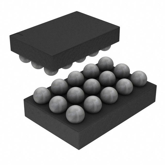


 工商网监
湘ICP备2023018690号
工商网监
湘ICP备2023018690号
