NCP6360
Mini Buck Converter for
RF Power Amplifiers
The NCP6360, a PWM synchronous step−down DC−to−DC
converter, is optimized for supplying RF Power Amplifiers (PAs) used
into 3G/4G wireless systems (Mobile/ Smart Phones, Phablets,
Tablets, ...) powered by single−cell Lithium−Ion batteries. The device
is able to deliver up to 800 mA. The output voltage is monitorable
from 0.6 V to 3.4 V by an analog control pin VCON. The analog
control allows dynamically optimizing the RF Power Amplifier’s
efficiency during a communication while for example in roaming
situation with as a benefit an increased talk time. Also at light load for
optimizing the DC−to−DC converter efficiency, the NCP6360 enters
automatically in a PFM mode and operates in a slower switching
frequency corresponding to a reduced quiescent current in regards to
the PWM mode for which the device operates at a switching frequency
of 6 MHz. Synchronous rectification offers improved system
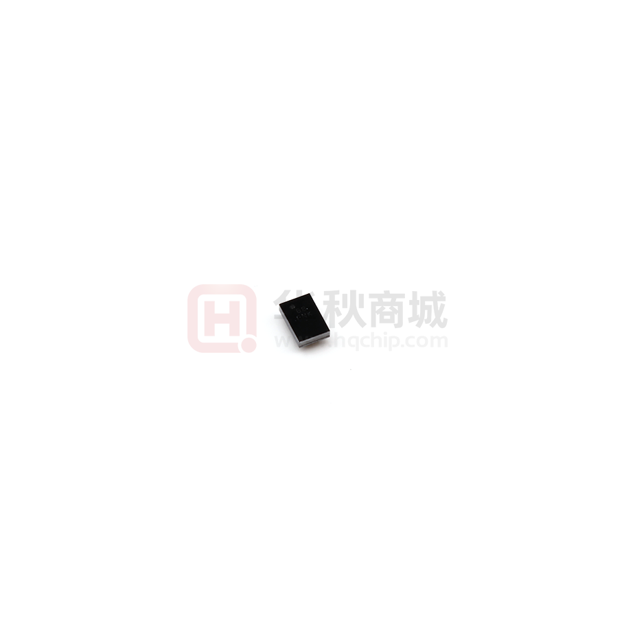
efficiency. The NCP6360 is available in a space saving, low profile
1.5 x 1.0 mm CSP−6 package.
www.onsemi.com
WLCSP6, 1.00x1.50
CASE 568AN
MARKING DIAGRAM
60
AYW
G
Features
•
•
•
•
•
•
•
•
•
Input Voltage from 2.7 V to 5.5 V for Battery Powered Applications
Adjustable Output Voltage (0.6 V to 3.4 V)
6 MHz Switching Frequency
Uses 470 nH Inductor and 4.7 mF Capacitor for Optimized Footprint
and Solution Thickness
PFM /PWM Automatic Mode Change for High Efficiency
Low 30 mA Quiescent Current
Thermal Protections to Avoid Damage of the IC
Small 1.5 x 1.0 mm / 0.5 mm Pitch CSP Package
This is a Pb−Free Device
A
Y
W
G
= Assembly Location
= Year
= Work Week
= Pb−Free Package
(Note: Microdot may be in either location)
ORDERING INFORMATION
See detailed ordering, marking and shipping information on
page 16 of this data sheet.
Typical Applications
• 3G / 4G Wireless Systems, Smart Phones, Phablets and Webtablets
NCP6360
VCON
FB
PVIN
Vout Control
Voltage control
From external DAC
10 mF
DCDC
Buck
Thermal
Protection
EN
DCDC Out
SW
1.0 A
6.0 MHz
0.47 mH
Enabling
Processor or
System Supply
VBAT
(Battery or System Supply)
PGND
4.7 mF
Rev 0.00
Figure 1. NCP6360 Block Diagram
© Semiconductor Components Industries, LLC, 2014
January, 2019 − Rev. 3
1
Publication Order Number:
NCP6360/D
�NCP6360
VBAT
NCP6360
DAC
VCON
PVIN
Vout Control
Voltage control
From external DAC
EN
Battery or
System Supply
10 uF
DCDC
Buck
Thermal
Protection
DCDC
Out
SW
1.0 A
6.0 MHz
Enabling
0.47 uH
4.7 uF
PGND
Modem
GPI/O
FB
RF TX
RF IN
RF OUT
3G/4G PAs
Power
Envelop
Detection
Figure 2. Typical Application
1.0 mm
A2
EN
PVIN
B1
B2
VCON
SW
C1
C2
FB
PGND
1.5 mm
A1
Figure 3. Pin Out (Top View)
www.onsemi.com
2
Coupler
Antenna
Switch
�NCP6360
PIN FUNCTION DESCRIPTION
Pin
Name
Type
A1
EN
Input
Description
A2
PVIN
Power
Input
B1
VCON
Input
B2
SW
Power
Output
DC−DC Switch Power. This pin connects the power transistors to one end of the inductor. Typical
application (6 MHz) uses 0.470 mH inductor; refer to application section for more information.
C1
FB
Power
Input
DC−DC Feedback Voltage. Must be connected to the output capacitor positive terminal. This is the
input of the error amplifier.
C2
PGND
Ground
DC−DC Power Ground. This pin is the power ground and carries high switching current. High
quality ground must be provided to prevent noise spikes. To avoid high−density current flow in a
limited PCB track, a local ground plane that connects all power grounds together is recommended.
Enable Control. Active high will enable the part. There is an internal pull down resistor on this pin.
DC−DC Power Supply. This pin must be decoupled to ground by a 10 mF and 1 mF ceramic
capacitors. These capacitors should be placed as close as possible to this pin.
Voltage Control Analog Input. This pin controls the output voltage. It must be shielded to protect
against noise. VOUT = 2.5 x VCON
MAXIMUM RATINGS
Rating
Symbol
Analog and power pins: PVIN, SW, FB
VCON pin
Digital pin: EN:
Input Voltage
Input Current
(Note 3)
Operating Ambient Temperature Range
Operating Junction Temperature Range (Note 1)
Value
Unit
VA
−0.3 to + 7.0
V
VVCON
−0.3 to + VA + 0.3 ≤ +7.0
V
VDG
IDG
−0.3 to VA +0.3 ≤ 7.0
10
V
mA
TA
−40 to +85
°C
TJ
−40 to +125
°C
Storage Temperature Range
TSTG
−65 to + 150
°C
Maximum Junction Temperature
TJMAX
−40 to +150
°C
Thermal Resistance Junction−to−Ambient (Note 2)
RqJA
85
°C/W
Electrostatic Discharge (ESD) Protection,
(Note 3)
HBM
CDM
2.0
1.5
kV
MSL
Level 1
Human Body Model
Charged Device Model
Moisture Sensitivity (Note 4)
Stresses exceeding those listed in the Maximum Ratings table may damage the device. If any of these limits are exceeded, device functionality
should not be assumed, damage may occur and reliability may be affected.
1. The thermal shutdown set to 165°C (typical) avoids potential irreversible damage on the device due to power dissipation.
2. The Junction−to−Ambient thermal resistance is a function of Printed Circuit Board (PCB) layout and application. This data is measured using
4−layer PCBs (2s2p). For a given ambient temperature TA it has to be pay attention to not exceed the max junction temperature TJMAX.
3. Human Body Model per JESD22−A114, Charge Device Model per JESD22−C101.
4. Moisture Sensitivity Level (MSL): 1 per IPC/JEDEC standard: J−STD−020A.
www.onsemi.com
3
�NCP6360
OPERATING CONDITIONS
Symbol
PVIN
L
Parameter
Conditions
Power Supply (Note 5)
Min
Typ
2.7
Inductor for DCDC converter (Note 6)
F = 6 MHz
Max
Unit
5.5
V
0.47
mH
Co
Output Capacitor for DCDC Converter (Note 6)
F = 6 MHz, L = 0.47 mH
4.7
−
33
mF
Co
Output Capacitor for DCDC Converter (Note 6)
F = 6 MHz, L = 0.33 mH
33
−
220
mF
Cin
Input Capacitor for DCDC Converter (Note 6)
4.7
10
mF
Functional operation above the stresses listed in the Recommended Operating Ranges is not implied. Extended exposure to stresses beyond
the Recommended Operating Ranges limits may affect device reliability.
5. Operation above 5.5 V input voltage for extended period may affect device reliability.
6. Including de−ratings (refer to application information section of this document for further details)
ELECTRICAL CHARACTERISTICS
Min and Max Limits apply for TJ up to +125°C unless otherwise specified. PVIN = 3.6 V (Unless otherwise noted). Typical values are
referenced to TA = + 25°C and default configuration
Parameter
Symbol
Conditions
Min
Typ
Max
Unit
SUPPLY CURRENT: PIN PVIN
IQ
Operating quiescent current
DCDC on – no load – no
switching, EN = High
TA = up to +85°C
PVIN = 2.7 V to 5.5 V
30
50
mA
ISLEEP
Product sleep mode current
PVIN = 5.5 V
VCON < 0.1 V, EN = High
TA = up to +85°C
25
60
mA
EN = Low
PVIN = 4.6 V
TA = up to +85°C
0.7
2.0
mA
5.5
V
IOFF
Product off current
DCDC CONVERTER
PVIN
Input Voltage Range (Note 7)
2.7
VOUT_MIN
Minimum Output Voltage (Note 8)
VCON = 0.24 V
0.55
0.6
0.65
V
VOUT_MAX
Maximum Output Voltage (Note 8)
VCON = 1.36 V
3.30
3.4
3.50
V
Gain
VOUT_ACC
FSW
VCON to VOUT Gain (Note 10)
2.5
VOUT Accuracy (Note 10)
Ideal = 2.5 x VCON
Switching Frequency (Note 9)
−50
−3
5.4
6.0
V/V
+50
+3
mV
%
6.6
MHz
RONHS
P−Channel MOSFET On Resistance
From PVIN to SW
168
mW
RONLS
N−Channel MOSFET On Resistance
From SW1 to PGND
78
mW
IPKHS
Peak Inductor Current PMOS
1.5
A
Maximum Duty Cycle (Note 10)
100
%
PVIN = 3.6 V, VOUT = 0.8 V
IOUT = 10 mA, PFM mode
82
%
PVIN = 3.6 V, VOUT = 1.8 V
IOUT = 300 mA, PWM mode
90
%
PVIN = 3.9 V, VOUT = 3.3 V
IOUT = 300 mA, PWM mode
94
%
DCMAX
h
Efficiency (Note 10)
Product parametric performance is indicated in the Electrical Characteristics for the listed test conditions, unless otherwise noted. Product
performance may not be indicated by the Electrical Characteristics if operated under different conditions.
7. Operation above 5.5 V input voltage for extended periods may affect device reliability.
8. Device tested under closed-loop conditions at PVIN = 4.0 V with VOUT_MIN and VOUT_MAX in line with VOUT accuracy specification.
9. Tested at 6 MHz / 48.
10. Guaranteed by design and characterized.
www.onsemi.com
4
�NCP6360
ELECTRICAL CHARACTERISTICS
Min and Max Limits apply for TJ up to +125°C unless otherwise specified. PVIN = 3.6 V (Unless otherwise noted). Typical values are
referenced to TA = + 25°C and default configuration
Symbol
Parameter
Conditions
Min
Typ
Max
Unit
DCDC CONVERTER
LINETR
Line Transient Response (Note 10)
PVIN = 3.6 V to 4.2 V
IOUT = 100 mA, VOUT = 0.8 V
TR = TF = 10 ms
50
mVpk
LOADTR
Load Transient Response (Note 10)
PVIN = 3.1 V / 3.6 V / 4.5 V
IOUT = 50 to 150 mA
TR = TF = 0.1 ms
50
mVpk
EN
VIH
Positive Going Input High Voltage
Threshold
VIL
Negative Going Input Low Voltage
Threshold
1.1
V
0.4
V
TOTAL DEVICE
IOUTMAX
TVCON
PWM mode (Note 10)
800
mA
VOUT step rise time from 0.6 V to 3.4 V
to reach 3.26 V (Note 10)
PVIN = 3.6 V, VOUT = 0.6 V to
3.4 V, COUT = 4.7 mF, RL = 10 W,
TR_VCON < 1 ms
25
ms
VOUT step fall time from 3.4 V to 0.6 V to
reach 0.74 V (Note 10)
PVIN = 3.6 V, VOUT = 3.4 V to
0.6 V, COUT = 4.7 mF, RL = 10 W,
TF_VCON < 1 ms
25
ms
TSTART
Soft−Start Time (Time from EN transitions from Low to High to 90% of Output
Voltage)
PVIN = 4.2 V, COUT = 4.7 mF,
VOUT = 3.4 V, no load
100
140
ms
TSP_en
Sleep mode Enter Time (Note 10)
Vcon < 75 mV
4.0
ms
TSP_ex
Sleep mode Exit Time (Note 10)
Vcon > 75 mV
5.0
ms
VUVLO
Under Voltage Lockout
PVIN falling
2.35
VUVLOH
Under Voltage Lockout Hysteresis
PVIN rising − PVIN falling
100
mV
2.5
V
TSD
Thermal Shut Down Protection
(Note 10)
155
°C
TSDH
Thermal Shut Down Hysteresis
(Note 10)
35
°C
Product parametric performance is indicated in the Electrical Characteristics for the listed test conditions, unless otherwise noted. Product
performance may not be indicated by the Electrical Characteristics if operated under different conditions.
7. Operation above 5.5 V input voltage for extended periods may affect device reliability.
8. Device tested under closed-loop conditions at PVIN = 4.0 V with VOUT_MIN and VOUT_MAX in line with VOUT accuracy specification.
9. Tested at 6 MHz / 48.
10. Guaranteed by design and characterized.
www.onsemi.com
5
�NCP6360
TYPICAL OPERATING CHARACTERISTICS
PVIN = EN = 3.6 V, L = 0.47 mH, COUT = 4.7 mF, CIN = 10 mF, Fsw = 6 MHz, TA = 25°C (unless otherwise noted)
Figure 4. Shutdown Current vs Input Voltage
(EN = Low, VCON = 0 V)
Figure 5. Shutdown Current vs Temperature
(EN = Low, VCON = 0 V)
TBD
Figure 6. Sleep Mode Current vs Input Voltage
(EN = High, VCON = 0 V, VOUT = 0 V)
Figure 7. Sleep Mode Current vs. Temperature
(EN = High, VCON = 0 V, VOUT = 0 V)
Figure 8. Quiescent Current vs Input Voltage
(EN = High, VCON = 0.8 V, VOUT = 2 V, no load)
Figure 9. Quiescent Current vs Temperature (TA)
(EN = High, VCON = 0.8 V, VOUT = 2 V, no load)
www.onsemi.com
6
�NCP6360
TYPICAL OPERATING CHARACTERISTICS
PVIN = EN = 3.6 V, L = 0.47 mH, COUT = 4.7 mF, CIN = 10 mF, Fsw = 6 MHz, TA = 25°C (unless otherwise noted)
Figure 11. VOUT Accuracy vs. Output Current vs.
Temperature PVIN = 3.6 V, VOUT = 0.8 V
Figure 10. VOUT Accuracy vs. Output
Current vs. PVIN @ 255C, VOUT = 0.8 V
Figure 12. VOUT Accuracy vs. Output
Current vs. PVIN @ 255C, VOUT = 1.8 V
Figure 13. VOUT Accuracy vs. Output Current
vs. Temperature PVIN = 3.6 V, VOUT = 1.8 V
Figure 14. VOUT Accuracy vs. Output
Current vs. PVIN @ 255C, VOUT = 3.3 V
Figure 15. VOUT Accuracy vs. Output Current
vs. Temperature PVIN = 4.2 V, VOUT = 3.3 V
www.onsemi.com
7
�NCP6360
TYPICAL OPERATING CHARACTERISTIC
PVIN = EN = 3.6 V, L = 0.47 mH, COUT = 4.7 mF, CIN = 10 mF, Fsw = 6 MHz, TA = 25°C (unless otherwise noted)
Figure 16. NMOS RDS(on) vs. PVIN
Figure 17. PMOS RDS(on) vs. PVIN
Figure 18. Efficiency vs. VOUT
RL = 6 W, Temp = 255C
Figure 19. Efficiency vs. VOUT
RL = 10 W, Temp = 255C
Figure 20. Efficiency vs. VOUT
RL = 22 W, Temp = 255C
www.onsemi.com
8
�NCP6360
TYPICAL OPERATING CHARACTERISTICS
PVIN = EN = 3.6 V, L = 0.47 mH, COUT = 4.7 mF, CIN = 10 mF, Fsw = 6 MHz, TA = 25°C (unless otherwise noted)
Figure 22. Efficiency vs. Output Current
VOUT = 0.8 V, VIN = 3.6 V
Figure 21. Efficiency vs. Output Current
VOUT = 0.8 V, Temp = 255C
Figure 23. Efficiency vs. Output Current
VOUT = 1.8 V, Temp = 255C
Figure 24. Efficiency vs. Output Current
VOUT = 1.8 V, VIN = 3.6 V
Figure 25. Efficiency vs. Output Current
VOUT = 3.3 V, Temp = 255C
Figure 26. Efficiency vs. Output Current
VOUT = 3.3 V, VIN = 4.2 V
www.onsemi.com
9
�NCP6360
TYPICAL OPERATING CHARACTERISTICS
PVIN = EN = 3.6 V, L = 0.47 mH, COUT = 4.7 mF, CIN = 10 mF, Fsw = 6 MHz, TA = 25°C (unless otherwise noted)
Figure 27. 6 MHz, Switching Frequency
vs. Temperature (TA)
Figure 28. Transient, VOUT vs. VCON, RL = 10 W,
VOUT = 0.4 V to 3.6 V, PVIN = 3.9 V w/ TR = 7 ms,
TF = 10 ms
Figure 29. Output Voltage Waveforms in
PFM Mode IOUT = 100 mA, PVIN = 3.6 V,
VOUT = 2.5 V, COUT = 4.7 mF
Figure 30. Output Voltage Waveforms in PFM
Mode IOUT = 100 mA, PVIN = 3.6 V, VOUT = 2.5 V,
COUT = 2 x 4.7 mF
Figure 31. Line Transient Response < 20 mV
Peak, PVIN = 3.6 V to 4.1 V, RL = 8 W, VOUT = 1.8 V
Figure 32. Load Transient Response w/ DVmeas <
50 mV Peak, IOUT = 50 to 150 mA, VOUT = 2.5 V
www.onsemi.com
10
�NCP6360
TYPICAL OPERATING CHARACTERISTICS
PVIN = EN = 3.6 V, L = 0.47 mH, COUT = 4.7 mF, CIN = 10 mF, Fsw = 6 MHz, TA = 25°C (unless otherwise noted)
Figure 33. Load Transient Response w/ DVmeas <
50 mV Peak, IOUT = 10 to 60 mA, VOUT = 2.5 V
Figure 34. Power−up Transient Response
PVIN = 4.2 V, VOUT = 3.4 V, RL = 2.5 kW
Figure 35. Power−up Transient Response
PVIN = 4.2 V, VOUT = 3.4 V, RL = 10 W
Figure 36. Power−down Transient Response
PVIN = 4.2 V, VOUT = 3.4 V, RL = 10 W
www.onsemi.com
11
�NCP6360
OPERATING DESCRIPTION
General Description
synchronous converter provides a lower voltage drop than
the diode in an asynchronous converter, which provides less
loss and higher efficiency.
The NCP6360 is a voltage−mode standalone synchronous
step−down DC−to−DC converter designed to supply RF
Power Amplifiers (PAs) used into 3G/4G wireless systems
(Mobile/ Smart Phones, Phablets, Tablets, ...) powered by
single−cell Lithium−Ion batteries. The IC can deliver up to
800 mA when operating in PWM mode.
The buck converter output voltage ranging from 0.6 V to
3.4 V can be monitored by the system’s PA output RF power
through the control pin VCON. The control voltage range is
from 0.24 V to 1.36 V and Vout is equal to 2.5 times this
control voltage. VCON allows the PA to have its efficiency
dynamically optimized during communication calls in the
case for example of roaming situation involving a constant
adjustment of the PA output power. The value−added benefit
is an increase of the absolute talk time.
Synchronous rectification and automatic PFM/PWM
operating mode transitions improve overall solution
efficiency. The device operates at 6 MHz switching
frequency.
PFM (Pulse Frequency Modulation) Operating Mode
In order to save power and improve efficiency at low loads
the NCP6360 operates in PFM mode as the inductor drops
into DCM (Discontinuous Current Mode). The upper FET
on time is kept constant and the switching frequency is
variable. Output voltage is regulated by varying the
switching frequency which becomes proportional to loading
current. As it does in PWM mode, the internal N−MOSFET
operates as synchronous rectifier after each P−MOSFET
on−pulse. When load increases and current in inductor
becomes continuous again, the controller automatically
turns back to PWM mode.
Sleep Mode
The NCP6360 device enters the sleep mode in about 4ms
when the control voltage VCON goes below typically
70 mV. Vout is extremely low, close to 0 V and in a state out
of regulation. In this Vout condition the Sleep mode enables
a low current state (40 mA typical range). The buck
converter exits the sleep mode and returns in a regulation
state when VCON goes above 110 mV after typically 5 ms.
Buck DC−to−DC Converter Operating
The converter is a synchronous rectifier type with both
high side and low side integrated switches. Neither external
transistor nor diodes are required for NCP6360 operation.
Feedback and compensation network are also fully
integrated. The device can operate in four different modes:
shutdown mode (EN = Low, device off), Sleep Mode when
VCON below about 0.1 V, PFM mode for efficiency
optimization purpose when operating at light load and PWM
mode when operating in medium and high loads. The
transitions between PWM and PFM modes occur
automatically.
Inductor Peak Current limitations
During normal operation, peak current limitation will
monitor and limit the current through the inductor. This
current limitation is particularly useful when size and/or
height constrain inductor power. The High Side Switch
(HSS) peak current limitation is typically 1.5 A, while the
Low Side Switch (LSS) has a peak current up to 0.8 A. The
HSS peak current contributes to limit the current during soft
start sequence in high load conditions.
Shutdown Mode
The NCP6360 enters shutdown mode when setting the EN
pin Low (below 0.4 V) or when PVIN drops below its
UVLO threshold value (2.35 V typical). In shutdown mode,
the internal reference, oscillator and most of the control
circuitries are turned off. The typical current consumption is
0.7 mA. Applying a voltage above 1.1 V to EN pin will
enable the device for normal operation. A soft−start
sequence is run when activating EN high. EN pin should be
activated after the input voltage is applied.
Under−voltage Lockout (UVLO)
NCP6360 core does not operate for voltages below the
Under Voltage lock Out (UVLO) level. Below UVLO
threshold (typical 2.35 V), all internal circuitry (both analog
and digital) is held in reset. NCP6360 operation is not
guaranteed down to VUVLO when battery voltage is
dropping off. To avoid erratic on / off behavior,a typical
100 mV hysteresis is implemented. Restart is guaranteed at
2.6 V when VBAT voltage is recovering or rising.
PWM (Pulse Width Modulation) Operating Mode
Power−Up / Power−Down Sequencing
In medium and high load conditions, the NCP6360
operates in PWM mode from a fixed clock (6 MHz) and
adapts its duty cycle to regulate the desired output voltage.
In this mode, the inductor current is in CCM (Continuous
Current Mode) and the voltage is regulated by PWM. The
internal N−MOSFET switch operates as synchronous
rectifier and is driven complementary to the P−MOSFET
switch. In CCM, the lower switch (N−MOSFET) in a
The EN pin controls NCP6360 start up. EN pin Low to
High transition starts the power up sequencer which is
combined with a soft start consisting to limit the inrush
current at 800 mA while the output voltage is establishing.
If EN is made low, the DC to DC converter is turned off and
device enters shutdown mode.
A built−in pull−down resistor disables the device when
this pin is left unconnected or not driven.
www.onsemi.com
12
�NCP6360
PVIN
Rising UVLO < 2.6 V
POR
EN
VOUT
IOUT
HSS Ipeak
Soft Start 800mA
Wake Up Time ~ TBD
Figure 37. Power−Up Sequence
IC from damage. This protection circuitry is only activated
when the core is in active mode (output voltage is turned on).
During thermal shut down, output voltage is turned off and
the device enters sleep mode.
Thermal shut down threshold is set at 155°C (typical)
when the die temperature increases and, in order to avoid
erratic on / off behavior, a 35°C hysteresis is implemented.
So, after a typical 155°C thermal shut down, the NCP6360
will return to normal operation when the die temperature
cools to 120°C. This normal operation depends on the input
conditions and configuration at the time the device recovers.
In order to power up the circuit, the input voltage PVIN
has to rise above the UVLO threshold (Rising UVLO). This
triggers the internal core circuitry power up which is the
“Wake Up Time” (including “Bias Time”).
This delay is internal and cannot be bypassed.
The power down sequence is triggered by setting Low the
EN pin. The output voltage goes down to 0 V.
Thermal Shutdown Feature (TSD)
The thermal capability of IC can be exceeded due to step
down converter output stage power level. A thermal
protection circuitry is therefore implemented to prevent the
www.onsemi.com
13
�NCP6360
APPLICATION INFORMATION
VBAT
NCP6360
VCON
DAC
PVIN
Vout Control
Voltage control
From external DAC
Thermal
Protection
EN
Battery or
System Supply
10 uF
DCDC
Buck
DCDC
Out
SW
1.0 A
6.0 MHz
0.47 uH
4.7 uF
Enabling
PGND
Modem
GPI/O
FB
RF IN
RF TX
Antenna
Switch
Coupler
RF OUT
3G/4G PAs
Power
Envelop
Detection
Figure 38. Typical Application Schematic
Output Filter Design Considerations
50% of the maximum output current IOUTMAX for a
trade−off between transient response and output ripple. The
selected inductor must have high enough saturation current
rating to be higher than the maximum peak current that is:
The output filter introduces a double pole in the system at
a frequency of:
f LC +
1
2 @ p @ ǸL @ C
(eq. 1)
I LMAX + I OUTMAX )
The NCP6360 internal compensation network is
optimized for a typical output filter comprising a 470 nH
inductor and one 4.7 mF capacitor as described in the basic
application schematic Figure 38.
I LPP
(eq. 2)
2
The inductor also needs to have high enough current
rating based on temperature rise concern. Low DCR is good
for efficiency improvement and temperature rise reduction.
Tables 1 shows recommended inductor references.
Inductor Selection
The inductance of the inductor is determined by given
peak−to−peak ripple current ILPP of approximately 20% to
Table 1. RECOMMENDED INDUCTORS WHEN OPERATING AT 6 MHz
Supplier
Part#
Value (mH)
Size (L x l x T) (mm)
DC Rated Current (A)
DCR Max @ 255C (mW)
TDK
TFM201610A−R47M−T00
0.47
2.0 x 1.6 x 1.0
3.5
46
TDK
TFM201210A−R47M−T00
0.47
2.0 x 1.2 x 1.0
2.5
65
Toko
DFE201610R−R47M−T00
0.47
2.0 x 1.6 x 1.0
3.8
48
Toko
DFE201610A−R47M−T00
0.47
2.0 x 1.6 x 1.0
3.7
58
www.onsemi.com
14
�NCP6360
Output Capacitor Selection
ripple and get better decoupling in the input power supply
rail, ceramic capacitor is recommended due to low ESR and
ESL. The minimum input capacitance regarding the input
ripple voltage VINPP is
The output capacitor selection is determined by output
voltage ripple and load transient response requirement. For
high transient load performance high output capacitor value
must be used. For a given peak−to−peak ripple current ILPP
in the inductor of the output filter, the output voltage ripple
across the output capacitor is the sum of three components
as below.
C INMIN +
D+
(eq. 3)
Where VOUTPP(C) is the ripple component coming from
an equivalent total capacitance of the output capacitors,
VOUTPP(ESR) is a ripple component from an equivalent ESR
of the output capacitors, and VOUTPP(ESL) is a ripple
component from an equivalent ESL of the output capacitors.
In PWM operation mode, the three ripple components can
be obtained by
I L_PP
8 @ C @ f SW
V OUTPP(ESR) + I LPP @ ESR
V OUT_PP(ESL) +
ESL
ESL ) L
@ V IN
ǒPV IN * VOUTǓ @ VOUT
PV IN @ F SW @ L
I LPP
8 @ V OUTPP @ f SW
V OUT
V IN
I INRMS + I OUTMAX @ ǸD * D 2
(eq. 10)
(eq. 11)
The input capacitor needs also to be sufficient to protect
the device from over voltage spike and a minimum of 4.7 mF
capacitor is required. The input capacitor should be located
as close as possible to the IC. PGND is connected to the
ground terminal of the input cap which then connects to the
ground plane. The PVIN is connected to the VBAT terminal
of the input capacitor which then connects to the VBAT
plane.
(eq. 4)
(eq. 5)
(eq. 6)
Layout and PCB Design Recommendations
Good PCB layout helps high power dissipation from a
small package with reduced temperature rise. Thermal
layout guidelines are:
• A four or more layers PCB board with solid ground
planes is preferred for better heat dissipation.
• More free vias are welcome to be around IC to connect
the inner ground layers to reduce thermal impedance.
• Use large area copper especially in top layer to help
thermal conduction and radiation.
• Use two layers for the high current paths (PVIN,
PGND, SW) in order to split current in two different
paths and limit PCB copper self heating.
(eq. 7)
In applications with all ceramic output capacitors, the
main ripple component of the output ripple is VOUTPP(C).
So that the minimum output capacitance can be calculated
regarding to a given output ripple requirement VOUTPP in
PWM operation mode.
C MIN +
(eq. 9)
In addition the input capacitor needs to be able to absorb
the input current, which has a RMS value of:
And the peak−to−peak ripple current is:
I LPP +
V INPP @ f SW
Where
V OUTPP + V OUTPP(C) ) V OUTPP(ESR) ) V OUTPP(ESL)
V OUTPP(C) +
I OUTMAX @ ǒD * D 2Ǔ
(eq. 8)
(See demo board example Figure 40)
Input Capacitor Selection
One of the input capacitor selection guides is the input
voltage ripple requirement. To minimize the input voltage
www.onsemi.com
15
�NCP6360
3.60 mm
0402
SW
FB
PGND
2.0 x 1.2 mm
VCON
0402
PVIN
1.5 x 0.9 mm
EN
2.80 mm
TFM201210
1.5 x 0.9 mm
S < 10.1 mm@
Figure 39. Layout Minimum Recommended Occupied Space Using 0402 Capacitors and 0805
(2.0 x 1.2 x 1.0 mm) Inductor
Input capacitor placed as close as possible to the IC.
• PVIN directly connected to Cin input capacitor, and
then connected to the Vin plane. Local mini planes used
on the top layer (green) and layer just below top layer
with laser vias.
• PGND directly connected to Cin input capacitor, and
then connected to the GND plane: Local mini planes
•
used on the top layer (green) and layer just below top
layer with laser vias.
SW connected to the Lout inductor with local mini
planes used on the top layer (green) and layer just
below top layer with laser vias.
Figure 40. Example of PCB Implementation
(PCB case with 0805 (2.0 x 1.2 mm) Capacitors and 2016 (2.0 x 1.6 x 1.0 mm) Inductors
ORDERING INFORMATION
Device
NCP6360FCCT2G
Package
Shipping†
WLCSP6
(Pb−Free)
3000 / Tape & Reel
†For information on tape and reel specifications, including part orientation and tape sizes, please refer to our Tape and Reel Packaging
Specifications Brochure, BRD8011/D.
www.onsemi.com
16
�MECHANICAL CASE OUTLINE
PACKAGE DIMENSIONS
WLCSP6, 1.00x1.50x0.592
CASE 568AN
ISSUE C
DATE 28 JUN 2022
GENERIC
MARKING DIAGRAM*
XXX
AYW
G
A
Y
W
G
= Assembly Location
= Year
= Work Week
= Pb−Free Package
*This information is generic. Please refer to
device data sheet for actual part marking.
Pb−Free indicator, “G” or microdot “G”, may
or may not be present. Some products may
not follow the Generic Marking.
DOCUMENT NUMBER:
DESCRIPTION:
98AON81730F
WLCSP6, 1.00X1.50X0.592
Electronic versions are uncontrolled except when accessed directly from the Document Repository.
Printed versions are uncontrolled except when stamped “CONTROLLED COPY” in red.
PAGE 1 OF 1
onsemi and
are trademarks of Semiconductor Components Industries, LLC dba onsemi or its subsidiaries in the United States and/or other countries. onsemi reserves
the right to make changes without further notice to any products herein. onsemi makes no warranty, representation or guarantee regarding the suitability of its products for any particular
purpose, nor does onsemi assume any liability arising out of the application or use of any product or circuit, and specifically disclaims any and all liability, including without limitation
special, consequential or incidental damages. onsemi does not convey any license under its patent rights nor the rights of others.
© Semiconductor Components Industries, LLC, 2019
www.onsemi.com
�onsemi,
, and other names, marks, and brands are registered and/or common law trademarks of Semiconductor Components Industries, LLC dba “onsemi” or its affiliates
and/or subsidiaries in the United States and/or other countries. onsemi owns the rights to a number of patents, trademarks, copyrights, trade secrets, and other intellectual property.
A listing of onsemi’s product/patent coverage may be accessed at www.onsemi.com/site/pdf/Patent−Marking.pdf. onsemi reserves the right to make changes at any time to any
products or information herein, without notice. The information herein is provided “as−is” and onsemi makes no warranty, representation or guarantee regarding the accuracy of the
information, product features, availability, functionality, or suitability of its products for any particular purpose, nor does onsemi assume any liability arising out of the application or use
of any product or circuit, and specifically disclaims any and all liability, including without limitation special, consequential or incidental damages. Buyer is responsible for its products
and applications using onsemi products, including compliance with all laws, regulations and safety requirements or standards, regardless of any support or applications information
provided by onsemi. “Typical” parameters which may be provided in onsemi data sheets and/or specifications can and do vary in different applications and actual performance may
vary over time. All operating parameters, including “Typicals” must be validated for each customer application by customer’s technical experts. onsemi does not convey any license
under any of its intellectual property rights nor the rights of others. onsemi products are not designed, intended, or authorized for use as a critical component in life support systems
or any FDA Class 3 medical devices or medical devices with a same or similar classification in a foreign jurisdiction or any devices intended for implantation in the human body. Should
Buyer purchase or use onsemi products for any such unintended or unauthorized application, Buyer shall indemnify and hold onsemi and its officers, employees, subsidiaries, affiliates,
and distributors harmless against all claims, costs, damages, and expenses, and reasonable attorney fees arising out of, directly or indirectly, any claim of personal injury or death
associated with such unintended or unauthorized use, even if such claim alleges that onsemi was negligent regarding the design or manufacture of the part. onsemi is an Equal
Opportunity/Affirmative Action Employer. This literature is subject to all applicable copyright laws and is not for resale in any manner.
PUBLICATION ORDERING INFORMATION
LITERATURE FULFILLMENT:
Email Requests to: orderlit@onsemi.com
onsemi Website: www.onsemi.com
◊
TECHNICAL SUPPORT
North American Technical Support:
Voice Mail: 1 800−282−9855 Toll Free USA/Canada
Phone: 011 421 33 790 2910
Europe, Middle East and Africa Technical Support:
Phone: 00421 33 790 2910
For additional information, please contact your local Sales Representative
�


 工商网监
湘ICP备2023018690号
工商网监
湘ICP备2023018690号

