NCP81156
Product Preview
MOSFET Driver
The NCP81156 is a high−performance dual MOSFET gate driver in
a small 2 mm x 2 mm package, optimized to drive the gates of both
high−side and low−side power MOSFETs in a buck or buck−boost
application. VCC UVLO ensures the MOSFETs are off when supply
voltages are low. A bi−directional Enable pin provides a fault signal to
the controller when a UVLO fault is detected.
www.onsemi.com
MARKING
DIAGRAM
Features
•
•
•
•
•
•
•
•
•
Space−Efficient 2 mm x 2 mm DFN8 Thermally−Enhanced Package
VCC Range of 4.5 V to 13.2 V
Integrated Bootstrap Diode
Compatible with 3.3 V and 5 V PWM Inputs
Bi−Directional Enable Feature Pulls Enable Pin low during a UVLO
Fault.
Adaptive Anti−Cross Conduction Circuit Protects against
Cross−Conduction during FET Turn−on and Turn−off
Output Disable Control Turns Off Both MOSFETs
VCC Under−voltage Lockout
These Devices are Pb−Free, Halogen Free/BFR Free and are RoHS
Compliant
Typical Applications
• E−Cigarettes
• Unmanned Aerial Vehicles (UAV)
1
1
DFN8
MN SUFFIX
CASE 506AA
EYMG
G
EY = Specific Device Code
M = Date Code
G
= Pb−Free Package
(Note: Microdot may be in either location)
PINOUT DIAGRAM
BST
1
PWM
2
EN
3
VCC
4
This document contains information on a product under development. ON Semiconductor
reserves the right to change or discontinue this product without notice.
FLAG
9
8
DRVH
7
SW
6
GND
5
DRVL
(Top View)
ORDERING INFORMATION
Device
Package
Shipping†
NCP81156MNTBG
DFN8
(Pb−Free)
3000 / Tape &
Reel
†For information on tape and reel specifications,
including part orientation and tape sizes, please
refer to our Tape and Reel Packaging Specifications
Brochure, BRD8011/D.
© Semiconductor Components Industries, LLC, 2018
July, 2018 − Rev. P0
1
Publication Order Number:
NCP81156/D
�NCP81156
12V_POWER
Figure 1. Typical Application Schematic
BST
VCC
DRVH
PWM
Logic
SW
Anti-Cross
Conduction
VCC
DRVL
EN
VCC
UVLO
Fault
Figure 2. Simplified Block Diagram
www.onsemi.com
2
�NCP81156
Table 1. PIN FUNCTION DESCRIPTION
Pin No.
Symbol
Description
1
BST
Bootstrap supply voltage. Connect a MLCC capacitor of at least 0.1mF from this pin to SW.
2
PWM
Two−state Input.
3
EN
Enable Input.
4
VCC
5.0 V power supply for the control logic circuit.
5
DRVL
Low−side gate drive output. Connect to the gate of low−side MOSFET.
6
GND
Analog Ground.
7
SW
8
DRVH
High−side gate drive output. Connect to the gate of high−side MOSFET.
9
FLAG
Thermal Flag. Connect to ground plane.
Switch−node Output.
Table 2. ABSOLUTE MAXIMUM RATINGS (Electrical Information − all signals referenced to GND unless noted otherwise.)
Pin Symbol
Pin Name
VMAX
VMIN
VCC
Main Supply Voltage Input
15 V
16 V (< 50 ns)
−0.3 V
BST
Bootstrap Supply Voltage
35 V wrt/ GND
40 V ≤ 50 ns wrt/ GND 15 V wrt/ SW
−0.3 V wrt/SW
SW
Switching Node (Bootstrap Supply
Return)
35 V
40 V ≤ 50 ns
−5 V
−10 V (200 ns)
DRVH
High Side Driver Output
BST+0.3 V
SW + 15 V (< 80 ns)
−0.3 V wrt/SW
−2 V (
很抱歉,暂时无法提供与“NCP81156MNTBG”相匹配的价格&库存,您可以联系我们找货
免费人工找货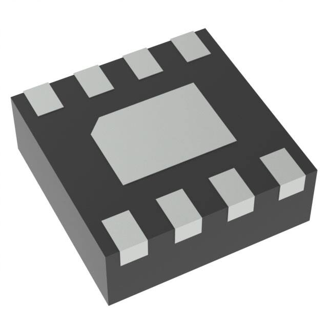


 工商网监
湘ICP备2023018690号
工商网监
湘ICP备2023018690号
