NCV4264-2C
Linear Regulator,
Low Dropout, Low IQ
The NCV4264−2C is a low quiescent current consumption LDO
regulator. Its output stage supplies 100 mA with ±2.0% output
voltage accuracy.
Maximum dropout voltage is 500 mV at 100 mA load current.
It is internally protected against 45 V input transients, input supply
reversal, output overcurrent faults, and excess die temperature. No
external components are required to enable these features.
www.onsemi.com
MARKING
DIAGRAM
TAB
Features
•
•
•
•
•
•
•
•
3.3 V and 5.0 V Fixed Output
±2.0% Output Accuracy, Over Full Temperature Range
33 mA Typical Quiescent Current
500 mV Maximum Dropout Voltage at 100 mA Load Current
Wide Input Voltage Operating Range of 4.5 V to 45 V
Internal Fault Protection
♦ −42 V Reverse Voltage
♦ Short Circuit/Overcurrent
♦ Thermal Overload
NCV Prefix for Automotive and Other Applications Requiring
Unique Site and Control Change Requirements; AEC−Q100
Qualified and PPAP Capable
This is a Pb−Free Device
1 2
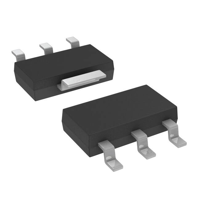
SOT−223
ST SUFFIX
CASE 318E
3
AYW
642CxG
G
1
x
= 5 (5.0 V Version)
= 3 (3.3 V Version)
= Assembly Location
= Year
= Work Week
= Pb−Free Package
A
Y
W
G
(Note: Microdot may be in either location)
PIN CONNECTIONS
TAB
1
VIN GND VOUT
(Top View)
ORDERING INFORMATION
See detailed ordering and shipping information in the package
dimensions section on page 9 of this data sheet.
© Semiconductor Components Industries, LLC, 2015
November, 2018 − Rev. 3
1
Publication Order Number:
NCV4264−2C/D
�NCV4264−2C
VIN
VOUT
1.3 V
Reference
+
Error
Amp
-
Thermal
Shutdown
GND
Figure 1. Block Diagram
PIN FUNCTION DESCRIPTION
Pin No.
Symbol
Function
1
VIN
2
GND
Ground; substrate.
3
VOUT
Regulated output voltage; collector of the internal PNP pass transistor.
TAB
GND
Ground; substrate and best thermal connection to the die.
Unregulated input voltage; 4.5 V to 45 V.
OPERATING RANGE
Rating
Symbol
Min
Max
Unit
VIN, DC Input Operating Voltage (Note 3)
VIN
4.5
+45
V
Junction Temperature Operating Range
TJ
−40
+150
°C
Functional operation above the stresses listed in the Recommended Operating Ranges is not implied. Extended exposure to stresses beyond the
Recommended Operating Ranges limits may affect device reliability.
MAXIMUM RATINGS
Rating
VIN, DC Input Voltage
VOUT, DC Voltage
Symbol
Min
Max
Unit
VIN
−42
+45
V
VOUT
−0.3
+32
V
Storage Temperature
Tstg
−55
+150
°C
Moisture Sensitivity Level
MSL
3
−
ESD Capability, Human Body Model (Note 1)
VESDHB
4000
−
V
ESD Capability, Machine Model (Note 1)
VESDMIM
200
−
V
−
265 pk
Lead Temperature Soldering
Reflow (SMD Styles Only), Lead Free (Note 2)
Tsld
°C
Stresses exceeding those listed in the Maximum Ratings table may damage the device. If any of these limits are exceeded, device functionality
should not be assumed, damage may occur and reliability may be affected.
1. This device series incorporates ESD protection and is tested by the following methods:
ESD HBM tested per AEC−Q100−002 (EIA/JESD22−A 114C)
ESD MM tested per AEC−Q100−003 (EIA/JESD22−A 115C)
2. Lead Free, 60 sec – 150 sec above 217°C, 40 sec max at peak.
3. See specific conditions for DC operating input voltage lower than 4.5 V in ELECTRICAL CHARACTERISTICS table at page 3
www.onsemi.com
2
�NCV4264−2C
THERMAL RESISTANCE
Parameter
Symbol
Min
Max
Unit
°C/W
Junction−to−Ambient
SOT−223
RqJA
−
109 (Note 4)
Junction−to−Tab (psi−JL4)
SOT−223
YJL4
−
10.9
ELECTRICAL CHARACTERISTICS (VIN = 13.5 V, TJ = −40°C to +150°C, unless otherwise noted.)
Characteristic
Symbol
Test Conditions
Min
Typ
Max
Unit
Output Voltage
5.0 V Version
VOUT
5.0 mA v IOUT v 100 mA (Note 5)
6.0 V v VIN v 28 V
4.900
5.0
5.100
V
Output Voltage
3.3 V Version
VOUT
5.0 mA v IOUT v 100 mA (Note 5)
4.5 V v VIN v 28 V
3.234
3.3
3.366
V
Output Voltage
3.3 V Version
VOUT
IOUT = 5 mA, VIN = 4 V (Note 7)
3.234
3.3
3.366
V
Line Regulation
5.0 V Version
DVOUT vs. VIN
IOUT = 5.0 mA
6.0 V v VIN v 28 V
−30
0.7
+30
mV
Line Regulation
3.3 V Version
DVOUT vs. VIN
IOUT = 5.0 mA
4.5 V v VIN v 28 V
−30
0.57
+30
mV
Load Regulation
DVOUT vs. IOUT
1.0 mA v IOUT v 100 mA (Note 5)
−40
0.6
+40
mV
VIN−VOUT
IOUT = 100 mA (Notes 5 & 6)
−
230
500
mV
Iq
IOUT = 100 mA
TJ = 25°C
TJ = −40°C to +85°C
TJ = −40°C to 150°C
−
−
−
33
33
33
55
60
70
Active Ground Current
IG(ON)
IOUT = 50 mA (Note 5)
−
0.55
4.0
mA
Power Supply Rejection
PSRR
VRIPPLE = 0.5 VP−P, F = 100 Hz
−
67
−
dB
Current Limit
IOUT(LIM)
VOUT = 4.5 V (5.0 V Version) (Note 5)
VOUT = 3.0 V (3.3 V Version) (Note 5)
150
150
−
−
500
500
mA
Short Circuit Current Limit
IOUT(SC)
VOUT = 0 V (Note 5)
40
−
500
mA
TTSD
(Note 7)
150
−
200
°C
Dropout Voltage − 5.0 V Version
Quiescent Current
mA
PROTECTION
Thermal Shutdown Threshold
Product parametric performance is indicated in the Electrical Characteristics for the listed test conditions, unless otherwise noted. Product
performance may not be indicated by the Electrical Characteristics if operated under different conditions.
4. 1 oz., 100 mm2 copper area.
5. Use pulse loading to limit power dissipation.
6. Dropout voltage = (VIN–VOUT), measured when the output voltage has dropped 100 mV relative to the nominal value obtained with
VIN = 13.5 V.
7. Not tested in production. Limits are guaranteed by design.
4.5−45 V
Input
Vin
CIN
100 nF
1
4264−2C
3
Vout
2
GND
Figure 2. Applications Circuit
www.onsemi.com
3
Output
COUT
10 mF
�NCV4264−2C
TYPICAL CHARACTERISTIC CURVES − 5 V Version
100
Unstable Region
ESR (W)
10
1
Stable Region
0.1
COUT ≥ 10 mF
0.01
0
10
30
20
50
40
60
70
90
80
100
IOUT, OUTPUT CURRENT (mA)
Figure 3. Output Stability with Output
Capacitor ESR (5.0 V Version)
6
5.00
4.95
VIN = 13.5 V
RL = 1 kW
4.90
−40
0
80
40
120
3
2
RL = 50 W
TJ = 25°C
1
0
160
0
1
2
3
5
4
7
6
8
9
Figure 4. Output Voltage vs. Junction
Temperature (5.0 V Version)
Figure 5. Output Voltage vs. Input Voltage
(5.0 V Version)
300
TJ = 25°C
250
200
TJ = −40°C
150
100
50
25
50
75
100
125
10
350
TJ = 125°C
0
4
VIN, INPUT VOLTAGE (V)
350
0
5
TJ, JUNCTION TEMPERATURE (°C)
400
VDR, DROPOUT VOLTAGE (mV)
VOUT, OUTPUT VOLTAGE (V)
5.05
IOUT, OUTPUT CURRENT (mA)
VOUT, OUTPUT VOLTAGE (V)
5.10
300
250
200
150
100
50
0
150
VOUT = 0 V
TJ = 25°C
0
5
10
15
20
25
30
35
40
IOUT, OUTPUT CURRENT (mA)
VIN, INPUT VOLTAGE (V)
Figure 6. Dropout Voltage vs. Output Current
(only 5.0 V Version)
Figure 7. Maximum Output Current vs. Input
Voltage (5.0 V Version)
www.onsemi.com
4
45
�NCV4264−2C
100
3.5
90
Iq, QUIESCENT CURRENT (mA)
4.0
VIN = 13.5 V
TJ = 25°C
3.0
2.5
2.0
1.5
1.0
0.5
0
0
50
100
150
VIN = 13.5 V
TJ = 25°C
80
70
60
50
40
30
20
10
0
0
1
2
3
4
IOUT, OUTPUT CURRENT (mA)
IOUT, OUTPUT CURRENT (mA)
Figure 8. Quiescent Current vs. Output Current
(5.0 V Version) (High Load)
Figure 9. Quiescent Current vs. Output Current
(5.0 V Version) (Low Load)
4.0
Iq, QUIESCENT CURRENT (mA)
Iq, QUIESCENT CURRENT (mA)
TYPICAL CHARACTERISTIC CURVES − 5 V Version
3.5
TJ = 25°C
3.0
2.5
RL = 50 W
2.0
1.5
1.0
RL = 100 W
0.5
0
0
5
10
15
20
25
30
35
VIN, INPUT VOLTAGE (V)
Figure 10. Quiescent Current vs. Input Voltage
(5.0 V Version)
www.onsemi.com
5
40
5
�NCV4264−2C
TYPICAL CHARACTERISTIC CURVES − 3.3 V Version
100
Unstable Region
ESR (W)
10
1
Stable Region
0.1
COUT ≥ 10 mF
0.01
0
10
20
30
50
40
70
60
80
100
90
IOUT, OUTPUT CURRENT (mA)
Figure 11. Output Stability with Output
Capacitor ESR (3.3 V Version)
4
VOUT, OUTPUT VOLTAGE (V)
VOUT, OUTPUT VOLTAGE (V)
3.36
3.34
3.32
3.30
3.28
VIN = 13.5 V
RL = 660 W
3.26
3.24
−40
0
40
80
120
RL = 33 W
TJ = 25°C
1
0
1
2
3
4
5
6
7
8
9
TJ, JUNCTION TEMPERATURE (°C)
VIN, INPUT VOLTAGE (V)
Figure 12. Output Voltage vs. Junction
Temperature (3.3 V Version)
Figure 13. Output Voltage vs. Input Voltage
(3.3 V Version)
10
2.0
Iq, QUIESCENT CURRENT (mA)
IOUT, OUTPUT CURRENT (mA)
2
0
160
350
300
250
200
150
100
VOUT = 0 V
TJ = 25°C
50
0
3
0
5
10
15
20
25
30
35
40
45
1.8
TJ = 25°C
1.6
1.4
1.2
RL = 50 W
1.0
0.8
0.6
RL = 100 W
0.4
0.2
0
0
5
10
15
20
25
30
35
40
VIN, INPUT VOLTAGE (V)
VIN, INPUT VOLTAGE (V)
Figure 14. Maximum Output Current vs. Input
Voltage (3.3 V Version)
Figure 15. Quiescent Current vs. Input Voltage
(3.3 V Version)
www.onsemi.com
6
�NCV4264−2C
4.0
100
3.5
90
Iq, QUIESCENT CURRENT (mA)
Iq, QUIESCENT CURRENT (mA)
TYPICAL CHARACTERISTIC CURVES − 3.3 V Version
3.0
2.5
2.0
1.5
1.0
VIN = 13.5 V
TJ = 25°C
0.5
0
0
50
100
150
80
70
60
50
40
30
20
10
0
VIN = 13.5 V
TJ = 25°C
0
1
2
3
4
IOUT, OUTPUT CURRENT (mA)
IOUT, OUTPUT CURRENT (mA)
Figure 16. Quiescent Current vs. Output
Current (3.3 V Version) (High Load)
Figure 17. Quiescent Current vs. Output
Current (3.3 V Version) (Low Load)
www.onsemi.com
7
5
�NCV4264−2C
Circuit Description
Calculating Power Dissipation in a Single Output
Linear Regulator
The NCV4264−2C is is a low quiescent current
consumption LDO regulator. Its output stage supplies
100 mA with $2.0% output voltage accuracy.
Maximum dropout voltage is 500 mV at 100 mA load
current. It is internally protected against 45 V input
transients, input supply reversal, output overcurrent faults,
and excess die temperature. No external components are
required to enable these features.
The maximum power dissipation for a single output
regulator (Figure 3) is:
PD(max) + ƪ VIN(max)−VOUT(min) ƫ * IOUT(max) ) VIN(max) * Iq
(eq. 1)
Where:
VIN(max) is the maximum input voltage,
VOUT(min) is the minimum output voltage,
IOUT(max) is the maximum output current for the
application, and Iq is the quiescent current the regulator
consumes at IOUT(max). Once the value of PD(max) is known,
the maximum permissible value of RqJA can be calculated:
Regulator
The error amplifier compares the reference voltage to a
sample of the output voltage (VOUT) and drives the base of
a PNP series pass transistor by a buffer. The reference is a
bandgap design to give it a temperature−stable output.
Saturation control of the PNP is a function of the load
current and input voltage. Oversaturation of the output
power device is prevented, and quiescent current in the
ground pin is minimized.
PqJA +
(150° C * TA)
PD
(eq. 2)
The value of RqJA can then be compared with those in the
package section of the data sheet. Those packages with
RqJA’s less than the calculated value in Equation 2 will
keep the die temperature below 150°C. In some cases, none
of the packages will be sufficient to dissipate the heat
generated by the IC, and an external heat sink will be
required. The current flow and voltages are shown in the
Measurement Circuit Diagram.
Regulator Stability Considerations
The input capacitor CIN in Figure 2 is necessary for
compensating input line reactance. Possible oscillations
caused by input inductance and input capacitance can be
damped by using a resistor of approximately 1 W in series
with CIN. The output or compensation capacitor, COUT
helps determine three main characteristics of a linear
regulator: startup delay, load transient response and loop
stability. Tantalum, aluminum electrolytic, film, or
ceramic capacitors are all acceptable solutions, however,
attention must be paid to ESR constraints. The capacitor
manufacturer ’s data sheet usually provides this
information. The value for the output capacitor COUT
shown in Figure 2 should work for most applications;
however, it is not necessarily the optimized solution.
Stability is guaranteed at values of COUT w 10 mF, with an
ESR v 3.5 W for the 5.0 V Version with an ESR v 3.35 W
for the 3.3 V Version within the operating temperature
range. Actual limits are shown in a graph in the Typical
Performance Characteristics section.
Heat Sinks
A heat sink effectively increases the surface area of the
package to improve the flow of heat away from the IC and
into the surrounding air. Each material in the heat flow path
between the IC and the outside environment will have a
thermal resistance. Like series electrical resistances, these
resistances are summed to determine the value of RqJA:
RqJA + RqJC ) RqCS ) RqSA
(eq. 3)
Where:
RqJC = the junction−to−case thermal resistance,
RqCS = the case−to−heat sink thermal resistance, and
RqSA = the heat sink−to−ambient thermal resistance.
RqJC appears in the package section of the data sheet.
Like RqJA, it too is a function of package type. RqCS and
RqSA are functions of the package type, heatsink and the
interface between them. These values appear in data sheets
of heatsink manufacturers.
Thermal, mounting, and heat sinking are discussed in the
ON Semiconductor application note AN1040/D, available
on the ON Semiconductor Website.
www.onsemi.com
8
�RqJA, THERMAL RESISTANCE (°C/W)
NCV4264−2C
180
160
140
120
1 oz
100
80
2 oz
60
40
0
100
200
300
400
500
COPPER HEAT SPREADER AREA
600
700
(mm2)
Figure 18. RqJA vs. Copper Spreader Area
1000
R(t) (°C/W)
100
10
Cu Area 100 mm2, 1 oz
1
0.1
0.000001
0.00001
0.0001
0.001
0.01
0.1
1
10
100
1000
PULSE TIME (sec)
Figure 19. Single Pulse Heating Curve
ORDERING INFORMATION
Device*
Package
Shipping†
NCV4264−2CST50T3G
SOT−223
(Pb−Free)
4000 / Tape & Reel
NCV4264−2CST33T3G
SOT−223
(Pb−Free)
4000 / Tape & Reel
†For information on tape and reel specifications, including part orientation and tape sizes, please refer to our Tape and Reel Packaging Specification
Brochure, BRD8011/D.
*NCV Prefix for Automotive and Other Applications Requiring Unique Site and Control Change Requirements; AEC−Q100 Qualified and PPAP
Capable.
www.onsemi.com
9
�MECHANICAL CASE OUTLINE
PACKAGE DIMENSIONS
SOT−223 (TO−261)
CASE 318E−04
ISSUE R
DATE 02 OCT 2018
SCALE 1:1
q
q
DOCUMENT NUMBER:
DESCRIPTION:
98ASB42680B
SOT−223 (TO−261)
Electronic versions are uncontrolled except when accessed directly from the Document Repository.
Printed versions are uncontrolled except when stamped “CONTROLLED COPY” in red.
PAGE 1 OF 2
ON Semiconductor and
are trademarks of Semiconductor Components Industries, LLC dba ON Semiconductor or its subsidiaries in the United States and/or other countries.
ON Semiconductor reserves the right to make changes without further notice to any products herein. ON Semiconductor makes no warranty, representation or guarantee regarding
the suitability of its products for any particular purpose, nor does ON Semiconductor assume any liability arising out of the application or use of any product or circuit, and specifically
disclaims any and all liability, including without limitation special, consequential or incidental damages. ON Semiconductor does not convey any license under its patent rights nor the
rights of others.
© Semiconductor Components Industries, LLC, 2018
www.onsemi.com
�SOT−223 (TO−261)
CASE 318E−04
ISSUE R
STYLE 1:
PIN 1.
2.
3.
4.
BASE
COLLECTOR
EMITTER
COLLECTOR
STYLE 2:
PIN 1.
2.
3.
4.
ANODE
CATHODE
NC
CATHODE
STYLE 6:
PIN 1.
2.
3.
4.
RETURN
INPUT
OUTPUT
INPUT
STYLE 7:
PIN 1.
2.
3.
4.
ANODE 1
CATHODE
ANODE 2
CATHODE
STYLE 11:
PIN 1. MT 1
2. MT 2
3. GATE
4. MT 2
STYLE 3:
PIN 1.
2.
3.
4.
GATE
DRAIN
SOURCE
DRAIN
STYLE 8:
STYLE 12:
PIN 1. INPUT
2. OUTPUT
3. NC
4. OUTPUT
CANCELLED
DATE 02 OCT 2018
STYLE 4:
PIN 1.
2.
3.
4.
SOURCE
DRAIN
GATE
DRAIN
STYLE 5:
PIN 1.
2.
3.
4.
STYLE 9:
PIN 1.
2.
3.
4.
INPUT
GROUND
LOGIC
GROUND
STYLE 10:
PIN 1. CATHODE
2. ANODE
3. GATE
4. ANODE
DRAIN
GATE
SOURCE
GATE
STYLE 13:
PIN 1. GATE
2. COLLECTOR
3. EMITTER
4. COLLECTOR
GENERIC
MARKING DIAGRAM*
AYW
XXXXXG
G
1
A
= Assembly Location
Y
= Year
W
= Work Week
XXXXX = Specific Device Code
G
= Pb−Free Package
(Note: Microdot may be in either location)
*This information is generic. Please refer to
device data sheet for actual part marking.
Pb−Free indicator, “G” or microdot “G”, may
or may not be present. Some products may
not follow the Generic Marking.
DOCUMENT NUMBER:
DESCRIPTION:
98ASB42680B
SOT−223 (TO−261)
Electronic versions are uncontrolled except when accessed directly from the Document Repository.
Printed versions are uncontrolled except when stamped “CONTROLLED COPY” in red.
PAGE 2 OF 2
ON Semiconductor and
are trademarks of Semiconductor Components Industries, LLC dba ON Semiconductor or its subsidiaries in the United States and/or other countries.
ON Semiconductor reserves the right to make changes without further notice to any products herein. ON Semiconductor makes no warranty, representation or guarantee regarding
the suitability of its products for any particular purpose, nor does ON Semiconductor assume any liability arising out of the application or use of any product or circuit, and specifically
disclaims any and all liability, including without limitation special, consequential or incidental damages. ON Semiconductor does not convey any license under its patent rights nor the
rights of others.
© Semiconductor Components Industries, LLC, 2018
www.onsemi.com
�onsemi,
, and other names, marks, and brands are registered and/or common law trademarks of Semiconductor Components Industries, LLC dba “onsemi” or its affiliates
and/or subsidiaries in the United States and/or other countries. onsemi owns the rights to a number of patents, trademarks, copyrights, trade secrets, and other intellectual property.
A listing of onsemi’s product/patent coverage may be accessed at www.onsemi.com/site/pdf/Patent−Marking.pdf. onsemi reserves the right to make changes at any time to any
products or information herein, without notice. The information herein is provided “as−is” and onsemi makes no warranty, representation or guarantee regarding the accuracy of the
information, product features, availability, functionality, or suitability of its products for any particular purpose, nor does onsemi assume any liability arising out of the application or use
of any product or circuit, and specifically disclaims any and all liability, including without limitation special, consequential or incidental damages. Buyer is responsible for its products
and applications using onsemi products, including compliance with all laws, regulations and safety requirements or standards, regardless of any support or applications information
provided by onsemi. “Typical” parameters which may be provided in onsemi data sheets and/or specifications can and do vary in different applications and actual performance may
vary over time. All operating parameters, including “Typicals” must be validated for each customer application by customer’s technical experts. onsemi does not convey any license
under any of its intellectual property rights nor the rights of others. onsemi products are not designed, intended, or authorized for use as a critical component in life support systems
or any FDA Class 3 medical devices or medical devices with a same or similar classification in a foreign jurisdiction or any devices intended for implantation in the human body. Should
Buyer purchase or use onsemi products for any such unintended or unauthorized application, Buyer shall indemnify and hold onsemi and its officers, employees, subsidiaries, affiliates,
and distributors harmless against all claims, costs, damages, and expenses, and reasonable attorney fees arising out of, directly or indirectly, any claim of personal injury or death
associated with such unintended or unauthorized use, even if such claim alleges that onsemi was negligent regarding the design or manufacture of the part. onsemi is an Equal
Opportunity/Affirmative Action Employer. This literature is subject to all applicable copyright laws and is not for resale in any manner.
PUBLICATION ORDERING INFORMATION
LITERATURE FULFILLMENT:
Email Requests to: orderlit@onsemi.com
onsemi Website: www.onsemi.com
◊
TECHNICAL SUPPORT
North American Technical Support:
Voice Mail: 1 800−282−9855 Toll Free USA/Canada
Phone: 011 421 33 790 2910
Europe, Middle East and Africa Technical Support:
Phone: 00421 33 790 2910
For additional information, please contact your local Sales Representative
�


 工商网监
湘ICP备2023018690号
工商网监
湘ICP备2023018690号
