NCV7420
LIN Transceiver with 3.3�V
or 5 V Voltage Regulator
General Description
www.onsemi.com
PIN CONFIGURATION
VBB
14
LIN
1
GND
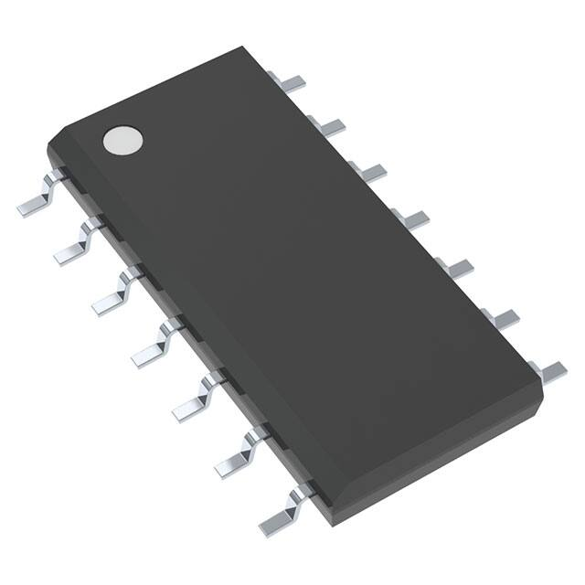
SOIC−14
D SUFFIX
CASE 751AP
GND
WAKE
INH
OTP_ZAP
1
14
2
13
3
12
4
5
6
NCV7420
The NCV7420 is a fully featured local interconnect network (LIN)
transceiver designed to interface between a LIN protocol controller
and the physical bus. The transceiver is implemented in I3T
technology enabling both high−voltage analog circuitry and digital
functionality to co−exist on the same chip.
The NCV7420 LIN device is a member of the in−vehicle
networking (IVN) transceiver family of ON Semiconductor that
integrates a LIN v2.0/2.1 physical transceiver and either a 3.3 V or a
5 V voltage regulator.
The LIN bus is designed to communicate low rate data from control
devices such as door locks, mirrors, car seats, and sunroofs at the
lowest possible cost. The bus is designed to eliminate as much wiring
as possible and is implemented using a single wire in each node. Each
node has a slave MCU−state machine that recognizes and translates
the instructions specific to that function. The main attraction of the
LIN bus is that all the functions are not time critical and usually relate
to passenger comfort.
7
11
10
9
8
VCC
RxD
TxD
GND
STB
EN
TEST
ORDERING INFORMATION
See detailed ordering and shipping information in the package
dimensions section on page 19 of this data sheet.
KEY FEATURES
EMI Compatibility
LIN−Bus Transceiver
• LIN compliant to specification revision 2.0 and 2.1
•
•
•
• Integrated slope control
• Meets most demanding EMS/EME requirements
(backward compatible to version 1.3) and J2602
I3T high voltage technology
Bus voltage ±45 V
Transmission rate up to 20 kBaud
Modes
• Normal mode: LIN communication in either low (up to
10 kBaud) or normal slope
• Sleep mode: VCC is switched “off” and no
Protection
• Thermal shutdown
• Indefinite short−circuit protection on pins LIN and
•
•
•
communication on LIN bus
• Standby mode: VCC is switched “on” but there is no
WAKE towards supply and ground
Load dump protection (45 V)
Bus pins protected against transients in an automotive
environment
System ESD protection level for LIN, WAKE and VBB
up to ±12 kV
•
Quality
Voltage Regulator
•
•
•
•
• NCV Prefix for Automotive and Other Applications
Output voltage 5 V / ~50 mA or 3.3 V / ~50 mA
Wake−up input
Enable inputs for standby and sleep mode
INH output for auxiliary purposes (switching of an
external pull−up or resistive divider towards battery,
control of an external voltage regulator etc.)
© Semiconductor Components Industries, LLC, 2015
May, 2015 − Rev. 9
communication on LIN bus
Wake−up bringing the component from sleep mode into
standby mode is possible either by LIN command or
digital input signal on WAKE pin. Wake−up from LIN
bus can also be detected and flagged when the chip is
already in standby mode.
•
1
Requiring Unique Site and Control Change Require−
ments; AEC−Q100 Qualified and PPAP Capable
These Devices are Pb−Free, Halogen Free/BFR Free
and are RoHS Compliant
Publication Order Number:
NCV7420/D
�NCV7420
MARKING DIAGRAM
14
NCV7420 = Specific Device Code
−x
= −3 = NCV7420D23G
= −4 = NCV7420D24G
= −5 = NCV7420D25G
= −6 = NCV7420D26G
A
= Assembly Location
WL
= Wafer Lot
Y
= Year
WW
= Work Week
G
= Pb−Free Package
NCV7420−x
AWLYWWG
1
Table 1. KEY TECHNICAL CHARACTERISTICS − 3.3 V version
Symbol
VBB
IBB_SLP
Parameter
Nominal battery operating voltage (Note 1)
Min
Typ
Max
Unit
5
12
26
V
Load dump protection (Note 2)
45
Supply current in sleep mode
20
mA
V
VCC_OUT
(Note 4)
Regulated VCC output, VCC load 1 mA−30 mA
3.23
3.30
3.37
Regulated VCC output, VCC load 0 mA−50 mA
3.19
3.30
3.41
IOUT_MAX
Maximum VCC output current (Note 3)
50
Operating DC voltage on WAKE pin
0
VBB
Maximum rating voltage on WAKE pin
−45
45
Junction thermal shutdown temperature
165
195
°C
Operating junction temperature
−40
+150
°C
VWAKE
TJSD
TJ
mA
V
Table 2. KEY TECHNICAL CHARACTERISTICS − 5 V version
Symbol
VBB
IBB_SLP
Parameter
Nominal battery operating voltage (Note 1)
Min
Typ
Max
Unit
6
12
26
V
Load dump protection
45
Supply current in sleep mode
20
mA
V
VCC_OUT
(Note 4)
Regulated VCC output, VCC load 1 mA−30 mA
4.9
5.0
5.1
Regulated VCC output, VCC load 0 mA−50 mA
4.83
5.0
5.17
IOUT_MAX
Maximum VCC output current (Note 3)
VWAKE
TJSD
TJ
50
Operating DC voltage on WAKE pin
mA
V
0
VBB
Maximum rating voltage on WAKE pin
−45
45
Junction thermal shutdown temperature
165
195
°C
Operating junction temperature
−40
+150
°C
1. Below 5 V on VBB in normal mode, the bus will either stay recessive or comply with the voltage level specifications and transition time
specifications as required by SAE J2602. It is ensured by the battery monitoring circuit.
2. The applied transients shall be in accordance with ISO 7637 part 1, test pulse 5. The device complies with functional class C; class A can
be reached depending on the application and external conditions.
3. Thermal aspects of the entire end−application have to be taken into account in order to avoid thermal shutdown of NCV7420.
4. VCC voltage regulator output must be properly decoupled by external capacitor of min. 8 mF with ESR < 1 W to ensure stability.
Table 3. THERMAL CHARACTERISTICS
Symbol
Parameter
Conditions
Value
Unit
RqJA1
Thermal resistance junction−to−ambient, 1S0P PCB (Note 5)
free air
140
K/W
RqJA2
Thermal resistance junction−to−ambient, 2S2P PCB (Note 6)
free air
80
K/W
5. Test board according to EIA/JEDEC Standard JESD51−3, signal layer with 20% trace coverage
6. Test board according to EIA/JEDEC Standard JESD51−7, signal layers with 20% trace coverage
www.onsemi.com
2
�NCV7420
VCC
VBB
INH
NCV7420
Osc
Band−
gap
V−reg
VBB
WAKE
VCC
VBB
POR
VCC
STB
Thermal
shutdown
Control Logic
VBB
EN
VCC
Standby
Sleep
Normal
mode
RxD
LIN
Receiver
VCC
Timeout
TxD
TEST
Driver &
Slope
Control
OTP_ZAP
GND
Figure 1. Block Diagram
Typical Application
determined by the length and capacitance of the LIN bus, the
number and capacitance of Slave devices, the pull−up
resistance of all devices (Master & Slave), and the required
time constant of the system, respectively.
VCC voltage must be properly stabilized by external
capacitor: capacitor of min. 8 mF (ESR < 1 W).
Application Schematic
The EMC immunity of the Master−mode device can be
further enhanced by adding a capacitor between the LIN
output and ground. The optimum value of this capacitor is
www.onsemi.com
3
�NCV7420
Master Node
10uF
VBB
WAKE
10nF
GND
WAKE
OTP_ZAP
TxD
LIN
Micro
controller
EN
WAKE
STB
TEST
GND
GND
GND
LIN
220pF
1 nF
LIN
WAKE
OTP_ZAP
Slave Node
VCC
VCC
RxD
INH
10nF
NCV7420
1kW
LIN
VBB
VCC
VCC
RxD
INH
10uF
10uF 100nF
VBAT
NCV7420
10uF 100nF
VBAT
GND
TxD
Micro
controller
EN
STB
TEST
GND
KL30
LIN−BUS
KL31
Figure 2. Typical Application Diagram
Table 4. PIN DESCRIPTION
Pin
Name
Description
1
VBB
Battery supply input
2
LIN
LIN bus output/input
3
GND
Ground
4
GND
Ground
5
WAKE
6
INH
7
OTP_ZAP
8
TEST
9
EN
Enable input, transceiver in normal operation mode when high
10
STB
Standby mode control input
11
GND
Ground
12
TxD
Transmit data input, low in dominant state
13
RxD
Receive data output; low in dominant state; push−pull output
14
VCC
Supply voltage (output)
High voltage digital input pin to switch the part from sleep− to standby mode
Inhibit output
Supply for programming of trimming bits at factory testing, should be grounded in the application
Digital input for factory testing, should be grounded in the application
Overall Functional Description
with EMC performance due to reduced slew rate of the LIN
output.
The junction temperature is monitored via a thermal
shutdown circuit that switches the LIN transmitter and
voltage regulator off when temperature exceeds the TSD
trigger level.
NCV7420 has four operating states (normal mode, low
slope mode, standby mode, and sleep mode) that are
determined by the input signals EN, WAKE, STB, and TxD.
LIN is a serial communication protocol that efficiently
supports the control of mechatronic nodes in distributed
automotive applications. The domain is class−A multiplex
buses with a single master node and a set of slave nodes.
NCV7420 is designed as a master or slave node for the
LIN communication interface with an integrated 3.3 V or
5 V voltage regulator having a current capability up to
50 mA for supplying any external components
(microcontroller).
NCV7420 contains the LIN transmitter, LIN receiver,
voltage regulator, power−on−reset (POR) circuits and
thermal shutdown (TSD). The LIN transmitter is optimized
for the maximum specified transmission speed of 20 kBaud
Operating States
NCV7420 provides four operating states, two modes for
normal operation with communication, one standby without
communication and one low power mode with very low
current consumption. See Figure 3.
www.onsemi.com
4
�NCV7420
Normal mode
(normal slope)
−VCC: “on”
−LIN TX: “on”
−Term: 30 kW
−INH: “high”/“floating”
−RxD: LIN Data (push−pull)
EN goes from 1 to 0
EN goes from 1 to 0
Note:
LIN Transmitter is “off” when
VBB < VBB_UV_th
EN goes from 1 to 0
while STB = 1 or VBB < VBB_UV_th
while STB = 1 or VBB < VBB_UV_th
EN goes from 0 to 1 while TxD = 0,
−VCC: “on”
−LIN TX: “off”
−Term: “current source”
−INH: “floating”
−RxD: pull−up to VCC/low
and VCC > VCC_UV_th, VBB > VBB_UV_th
from any mode
VBB < PORL_VBB
Power off
and VCC > VCC_UV_th and VBB > VBB_UV_th
Local wake−up
or LIN wake−up
Normal mode
(low slope)
while STB = 0 and VBB > VBB_UV_th
EN goes from 0 to 1 while TxD = 1,
Standby mode
Power up VBB
VBB > VBB_UV_th
Sleep mode
−VCC: “on”
−LIN TX: “on”
−Term: 30 kW
−INH: “high”/“floating”
−RxD: LIN data (push−pull)
EN goes from 1 to 0
while STB = 0 and VBB > VBB_UV_th
−VCC: “off”
−LIN TX: “off”
−Term: “current source”
−INH: “floating”
−RxD: pull−up to VCC
Figure 3. State Diagram
Table 5. MODE SELECTION
Mode
VCC
RxD
INH
LIN
30 kW on LIN
Note
Normal −
Slope
ON
Low = Dominant State
High = Recessive State
High if STB=High during state
transition; Floating otherwise
Normal
Slope
ON
(Note 7)
Normal −
Low Slope
ON
Low = Dominant State
High = Recessive State
High if STB=High during state
transition; Floating otherwise
Low Slope
ON
(Note 8)
Standby
ON
Low after LIN wake−up,
high otherwise
Floating
OFF
OFF
(Notes 9
and 10)
Sleep
OFF
Clamped to VCC
Floating
OFF
OFF
7. The normal slope mode is entered when pin EN goes HIGH while TxD is in HIGH state during EN transition.
8. The low slope mode is entered when pin EN goes HIGH while TxD is in LOW state during EN transition. LIN transmitter gets on only after
TxD returns to high after the state transition.
9. The standby mode is entered automatically after power−up.
10. In standby mode, RxD High state is achieved by internal pull-up resistor to VCC.
Normal Slope Mode
HIGH. If STB pin is high during the standby-to-normal
slope mode transition, INH pin is pulled high. Otherwise, it
stays floating.
In normal slope mode the transceiver can transmit and
receive data via LIN bus with speed up to 20 kBaud. The
transmit data stream of the LIN protocol is present on the
TxD pin and converted by the transmitter into a LIN bus
signal with controlled slew rate to minimize EMC emission.
The receiver consists of the comparator that has a threshold
with hysteresis in respect to the supply voltage and an input
filter to remove bus noise. The LIN output is pulled HIGH
via an internal 30 kW pull-up resistor. For master
applications it is needed to put an external 1 kW resistor with
a serial diode between LIN and VBB (or INH). See Figure 2.
The mode selection is done by EN=HIGH when TxD pin is
Low Slope Mode
In low slope mode the slew rate of the signal on the LIN
bus is reduced (rising and falling edges of the LIN bus signal
are longer). This further reduces the EMC emission. As a
consequence the maximum speed on the LIN bus is reduced
up to 10 kBaud. This mode is suited for applications where
the communication speed is not critical. The mode selection
is done by EN=HIGH when TxD pin is LOW. In order not
to transmit immediately a dominant state on the bus (because
www.onsemi.com
5
�NCV7420
Sleep Mode
TxD=LOW), the LIN transmitter is enabled only after TxD
returns to HIGH. If STB pin is high during the
standby−to−low slope mode transition, INH pin is pulled
high. Otherwise, it stays floating.
The Sleep Mode provides extreme low current
consumption. This mode is entered when both EN and STB
pins are LOW coming from normal mode. The internal
termination resistor of 30 kW between LIN and VBB is
disconnected and also the VCC regulator is switched off to
minimize current consumption.
Standby Mode
The standby mode is always entered after power−up of the
NCV7420. It can also be entered from normal mode when
the EN pin is low and the standby pin is high. From sleep
mode it can be entered after a local wake−up or LIN
wake−up. In standby mode the VCC voltage regulator for
supplying external components (e.g. a microcontroller)
stays active. Also the LIN receiver stays active to be able to
detect a remote wake−up via bus. The LIN transmitter is
disabled and the slave internal termination resistor of 30 kW
between LIN and VBB is disconnected in order to minimize
current consumption. Only a pull−up current source
between VBB and LIN is active.
Detection of Local Wake−Up
Wake
Wake−up
NCV7420 has two possibilities to wake−up from sleep or
standby mode (see Figure 3):
• Local wake−up: enables the transition from sleep mode
to standby mode
• Remote wake−up via LIN: enables the transition from
sleep− to standby mode and can be also detected when
already in standby mode.
A local wake−up is only detected in sleep mode if a
transition from LOW to HIGH or from HIGH to LOW is
seen on the WAKE pin.
Detection of Local Wake−Up
Wake
VBB
VBB
50% VBB typ.
Sleep Mode
Standby Mode
50% VBB typ.
t
Sleep Mode
t
Standby Mode
Figure 4. Local Wake−up Signal
A remote wake−up is only detected if a combination of (1)
a falling edge at the LIN pin (transition from recessive to
dominant) is followed by (2) a dominant level maintained
for a time period > tWAKE and (3) again a rising edge at pin
LIN (transition from dominant to recessive) happens.
LIN
Detection of Remote Wake−Up
VBB
LIN recessive level
tWAKE
60% VBB
40% VBB
LIN dominant level
Sleep Mode
Standby Mode
t
Figure 5. Remote Wake−up Behavior
• RxD is kept LOW until normal mode is entered after a
The wake−up source is distinguished by pin RxD in the
standby mode:
• RxD remains HIGH after power−up or local wake−up.
remote wake−up (LIN).
www.onsemi.com
6
�NCV7420
VBB_UV_th
PORL_VBB
VBB
VCC
Power off
Standby
Normal
normal slope
Normal
low slope
Standby
Sleep
EN
STB
TxD
Wake−up (Local or LIN)
Figure 6. Operating Modes Transitions
www.onsemi.com
7
Standby
Power off
�NCV7420
Electrical Characteristics
Definitions
All voltages are referenced to GND (Pin 11). Positive currents flow into the IC.
Table 6. ABSOLUTE MAXIMUM RATINGS – 3.3 V and 5 V versions
Symbol
Parameter
VBB
Battery voltage on pin VBB (Note 11)
Min
Max
Unit
−0.3
+45
V
+7
VCC
DC voltage on pin VCC
0
IVCC
Current delivered by the VCC regulator
50
VLIN
LIN bus voltage (Note 12)
−45
+45
V
VINH
DC voltage on inhibit pin
−0.3
VBB + 0.3
V
VWAKE
DC voltage on WAKE pin
−45
45
V
VDIG_IN
DC input voltage on pins TxD, RxD, EN, STB
−0.3
VCC + 0.3
V
Maximum junction temperature
−40
+165
°C
Electrostatic discharge voltage on all pins; HBM (Note 13)
−2
+2
kV
Electrostatic discharge voltage on LIN, INH, WAKE and VBB towards GND; HBM (Note 13)
−4
+4
kV
Electrostatic discharge on LIN, WAKE and VBB; system HBM (Note 14)
−8
+8
kV
Electrostatic discharge voltage on all pins; CDM (Note 16)
−500
+500
V
Electrostatic discharge voltage on all pins; HBM (Note 13)
−4
+4
kV
TJ
VESD
VESD
(EMC/ESD
improved
versions)
V
mA
Electrostatic discharge voltage on LIN, INH, WAKE and VBB towards GND; HBM (Note 13)
−6
+6
kV
Electrostatic discharge on LIN, WAKE and VBB; system HBM (Note 15)
−12
+12
kV
Electrostatic discharge voltage on all pins; CDM (Note 16)
−750
+750
V
Stresses exceeding those listed in the Maximum Ratings table may damage the device. If any of these limits are exceeded, device functionality
should not be assumed, damage may occur and reliability may be affected.
11. The applied transients shall be in accordance with ISO 7637 part 1, test pulses 1, 2, 3a, 3b, and 5. The device complies with functional class
C; class A can be reached depending on the application and external components.
12. The applied transients shall be in accordance with ISO 7637 part 1, test pulses 1, 2, 3a, and 3b. The device complies with functional class
C; class A can be reached depending on the application and external components.
13. Equivalent to discharging a 100 pF capacitor through a 1500 W resistor.
14. Equivalent to discharging a 150 pF capacitor through a 330 W resistor conform to IEC Standard 61000−4−2. LIN bus filter 220 pF, VBB blocking
capacitor 100 nF, 3k3/10n R/C network on WAKE.
15. Equivalent to discharging a 150 pF capacitor through a 330 W resistor conform to IEC Standard 61000−4−2. No filter on LIN, VBB blocking
capacitor 100 nF, 3k3/10n R/C network on WAKE.
16. Charged device model according ESD-STM5.3.1.
www.onsemi.com
8
�NCV7420
Table 7. DC CHARACTERISTICS – 3.3 V version
(VBB = 5 V to 26 V; TJ = −40°C to +150°C; Bus Load = 500 W (VBB to LIN); unless otherwise specified.)
Symbol
Parameter
Conditions
Min
Typ
Max
Unit
SUPPLY − Pin VBB
IBB_ON
Supply current
Normal mode; LIN recessive
1.6
mA
IBB_STB
Supply current
Standby mode, VBB =
5–18 V, TJ < 105°C
70
mA
IBB_SLP
Supply current
Sleep mode, VBB = 5–18 V,
TJ < 105°C
20
mA
V
VOLTAGE REGULATOR − Pin VCC
VCC_OUT
IOUT_MAX_ABS
IOUT_LIM
DVCC_OUT
VDO
Regulator output voltage
Absolute maximum output current
VCC load 1 mA − 30 mA
3.23
3.30
3.37
VCC load 0 mA − 50 mA
3.19
3.30
3.41
Thermal shutdown must be
taken into account
Overcurrent limitation
50
100
50
mA
170
mA
Line Regulation (Note 22)
VBB 5−26 V, IOUT = 5 mA,
TJ = 25°C
0.5
mV
Load Regulation (Note 22)
IOUT 1−50 mA, VBB = 14 V,
TJ = 25°C
45
mV
IOUT = 1 mA, TJ = 25°C
13
mV
IOUT = 10 mA, TJ = 25°C
134
mV
IOUT = 50 mA, TJ = 25°C
732
mV
Dropout Voltage (VBB−VCC_OUT)
Figure 11, (Notes 21, 22)
LIN TRANSMITTER − Pin LIN
VLIN_dom_LoSup
LIN dominant output voltage
TxD = low; VBB = 7.3 V
1.2
V
VLIN_dom_HiSup
LIN dominant output voltage
TxD = low; VBB = 18 V
2.0
V
VLIN_REC
LIN Recessive Output Voltage (Note 17)
ILIN_lim
Short circuit current limitation
RSLAVE
Internal pull−up resistance
CLIN
TxD = high; ILIN = 10 mA
VBB − 1.5
VBB
V
VLIN = VBB_MAX
40
200
mA
33
47
kW
15
25
pF
0.4
VBB
20
Capacitance on pin LIN (Note 19)
LIN RECEIVER − Pin LIN
Vbus_dom
Bus voltage for dominant state
Vbus_rec
Bus voltage for recessive state
Vrec_dom
Receiver threshold
LIN bus recessive → dominant
Vrec_rec
Receiver threshold
LIN bus dominant → recessive
Vrec_cnt
Receiver centre voltage
(Vrec_dom + Vrec_rec) / 2
Vrec_hys
Receiver hysteresis
(Vrec_rec − Vrec_dom)
0.05
ILIN_off_dom
LIN output current bus in dominant state
Driver off; VBB = 12 V,
VLIN = 0 V
−1
ILIN_off_rec
LIN output current bus in recessive state
Driver off; VBB < 18 V
VBB < VLIN < 18 V
ILIN_no_GND
0.6
Communication not affected
VBB = GND = 12 V;
0 < VLIN < 18 V
0.4
VBB
0.6
VBB
0.4
0.6
VBB
0.475
0.525
VBB
0.175
VBB
−1
mA
1
mA
1
mA
17. The voltage drop in Normal mode between LIN and VBB pin is the sum of the diode drop and the drop at serial pull−up resistor. The drop
at the switch is negligible. See Figure 1.
18. By one of the trimming bits, following reconfiguration can be done during chip−level testing in order to fit the NCV7420−3 into different
interface: pins TxD and EN will have typ. 10 kW pull−down resistor to ground and pin WAKE will have typ. 10 mA pull−up current source.
19. Guaranteed by design. Not tested.
20. VBB undervoltage threshold is always higher than VBB POR low level (VBB_UV_th > PORL_VBB)
21. Measured at output voltage VCC_OUT = (VCC_OUT@VBB = 5 V) – 2%.
22. Values based on design and characterization. Not tested in production.
www.onsemi.com
9
�NCV7420
Table 7. DC CHARACTERISTICS – 3.3 V version
(VBB = 5 V to 26 V; TJ = −40°C to +150°C; Bus Load = 500 W (VBB to LIN); unless otherwise specified.)
Symbol
Parameter
Conditions
Min
Typ
Max
Unit
5
mA
0.65
VBB
1
mA
54
ms
0.8
V
LIN RECEIVER − Pin LIN
ILIN_no_VBB
LIN bus remains operational
VBB = GND = 0 V;
0 < VLIN < 18 V
Pin WAKE
VWAKE_th
ILEAK
tWAKE_MIN
Threshold voltage
0.35
Input leakage current (Note 18)
VWAKE = 0 V; VBB = 18 V
−1
Sleep mode; rising
and falling edge
8
Debounce time
−0.5
Pins TxD and STB
VIL
Low level input voltage
VIH
High level input voltage
2.0
RPU
Pull−up resistance to VCC (Note 18)
50
V
200
kW
Pin INH
Delta_VH
ILEAK
High level voltage drop
IINH = 15 mA
Leakage current
Sleep mode; VINH = 0 V
0.35
−1
0.75
V
1
mA
0.8
V
Pin EN
VIL
Low level input voltage
VIH
High level input voltage
2.0
RPD
Pull−down resistance to ground (Note 18)
50
V
200
kW
0.65
V
Pin RxD
VOL
Low level output voltage
ISINK = 2 mA
VOH
High level output voltage
(In Normal mode)
Normal mode,
ISOURCE = −2 mA
VCC −
0.65 V
RPU
Pull−up resistance to VCC
(In Standby and Sleep mode)
Standby mode,
Sleep mode
5
10
15
kW
3
4.2
4.75
V
NCV7420D23
2.5
4.2
V
NCV7420D24
1.7
3.8
V
2
3
V
165
195
°C
9
18
°C
V
POR AND VOLTAGE MONITOR
VBB_UV_th
VBB undervoltage threshold (Note 20)
PORL_VBB
VBB POR low level comparator
VCC_UV_th
VCC undervoltage threshold
THERMAL SHUTDOWN
TJSD
TJSD_HYST
Thermal Shutdown Junction Temperature
For shutdown
Thermal shutdown hysteresis
17. The voltage drop in Normal mode between LIN and VBB pin is the sum of the diode drop and the drop at serial pull−up resistor. The drop
at the switch is negligible. See Figure 1.
18. By one of the trimming bits, following reconfiguration can be done during chip−level testing in order to fit the NCV7420−3 into different
interface: pins TxD and EN will have typ. 10 kW pull−down resistor to ground and pin WAKE will have typ. 10 mA pull−up current source.
19. Guaranteed by design. Not tested.
20. VBB undervoltage threshold is always higher than VBB POR low level (VBB_UV_th > PORL_VBB)
21. Measured at output voltage VCC_OUT = (VCC_OUT@VBB = 5 V) – 2%.
22. Values based on design and characterization. Not tested in production.
www.onsemi.com
10
�NCV7420
Table 8. DC CHARACTERISTICS – 5 V version
(VBB = 6 V to 26 V; TJ = −40°C to +150°C; Bus Load = 500 W (VBB to LIN); unless otherwise specified.)
Symbol
Parameter
Conditions
Min
Typ
Max
Unit
SUPPLY − Pin VBB
IBB_ON
Supply current
Normal mode; LIN recessive
1.6
mA
IBB_STB
Supply current
Standby mode,
VBB = 6–18 V,
TJ < 105°C
70
mA
IBB_SLP
Supply current
Sleep mode, VBB = 6–18 V,
TJ < 105°C
20
mA
V
VOLTAGE REGULATOR − Pin VCC
VCC_OUT
IOUT_MAX_ABS
IOUT_LIM
DVCC_OUT
VDO
Regulator output voltage
Absolute maximum output current
VCC load 1 mA − 30 mA
4.9
5.0
5.1
VCC load 0 mA − 50 mA
4.83
5.0
5.17
Thermal shutdown must be
taken into account
Overcurrent limitation
50
100
50
mA
170
mA
Line Regulation (Note 28)
VBB 6−26 V, IOUT = 5 mA,
TJ = 25°C
0.9
mV
Load Regulation (Note 28)
IOUT 1−50 mA, VBB = 14 V,
TJ = 25°C
74
mV
IOUT = 1 mA, TJ = 25°C
13
mV
IOUT = 10 mA, TJ = 25°C
136
mV
IOUT = 50 mA, TJ = 25°C
794
mV
Dropout Voltage (VBB−VCC_OUT)
Figure 19 (Notes 27, 28)
LIN TRANSMITTER − Pin LIN
VLIN_dom_LoSup
LIN dominant output voltage
TxD = low; VBB = 7.3 V
1.2
V
VLIN_dom_HiSup
LIN dominant output voltage
TxD = low; VBB = 18 V
2.0
V
VLIN_rec
LIN Recessive Output Voltage (Note 23)
ILIN_lim
Short circuit current limitation
RSLAVE
Internal pull−up resistance
CLIN
TxD = high; ILIN = 10 mA
VBB − 1.5
VBB
V
VLIN = VBB_MAX
40
200
mA
33
47
kW
15
25
pF
Typ
Max
Unit
0.4
VBB
20
Capacitance on pin LIN (Note 25)
LIN RECEIVER − Pin LIN
Symbol
Parameter
Conditions
Min
Vbus_dom
Bus voltage for dominant state
Vbus_rec
Bus voltage for recessive state
Vrec_dom
Receiver threshold
LIN bus recessive → dominant
Vrec_rec
Receiver threshold
LIN bus dominant → recessive
Vrec_cnt
Receiver center voltage
(Vrec_dom + Vrec_rec) / 2
Vrec_hys
Receiver hysteresis
(Vrec_rec − Vrec_dom)
0.05
ILIN_off_dom
LIN output current bus in dominant state
Driver off; VBB = 12 V;
VLIN = 0 V
−1
ILIN_off_rec
LIN output current bus in recessive state
Driver off; VBB < 18 V
VBB < VLIN < 18 V
0.6
0.4
VBB
0.6
VBB
0.4
0.6
VBB
0.475
0.525
VBB
0.175
VBB
mA
1
mA
23. The voltage drop in Normal mode between LIN and VBB pin is the sum of the diode drop and the drop at serial pull−up resistor. The drop
at the switch is negligible. See Figure 1.
24. By one of the trimming bits, following reconfiguration can be done during chip−level testing in order to fit the NCV7420−5 into different
interface: pins TxD and EN will have typ. 10 kW pull−down resistor to ground and pin WAKE will have typ. 10 mA pull−up current source.
25. Guaranteed by design. Not tested.
26. VBB undervoltage threshold is always higher than VBB POR low level (VBB_UV_th > PORL_VBB)
27. Measured at output voltage VCC_OUT = (VCC_OUT@VBB = 6 V) – 2%.
28. Values based on design and characterization. Not tested in production.
www.onsemi.com
11
�NCV7420
Table 8. DC CHARACTERISTICS – 5 V version
(VBB = 6 V to 26 V; TJ = −40°C to +150°C; Bus Load = 500 W (VBB to LIN); unless otherwise specified.)
Symbol
Parameter
Conditions
Min
−1
Typ
Max
Unit
1
mA
5
mA
0.65
VBB
LIN RECEIVER − Pin LIN
ILIN_no_GND
Communication not affected
VBB = GND = 12 V;
0 < VLIN < 18 V
ILIN_no_VBB
LIN bus remains operational
VBB = GND = 0 V;
0 < VLIN < 18 V
Pin WAKE
VWAKE_th
ILEAK
tWAKE_MIN
Threshold voltage
0.35
Input leakage current (Note 24)
VWAKE = 0 V; VBB = 18 V
−1
Sleep mode; rising and
falling edge
8
Debounce time
−0.5
1
mA
54
ms
0.8
V
Pins TxD and STB
VIL
Low level input voltage
VIH
High level input voltage
2.0
RPU
Pull−up resistance to VCC (Note 24)
50
V
200
kW
0.75
V
1
mA
0.8
V
Pin INH
Delta_VH
ILEAK
High level voltage drop
IINH = 15 mA
Leakage current
Sleep mode; VINH = 0 V
0.35
−1
Pin EN
VIL
Low level input voltage
VIH
High level input voltage
2.0
RPD
Pull−down resistance to ground (Note 24)
50
V
200
kW
0.65
V
Pin RxD
VOL
Low level output voltage
ISINK = 2 mA
VOH
High level output voltage
(In Normal mode)
Normal mode,
ISOURCE = −2 mA
VCC −
0.65 V
RPU
Pull−up resistance to VCC
(In Standby and Sleep mode)
Standby mode,
Sleep mode
5
10
15
kW
3
4.2
4.75
V
V
POR AND VOLTAGE MONITOR
VBB_UV_th
VBB undervoltage threshold (Note 26)
PORL_VBB
VBB POR low level comparator
VCC_UV_th
NCV7420D25
2.5
4.2
V
NCV7420D26
1.7
3.8
V
3
4.5
V
165
195
°C
9
18
°C
VCC undervoltage threshold
THERMAL SHUTDOWN
TJSD
TJSD_HYST
Thermal Shutdown Junction Temperature
For shutdown
Thermal shutdown hysteresis
23. The voltage drop in Normal mode between LIN and VBB pin is the sum of the diode drop and the drop at serial pull−up resistor. The drop
at the switch is negligible. See Figure 1.
24. By one of the trimming bits, following reconfiguration can be done during chip−level testing in order to fit the NCV7420−5 into different
interface: pins TxD and EN will have typ. 10 kW pull−down resistor to ground and pin WAKE will have typ. 10 mA pull−up current source.
25. Guaranteed by design. Not tested.
26. VBB undervoltage threshold is always higher than VBB POR low level (VBB_UV_th > PORL_VBB)
27. Measured at output voltage VCC_OUT = (VCC_OUT@VBB = 6 V) – 2%.
28. Values based on design and characterization. Not tested in production.
www.onsemi.com
12
�NCV7420
AC Characteristics – 3.3 V and 5 V versions − (VBB = 7 V to 18 V; TJ = −40°C to +150°C; unless otherwise specified.)
Table 9. AC CHARACTERISTICS LIN TRANSMITTER − Pin LIN
Symbol
Conditions
Min
D1
Duty Cycle 1 = tBUS_REC(min) / (2 x tBIT)
see Figure 23
Parameter
Normal slope mode
THREC(max) = 0.744 x VBB
THDOM(max) = 0.581 x VBB
tBIT = 50 ms
VBB = 7 V to 18 V
0.396
Typ
Max
0.5
D2
Duty Cycle 2 = tBUS_REC(max) / (2 x tBIT)
see Figure 23
Normal slope mode
THREC(min) = 0.422 x VBB
THDOM(min) = 0.284 x VBB
tBIT = 50 ms
VBB = 7.6 V to 18 V
0.5
0.581
D3
Duty Cycle 3 = tBUS_REC(min) / (2 x tBIT)
see Figure 23
Normal slope mode
THREC(max) = 0.778 x VBB
THDOM(max) = 0.616 x VBB
tBIT = 96 ms
VBB = 7 V to 18 V
0.417
0.5
D4
Duty Cycle 4 = tBUS_REC(max) / (2 x tBIT)
see Figure 23
Normal slope mode
THREC(min) = 0.389 x VBB
THDOM(min) = 0.251 x VBB
tBIT = 96 ms
VBB = 7.6 V to 18 V
0.5
0.590
Unit
ttrx_prop_down
Propagation Delay of TxD to LIN. TxD
high to low
(Note 29)
6
ms
ttrx_prop_up
Propagation Delay of TxD to LIN. TxD
low to high
(Note 29)
6
ms
tfall_norm
LIN falling edge
Normal slope mode;
VBB = 12 V; L1, L2
(Note 30)
22.5
ms
trise_norm
LIN rising edge
Normal slope mode;
VBB = 12 V; L1, L2
(Note 30)
22.5
ms
tsym_norm
LIN slope symmetry
Normal slope mode;
VBB = 12 V; L1, L2
(Note 30)
4
ms
tfall_norm
LIN falling edge
Normal slope mode;
VBB = 12 V; L3 (Note 30)
27
ms
trise_norm
LIN rising edge
Normal slope mode;
VBB = 12 V; L3 (Note 30)
27
ms
tsym_norm
LIN slope symmetry
Normal slope mode;
VBB = 12 V; L3 (Note 30)
5
ms
−4
−5
tfall_low
LIN falling edge
Low slope mode (Note 31);
VBB = 12 V; L3 (Note 30)
62
ms
trise_low
LIN rising edge
Low slope mode (Note 31);
VBB = 12 V; L3 (Note 30)
62
ms
30
150
ms
6
20
ms
twake
Dominant timeout for wake−up via LIN bus
tdom
TxD dominant timeout
TxD = low
29. Values based on design and characterization. Not tested in production.
30. The AC parameters are specified for following RC loads on the LIN bus: L1 = 1 kW / 1 nF; L2 = 660 W / 6.8 nF; L3 = 500 W / 10 nF.
31. Low slope mode is not compliant to the LIN standard.
www.onsemi.com
13
�NCV7420
REGULATOR TYPICAL PERFORMANCE CHARACTERISTICS − 3.3 V VERSION
Load Transient Responses
VBB = 14 V
CVBB = 10 mF + 100 nF
CVCC = 10 mF X7R
DVCC
(20 mV/DIV)
LOAD CURRENT (mA)
LOAD CURRENT (mA)
DVCC
(20 mV/DIV)
VBB = 14 V
CVBB = 10 mF + 100 nF
CVCC = 10 mF X7R
50
trise, tfall = 10 ms
0.1
50
trise, tfall = 10 ms
1
TIME (500 ms/DIV)
TIME (500 ms/DIV)
Figure 7. Load Transient Response
(ICC 100 mA to 50 mA)
Figure 8. Load Transient Response
(ICC 1 mA to 50 mA)
30
20
ICC = 5 mA
CVCC = 10 mF
DVCC
(50 mV/DIV)
ICC = 100 mA
CVCC = 10 mF
INPUT VOLTAGE (V)
INPUT VOLTAGE (V)
DVCC
(20 mV/DIV)
Line Transient Responses
trise, tfall = 10 ms
10
0
30
20
trise, tfall = 10 ms
10
0
TIME (2 ms/DIV)
TIME (1 ms/DIV)
Figure 9. Line Transient Response
(VBB 5 V to 26 V)
Figure 10. Line Transient Response
(VBB 5 V to 26 V)
www.onsemi.com
14
�NCV7420
REGULATOR TYPICAL PERFORMANCE CHARACTERISTICS − 3.3 V VERSION
Static Characteristics
3.32
1.4
CVCC = 10 mF X7R
VCC OUTPUT VOLTAGE (V)
DROPOUT VOLTAGE (V)
1.2
50 mA
1.0
0.8
0.6
25 mA
(PORL_VBB
reached at low
temperatures)
0.4
10 mA
0.2
3.30
3.29
−40°C
3.28
25°C
3.27
3.26
85°C
135°C
3.25
0
−50
150°C
3.24
−25
0
25
50
75
100
125
0
150
5
10
15
20
25
30
35
40
45
50
TEMPERATURE (°C)
ICC OUTPUT CURRENT (mA)
Figure 11. Dropout Voltage vs. Temperature
Figure 12. Output Voltage vs. Output Current
3.32
200
160
140
VCC OUTPUT VOLTAGE (V)
VBB = 14 V
CVBB = 10 mF + 100 nF
CVCC = 10 mF X7R
Standby Mode
T = 25°C
180
IBB−ICC (mA)
VBB = 14 V
CVBB = 10 mF + 100 nF
CVCC = 10 mF X7R
3.31
120
100
80
60
40
0
0
5
10
15
20
25
30
35
40
45
3.29
25 mA
3.28
3.27
3.26
3.24
−50
50
10 mA
3.30
3.25
20
1 mA
3.31
50 mA
VBB = 14 V
CVBB = 10 mF + 100 nF
CVCC = 10 mF X7R
−25
0
25
50
75
100
125
ICC OUTPUT CURRENT (mA)
TEMPERATURE (°C)
Figure 13. Ground Current vs. Output Current
Figure 14. Output Voltage vs. Temperature
www.onsemi.com
15
150
�NCV7420
REGULATOR TYPICAL PERFORMANCE CHARACTERISTICS − 5 V VERSION
Load Transient Responses
VBB = 14 V
CVBB = 10 mF + 100 nF
CVCC = 10 mF X7R
DVCC
(50 mV/DIV)
LOAD CURRENT (mA)
LOAD CURRENT (mA)
DVCC
(50 mV/DIV)
VBB = 14 V
CVBB = 10 mF + 100 nF
CVCC = 10 mF X7R
50
trise, tfall = 10 ms
0.1
50
trise, tfall = 10 ms
1
TIME (500 ms/DIV)
TIME (500 ms/DIV)
Figure 15. Load Transient Response
(ICC 100 mA to 50 mA)
Figure 16. Load Transient Response
(ICC 1 mA to 50 mA)
Line Transient Responses
30
20
ICC = 5 mA
CVCC = 10 mF
DVCC
(50 mV/DIV)
INPUT VOLTAGE (V)
INPUT VOLTAGE (V)
DVCC
(20 mV/DIV)
ICC = 100 mA
CVCC = 10 mF
trise, tfall = 10 ms
10
0
30
20
trise, tfall = 10 ms
10
0
TIME (2 ms/DIV)
TIME (1 ms/DIV)
Figure 17. Line Transient Response
(VBB 6 V to 26 V)
Figure 18. Line Transient Response
(VBB 6 V to 26 V)
www.onsemi.com
16
�NCV7420
REGULATOR TYPICAL PERFORMANCE CHARACTERISTICS − 5 V VERSION
Static Characteristics
1.4
5.03
CVCC = 10 mF X7R
50 mA
VCC OUTPUT VOLTAGE (V)
DROPOUT VOLTAGE (V)
1.0
0.8
0.6
25 mA
0.4
10 mA
0.2
0
−50
5.01
5.00 −40°C
4.99
4.98
4.97
4.96
25°C
85°C
4.95
135°C
4.94
4.93
−25
0
25
50
75
100
125
0
150
5
10
15
20
25
30
150°C
35
40
Figure 19. Dropout Voltage vs. Temperature
Figure 20. Output Voltage vs. Output Current
5.03
1 mA
5.02
VCC OUTPUT VOLTAGE (V)
140
120
100
80
60
40
20
5.01
10 mA
5.00
4.99
25 mA
4.98
VBB = 14 V
CVBB = 10 mF + 100 nF
CVCC = 10 mF X7R
4.97
4.96
4.95
4.94
0
0
50
ICC OUTPUT CURRENT (mA)
VBB = 14 V
CVBB = 10 mF + 100 nF
CVCC = 10 mF X7R
Standby Mode
T = 25°C
160
45
TEMPERATURE (°C)
200
180
IBB−ICC (mA)
VBB = 14 V
CVBB = 10 mF + 100 nF
CVCC = 10 mF X7R
5.02
1.2
5
10
15
20
25
30
35
40
45
4.93
−50
50
50 mA
−25
0
25
50
75
100
125
ICC OUTPUT CURRENT (mA)
TEMPERATURE (°C)
Figure 21. Ground Current vs. Output Current
Figure 22. Output Voltage vs. Temperature
www.onsemi.com
17
150
�NCV7420
TxD
tBIT
tBIT
50%
t
tBUS_dom(max)
LIN
tBUS_rec(min)
THRec(max)
THDom(max)
Thresholds of
receiving node 1
THRec(min)
THDom(min)
Thresholds of
receiving node 2
t
tBUS_dom(min)
tBUS_rec(max)
Figure 23. LIN Transmitter Duty Cycle
t BIT
TxD
t BIT
50%
t
LIN
VBB
60% VBB
40% VBB
t
ttrx_prop_down
ttrx_prop_up
Figure 24. LIN Transmitter Timing
LIN
100%
60%
60%
40%
40%
0%
tfall
trise
Figure 25. LIN Transmitter Rising and Falling Times
www.onsemi.com
18
t
�NCV7420
Table 10. AC CHARACTERISTICS LIN RECEIVER
Symbol
Pin LIN
Parameter
Conditions
Min
Typ
Max
Unit
trec_prop_down
Propagation delay of receiver falling edge
0.1
6
ms
trec_prop_up
Propagation delay of receiver rising edge
0.1
6
ms
−2
2
ms
trec_sym
Propagation delay symmetry
trec_prop_down −
trec_prop_up
LIN
VBB
60% VBB
40% VBB
t
RxD
trec_prop_down
trec_prop_up
50%
t
Figure 26. LIN Receiver Timing
ORDERING INFORMATION
Part Number
Temperature
Range
Description
Package
Shipping†
NCV7420D23G
LIN Transceiver + 3.3 V Vreg.
55 / Tube/Rail
NCV7420D23R2G
LIN Transceiver + 3.3 V Vreg.
3000 / Tape & Reel
NCV7420D24G
EMC/ESD Improved LIN
Transceiver + 3.3 V Vreg.
NCV7420D24R2G
EMC/ESD Improved LIN
Transceiver + 3.3 V Vreg.
55 / Tube/Rail
3000 / Tape & Reel
−40°C to 125°C
SOIC−14
(Pb−Free)
NCV7420D25G
LIN Transceiver + 5 V Vreg.
55 / Tube/Rail
NCV7420D25R2G
LIN Transceiver + 5 V Vreg.
NCV7420D26G
EMC/ESD Improved LIN
Transceiver + 5 V Vreg.
55 / Tube/Rail
NCV7420D26R2G
EMC/ESD Improved LIN
Transceiver + 5 V Vreg.
3000 / Tape & Reel
3000 / Tape & Reel
†For information on tape and reel specifications, including part orientation and tape sizes, please refer to our Tape and Reel Packaging
Specifications Brochure, BRD8011/D.
www.onsemi.com
19
�MECHANICAL CASE OUTLINE
PACKAGE DIMENSIONS
SOIC−14
CASE 751AP
ISSUE B
14
1
SCALE 1:1
NOTES 4&5
D
D
0.10 C D
45 5 CHAMFER
NOTES:
1. DIMENSIONING AND TOLERANCING PER ASME Y14.5M, 1994.
2. CONTROLLING DIMENSION: MILLIMETERS.
3. DIMENSION b DOES NOT INCLUDE DAMBAR PROTRUSION.
H
ALLOWABLE PROTRUSION SHALL BE 0.004 mm IN EXCESS OF
MAXIMUM MATERIAL CONDITION.
4. DIMENSION D DOES NOT INCLUDE MOLD FLASH, PROTRUSIONS
OR GATE BURRS. MOLD FLASH, PROTRUSIONS OR GATE BURRS
SHALL NOT EXCEED 0.006 mm PER SIDE. DIMENSION E1 DOES
NOT INCLUDE INTERLEAD FLASH OR PROTRUSION. INTERLEAD
FLASH OR PROTRUSION SHALL NOT EXCEED 0.010 mm PER SIDE.
5. THE PACKAGE TOP MAY BE SMALLER THAN THE PACKAGE BOT
TOM. DIMENSIONS D AND E1 ARE DETERMINED AT THE OUTER
SEATING
L
MOST EXTREMES OF THE PLASTIC BODY AT DATUM H.
C PLANE
6. DIMENSIONS A AND B ARE TO BE DETERMINED AT DATUM H.
DETAIL A
7. DIMENSIONS b AND c APPLY TO THE FLAT SECTION OF THE LEAD
BETWEEN 0.10 TO 0.25 FROM THE LEAD TIP.
8. A1 IS DEFINED AS THE VERTICAL DISTANCE FROM THE SEATING
PLANE TO THE LOWEST POINT ON THE PACKAGE BODY.
h
NOTE 6
A
14
2X
8
0.10 C D
E
E1
NOTES 4&5
L2
0.20 C D
2X
1
7
B
NOTE 6
14X b
0.25
TOP VIEW
M
C A-B D
NOTES 3&7
NOTE 7
c
0.10 C
e
A1
C
SIDE VIEW
NOTE 8
DIM
A
A1
A2
b
c
D
E
E1
e
h
L
L2
DETAIL A
A2
A
DATE 18 MAY 2015
END VIEW
SEATING
PLANE
RECOMMENDED
SOLDERING FOOTPRINT*
MILLIMETERS
MIN
MAX
--1.75
0.10
0.25
1.25
--0.31
0.51
0.10
0.25
8.65 BSC
6.00 BSC
3.90 BSC
1.27 BSC
0.25
0.41
0.40
1.27
0.25 BSC
GENERIC
MARKING DIAGRAM*
14X
0.76
14
XXXXXXXXXG
AWLYWW
14X
1.52
1
7.00
1
1.27
PITCH
DIMENSIONS: MILLIMETERS
*For additional information on our Pb−Free strategy and soldering
details, please download the ON Semiconductor Soldering and
Mounting Techniques Reference Manual, SOLDERRM/D.
DOCUMENT NUMBER:
DESCRIPTION:
98AON30871E
SOIC−14
XXXXX
A
WL
Y
WW
G
= Specific Device Code
= Assembly Location
= Wafer Lot
= Year
= Work Week
= Pb−Free Package
*This information is generic. Please refer to
device data sheet for actual part marking.
Pb−Free indicator, “G” or microdot “ G”,
may or may not be present.
Electronic versions are uncontrolled except when accessed directly from the Document Repository.
Printed versions are uncontrolled except when stamped “CONTROLLED COPY” in red.
PAGE 1 OF 1
ON Semiconductor and
are trademarks of Semiconductor Components Industries, LLC dba ON Semiconductor or its subsidiaries in the United States and/or other countries.
ON Semiconductor reserves the right to make changes without further notice to any products herein. ON Semiconductor makes no warranty, representation or guarantee regarding
the suitability of its products for any particular purpose, nor does ON Semiconductor assume any liability arising out of the application or use of any product or circuit, and specifically
disclaims any and all liability, including without limitation special, consequential or incidental damages. ON Semiconductor does not convey any license under its patent rights nor the
rights of others.
© Semiconductor Components Industries, LLC, 2019
www.onsemi.com
�onsemi,
, and other names, marks, and brands are registered and/or common law trademarks of Semiconductor Components Industries, LLC dba “onsemi” or its affiliates
and/or subsidiaries in the United States and/or other countries. onsemi owns the rights to a number of patents, trademarks, copyrights, trade secrets, and other intellectual property.
A listing of onsemi’s product/patent coverage may be accessed at www.onsemi.com/site/pdf/Patent−Marking.pdf. onsemi reserves the right to make changes at any time to any
products or information herein, without notice. The information herein is provided “as−is” and onsemi makes no warranty, representation or guarantee regarding the accuracy of the
information, product features, availability, functionality, or suitability of its products for any particular purpose, nor does onsemi assume any liability arising out of the application or use
of any product or circuit, and specifically disclaims any and all liability, including without limitation special, consequential or incidental damages. Buyer is responsible for its products
and applications using onsemi products, including compliance with all laws, regulations and safety requirements or standards, regardless of any support or applications information
provided by onsemi. “Typical” parameters which may be provided in onsemi data sheets and/or specifications can and do vary in different applications and actual performance may
vary over time. All operating parameters, including “Typicals” must be validated for each customer application by customer’s technical experts. onsemi does not convey any license
under any of its intellectual property rights nor the rights of others. onsemi products are not designed, intended, or authorized for use as a critical component in life support systems
or any FDA Class 3 medical devices or medical devices with a same or similar classification in a foreign jurisdiction or any devices intended for implantation in the human body. Should
Buyer purchase or use onsemi products for any such unintended or unauthorized application, Buyer shall indemnify and hold onsemi and its officers, employees, subsidiaries, affiliates,
and distributors harmless against all claims, costs, damages, and expenses, and reasonable attorney fees arising out of, directly or indirectly, any claim of personal injury or death
associated with such unintended or unauthorized use, even if such claim alleges that onsemi was negligent regarding the design or manufacture of the part. onsemi is an Equal
Opportunity/Affirmative Action Employer. This literature is subject to all applicable copyright laws and is not for resale in any manner.
PUBLICATION ORDERING INFORMATION
LITERATURE FULFILLMENT:
Email Requests to: orderlit@onsemi.com
onsemi Website: www.onsemi.com
◊
TECHNICAL SUPPORT
North American Technical Support:
Voice Mail: 1 800−282−9855 Toll Free USA/Canada
Phone: 011 421 33 790 2910
Europe, Middle East and Africa Technical Support:
Phone: 00421 33 790 2910
For additional information, please contact your local Sales Representative
�


 工商网监
湘ICP备2023018690号
工商网监
湘ICP备2023018690号
